

Page 1

Motor driver ICs
3-phase motor driver and reversible
motor driver
BA6872AFM
The BA6872AFM has a 3-phase motor driver for VCR capstans, and a reversible motor driver for VCR loading. The capstan motor driver uses the three-phase, pseudo-linear drive method, and has a built-in torque ripple cancellation circuit,
and an output transistor saturation prevention circuit. The loading motor driver has two logic inputs which are used to
set the four operation modes (forward, reverse, stopped (idle) and brake.
Applications
VCR capstan motors, VCR loading motors
Features
1) 3-phase, pseudo-linear drive system.
2) Torque ripple cancellation circuit.
3) Output transistor saturation prevention circuit.
4) Hall element power supply.
5) Two control logic inputs set the four operation modes:
forward, reverse, stopped (idle), and brake.
6) Output voltage setting is possible using the Vref pin.
7) Thermal shutdown (TSD) circuit.
Absolute maximum ratings(Ta = 25C)
Recommended operating conditions (Ta = 25C)
821
Page 2

Motor driver ICs BA6872AFM
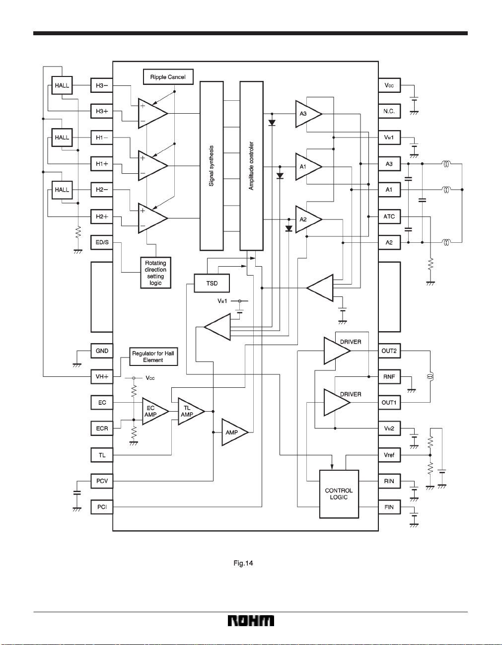
Block diagram
822
Page 3
Motor driver ICs BA6872AFM
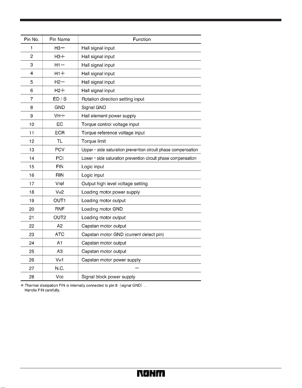
Pin descriptions
823
Page 4

Motor driver ICs BA6872AFM
Input/output circuits
(1) Hall inputs (pins 1 to 6)
(2) Rotation direction setting input (pin 7) (5) Torque limit (pin 12)
(4) Torque control input (pins 10 and 11)
(3) Hall element power supply (pin 9)
824
(6) Logic input (pins 15 and 16)
Page 5
Motor driver ICs BA6872AFM
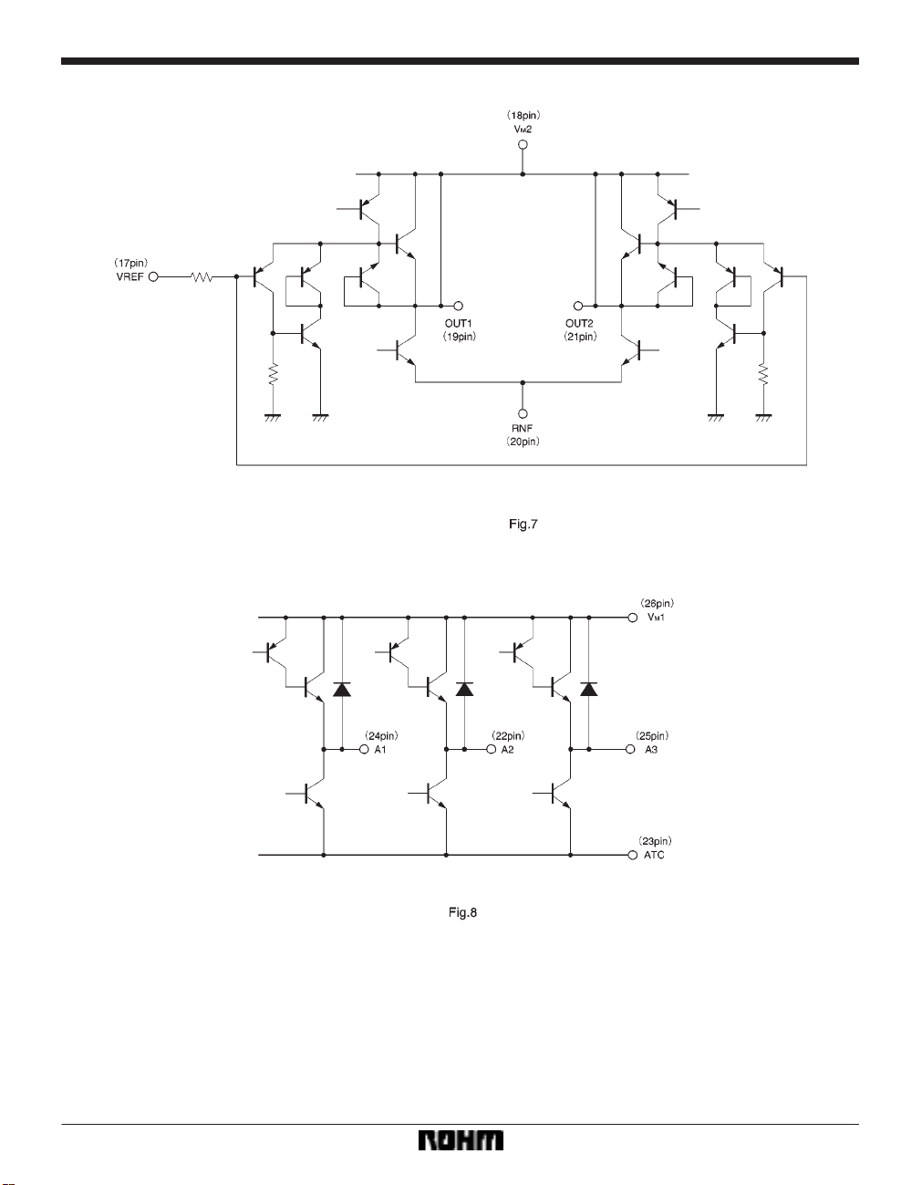
(7) Loading motor output (pins 17 to 21)
(8) Capstan motor output (pins 22 to 26)
825
Page 6
Motor driver ICs BA6872AFM
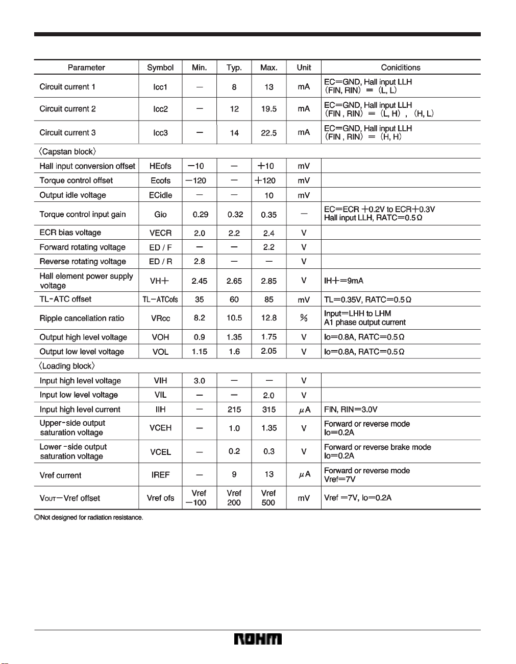
Electrical characteristics (unless otherwise noted, Ta = 25C, VCC = 5V, VM1 = 14V, VM2 = 14V)
826
Page 7
Motor driver ICs BA6872AFM
Circuit operation
Capstan three-phase motor driver
(1) Pseudo-linear output
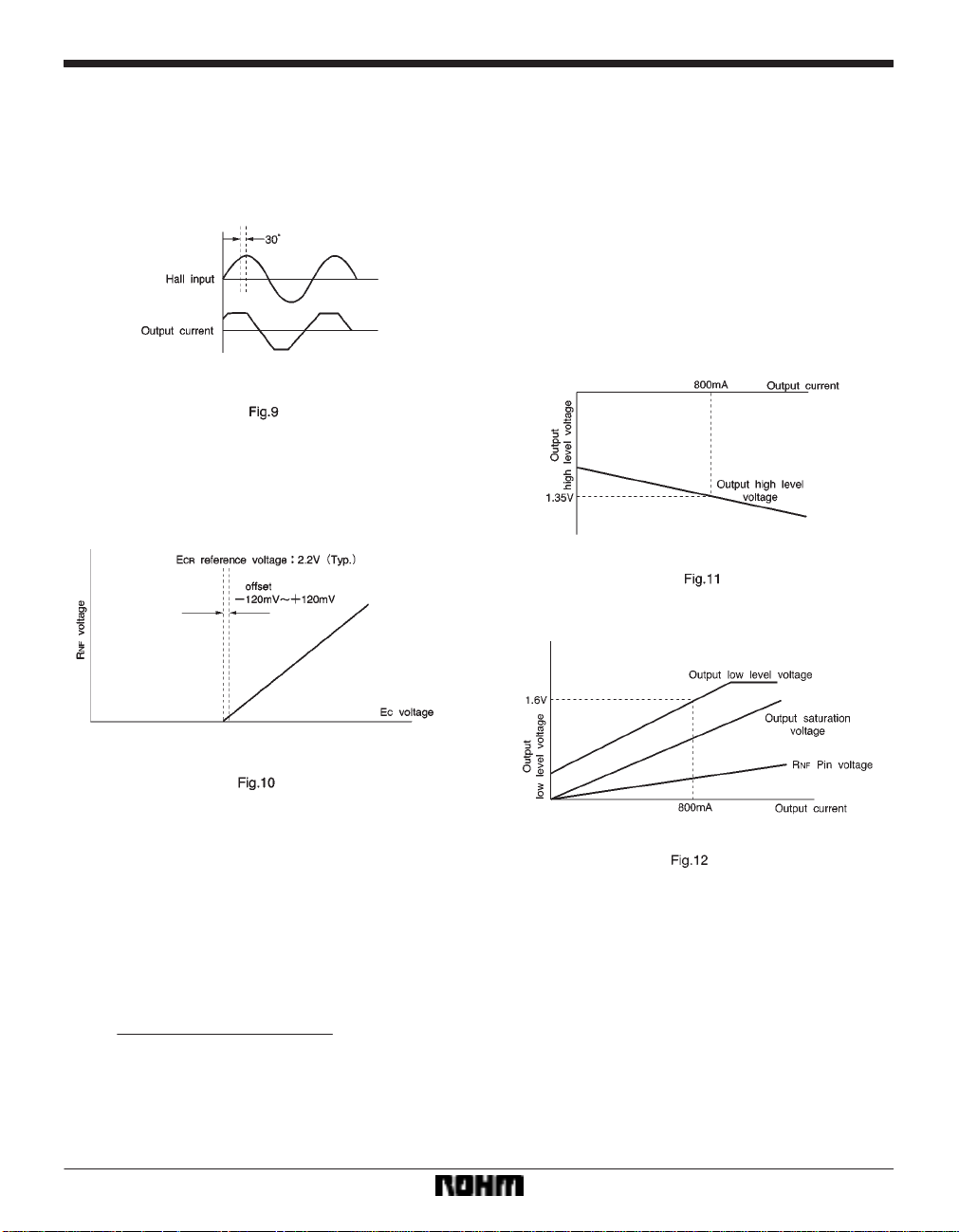
The IC generates a trapezoidal (pseudo-linear) output
current whose waveform phase is 30 degrees ahead of
that of the Hall input voltage.
(2) Torque control
The output current can be controlled by adjusting the
voltage applied to the torque control pins. The pins are
the inputs to a differential amplifier, and the reference
voltage side is biased with a voltage of 2.2V (Typ.).
(4) Motor direction control (ED/S pin)
The motor mode is forward when the ED/S is voltage is
less than 2.2V , and reverse when the ED/S is voltage is
greater than 2.8V.
(5) Output transistor saturation prevention circuit
This circuit monitors the output voltage and maintains the
operation of the output transistors below their saturation
levels. Operating the transistors in the linear characteristic range provides good control over a wide current
range, and good torque characteristics even during overload.
(3) Output current sensing and torque limiting
ATC (pin 23) is the output stage ground. Connect a small
resistor (0.5Ω recommended) between this pin and the
GND pin, and feedback the voltage drop across this resistor to the TL AMP input to detect the output current.The output current can be limited by adjusting the
voltage applied to TL (pin 12). The current is limited when
pin 12 reaches the same potential as pin 23. The output
current under this condition is given by:
IMAX. =
where RATC is the value of the resistor connected between the RA TC pin and ground, and VTL is the voltage
applied to the TL pin.
VTL – (TL – ATC offset)
RATC
827
Page 8
Motor driver ICs BA6872AFM
Reversible motor driver for loading
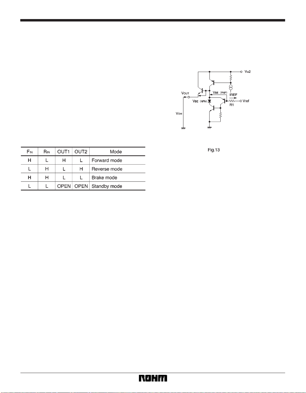
(6) Input block (F
IN and RIN) and mode explanation
These are the control signal input pins. The operations
of the various modes are explained below. When F
high level, and R
IN is low level, the mode is forward mode,
IN is
and current flows from OUT1 to OUT2.
IN is low level, and RIN is high level, the mode is
When F
reverse mode, and current flows from OUT2 to OUT1.
IN and RIN are both high level, the mode is brake
When F
mode. In brake mode, the upper-side output transistor is
off, and stops supply of current to the motor. The lowerside output transistor is on, and absorbs the back-rush of
the motor and applies braking. When F
IN and RIN are both
low level, OUT1 and OUT2 are open-circuit potential,
and the motor stops.
Truth table
(7) Vref pin (output high voltage setting pin)
The output voltage can be varied by controlling Vref.
V
OH = Vref VBE (PNP) VBE (NPN) (VOUT Vref off-
set) IREF R1
However, Vref V
M2 [Vsat (PNP) VBE (NPN)]
(8) Connection pins for output ground and output current sense resistor (RNF)
By connecting a resistor to this pin, it is possible to sense
the amount of current flowing in the motor. By adding an
electronic governor, and controlling V ref, it is possible to
construct a reversible motor driver.
828
Page 9
Motor driver ICs BA6872AFM
Application example
829
Page 10
Motor driver ICs BA6872AFM
Operation notes
(1) Thermal shutdown (TSD)
The BA6872AFM has a thermal shutdown circuit to protect the IC. The shutdown temperature is 175 C
(Typ.) and the hysteresis width is 65C (Typ.).
When the circuit is activated due to an increase in the
chip temperature, the output pins (pins 5, 6, and 9) are
set to the open state. This circuit is functional against excessive power dissipation, output short-circuiting, and
other irregularities in the output current, but does not
work against overheating caused by high internal currents due to externally-caused IC damage, or pin-to-pin
shorting.
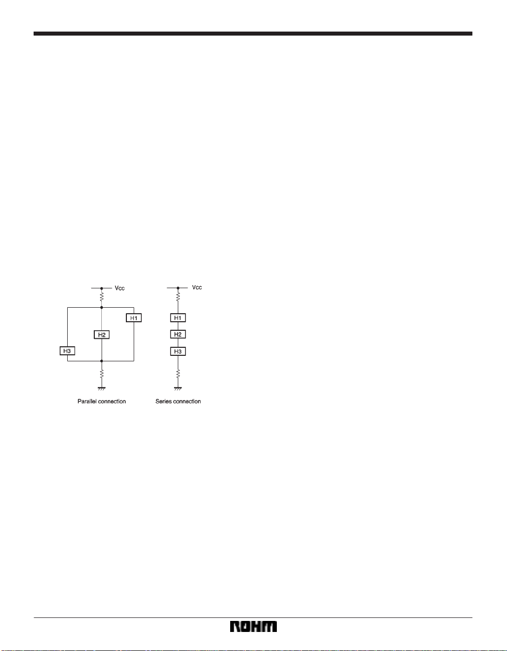
(2) Hall input
The Hall input circuit is shown in (1) on the I/O circuits.
Hall devices can be connected either in series or in parallel. Be sure to keep the Hall input within the range 1.5V
to (V
CC 1.8V).
(3) Setting pin for the output high-level voltage (Vref)
The voltage applied to the setting pin for the output highlevel voltage should not exceed the V
nect this to V
M2 when not using it.
M2 voltage. Con-
When the Vref pin is connected to a low impedance circuit for voltage setting, there is a chance that the output
voltage may oscillate.
When setting the voltage, set it via an impedance, or connect a capacitor between Vref and GND.
The impedance and capacitor values will differ depending on the motor type, PCB pattern, and load current, so
test the values using your actual circuit.
(4) GND
The GND (pin 8) potential must be kept below that of the
other pins at all times. The thermal dissipation FIN is internally connected to pin 8. T ake care regarding handling
of FIN.
(5) Input pins
Do not apply voltage to the inputs when V
supplied. Also, in the same way , even if V
plied, the inputs must be either at or below the V
CC is not being
CC is being sup-
CC level.
(6) Back-rush voltage
The back-rush voltage will vary depending on the operating conditions, environment, and motor characteristics.
T ake care to ensure that the back-rush voltage does not
interfere with the operation of the IC.
(7) Large current lines
Large currents flow in the power supply and GND lines
of this IC. Therefore, depending on the PCB pattern layout and the values of external circuit components connected between the power supply and GND such as capacitors, this large current can be returned to the input,
and cause incorrect operation and oscillation. To avoid
this, carefully check the PCB layout and the values of all
circuit components.
(8) The power dissipation of the IC depends on how it
is mounted. Perform thermal design carefully.
(9) Power consumption
The power dissipated by the IC varies widely with the applied voltage and output current. Pay close attention to
the allowed power dissipation, and base your thermal design on the thermal resistance data and transient thermal
resistance data to ensure that the ratings are not exceeded.
(10) ASO
Make sure that the output current and supply voltage do
not exceed the ASO values.
(11) Input mode switching
T o improve reliability , when switching modes, first switch
to the open mode.
830
Page 11
Motor driver ICs BA6872AFM
(12) This IC is not equipped with a circuit to limit in-rush
current. Therefore, connect a current limiting resistor to
limit the in-rush current.
(13) Depending on the thermal dissipation conditions,
power supply voltage, and type of motor, the potentials
on the output pins of this IC can swing to levels well below
GND, and cause faulty operation. In this case, take appropriate countermeasures such as connecting a diode
between the outputs and GND.
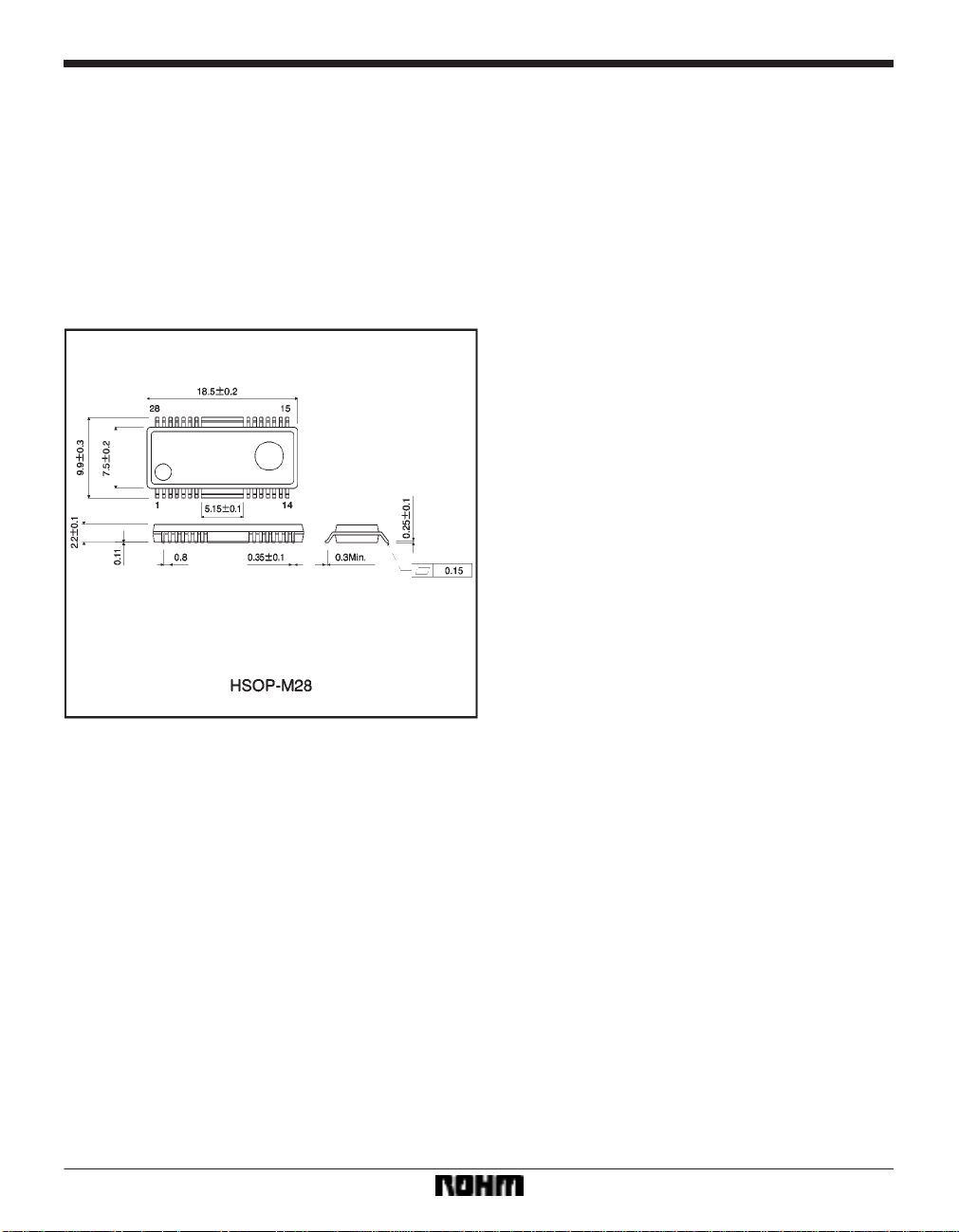
External dimensions (Units: mm)
(14) Great care has been paid to the quality of this component. However, if the absolute maximum ratings for
temperature and applied voltage are exceeded, the IC
may be destroyed. Since it is not possible to predict
whether the IC will be in the short mode or open mode if
it is destroyed, be sure to use sufficient physical protective measures (fuses etc.) if there is a chance that the
maximum ratings of the IC will be exceeded.
831
 Loading...