

Page 1
Optical disc ICs
4-channel BTL driver for CD players
BA6898S / BA6898FP
The BA6898S / BA6898FP ICs contain a 4-channel BTL driver , 5V regulator (which requires an externally connected
PNP transistor), multi-purpose operational amplifier, and reset output for use with CD players. Also equipped with an
input pin for gain adjustment for all channels of the driver block so that the gain can be adjusted to the desired value
for your application. Furthermore, a built-in level shift circuit exists to further reduce the amount of external components
required.
Applications
CD players, CD-ROM, and other optical disc equipment
Features
1) 4-channel BTL driver.
2) Gain is adjustable with externally connected resistor.
3) Internal thermal shutdown circuit.
4) Internal 5V regulator (requires external PNP transistor).
5) Internal multi-purpose operational amplifier.
6) Equipped with reset output pin.
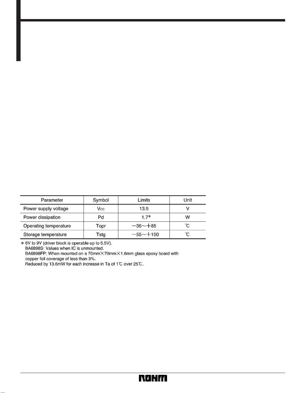
Absolute maximum ratings (Ta = 25C)
671
Page 2
Optical disc ICs BA6898S/BA6898FP
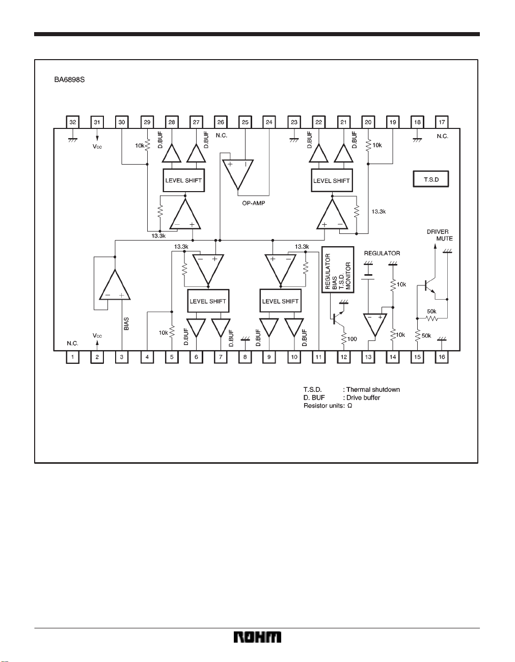
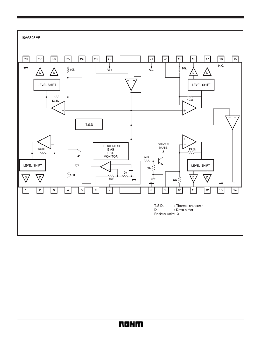
Block diagram
672
Page 3
Optical disc ICs BA6898S/BA6898FP
673
Page 4
Optical disc ICs BA6898S/BA6898FP
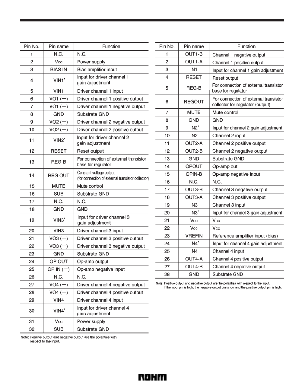
Pin descriptions
BA6898S BA6898FP
674
Page 5

Optical disc ICs BA6898S/BA6898FP
Input / output circuits
675
Page 6

Optical disc ICs BA6898S/BA6898FP
Electrical characteristics (unless otherwise noted, Ta = 25C, VCC = 8V, f = 1kHz, RL = 8Ω)
676
Page 7

Optical disc ICs BA6898S/BA6898FP
Measurement circuit
677
Page 8

Optical disc ICs BA6898S/BA6898FP
Circuit operation
(1) Driver block
The input is the focus and tracking error signals from the
servo pre-amplifier and the control signals for the motor
system. The input signal is normally centered at 2.5V,
and at the pre-amplifier, it undergoes V / I conversion to
generate the current corresponding to the input voltage.
This is then passed through a resistor and sent to the internal reference voltage block.
This results in the output from the pre-amplifier being the
signal at the center of the internal reference voltage.
Furthermore, at the V / I conversion, forward and reverse
phases are generated and the BTL output is then gained
through the driver buffer.
(2) Regulator block
The configuration is that of a normal series-type regulator
and the reference voltage is provided internally. A PNP
low-saturation transistor is connected externally.
678
Page 9

Optical disc ICs BA6898S/BA6898FP
Application example
679
Page 10

Optical disc ICs BA6898S/BA6898FP
Operation notes (pin Nos. are those for the BA6898S)
(1) Relationship between mute and reset output
Regulator voltage drop If the regulator voltage drops to 4.0V (Typ.) or below, the reset output turns low and the. . . . .
mute turns on. If the voltage then rises again to 4.2V (Typ.), the reset output turns high
and the mute turns off.
Bias voltage drop If the bias pin (pin 3) voltage lowers to 1.4V (Typ.) or below, the mute turns on and the. . . . . . . . . .
reset output turns low. For normal operations, have the voltage at 1.6V or greater.
Thermal shutdown When the chip temperature reaches 175C (Typ.), the mute turns on and the reset output. . . . . . . . .
turns low. If the chip temperature then drops below 150C (T yp.), then the mute turns off
and the reset output turns high.
Mute (pin 15) If the mute pin (pin 15) voltage is open or lowers to 0.5V or below, the mute turns on but. . . . . . . . . . . . .
the reset output does not change.
(2) If the voltage of the thermal shutdown, mute ON, or
bias pin drops, or if the regulator voltage drops, the mute
is activated; however, in these situations, only the drivers
are muted. Also, the output pin voltage becomes the internal bias voltage (approx. (V
CCVF) / 2).
(3) Connect a bypass capacitor (approx. 0.1µF) between the bases of the power supply pins of this IC.
(4) Even though pins 16 and 32 are connected to
ground within the package, be sure to also connect them
to a ground externally as well.
Electrical characteristic curves
(5) The capacitor connected between the regulator
output pin (pin 14) and GND also serves to prevent oscillation, so be sure to use a capacitor with excellent thermal characteristics.
(6) If the regulator is not used, short the regulator output pin (pin 14) to V
CC and have the pin for the externally
connected transistor base (pin 13) open.
(7) Of the ground pins, only pin 18 is not connected to
the IC substrate. Therefore, design the PC board pattern
so that the potential of GND pin 18 does not go below the
substrate GND (including transient conditions).
680
Page 11

Optical disc ICs BA6898S/BA6898FP
External dimensions (Units: mm)
681
 Loading...