

Page 1
Motor driver ICs
3-phase motor driver for
CD-ROMs
BA6848FP / BA6853FS
The BA6848FP and BA6853FS are single-chip ICs developed for CD-ROM spindle motor drives. These ICs are 3phase, full-wave, pseudo-linear drives with FG output, FG composite output, and reverse-rotation pins built-in for high
functionality and high performance.
Applications
CD-ROM, CD-R, CD-RW, DVD-ROM, DVD-RAM
Features
1) Three-phase, full wave, pseudo-linear drive system.
2) Built-in PS pin for power save mode when ON.
3) Built-in thermal shutdown and current limiter circuits.
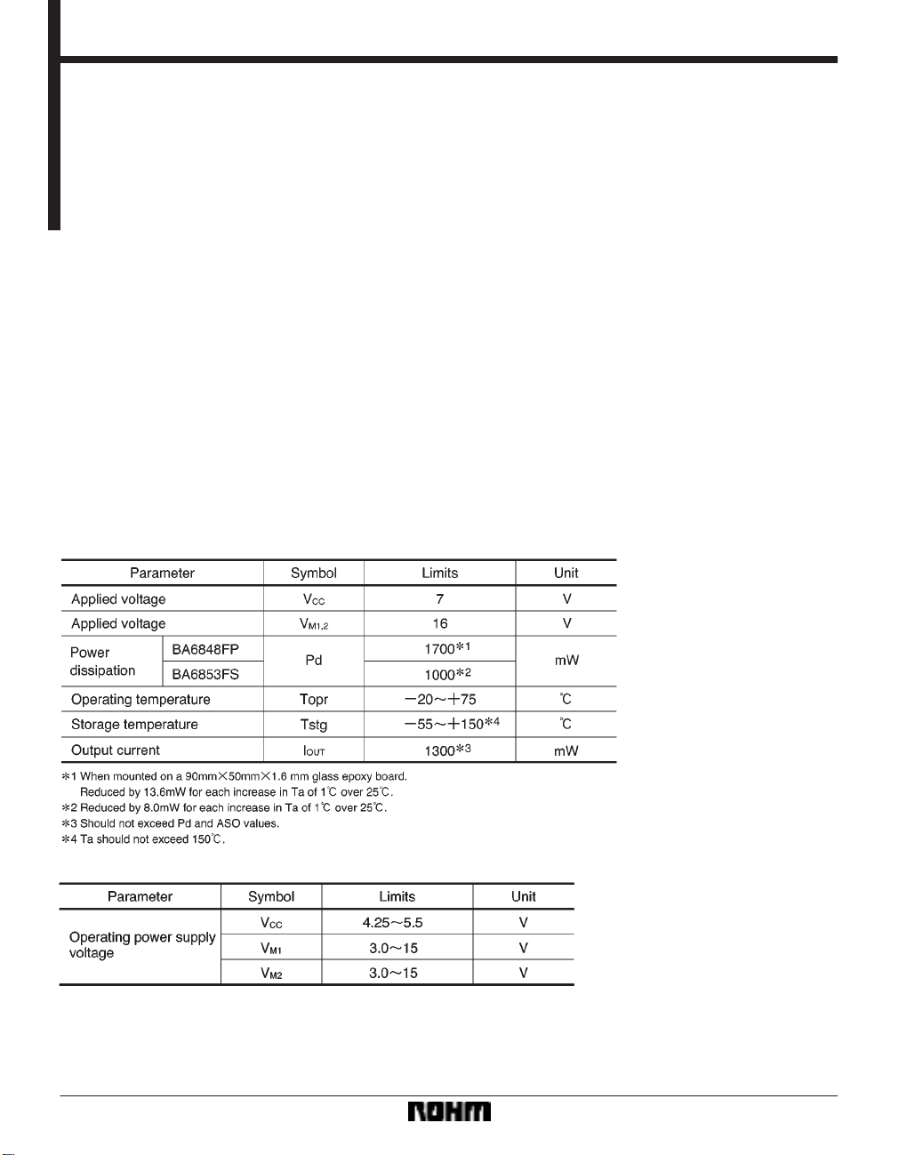
Absolute maximum ratings (Ta = 25C)
4) Built-in Hall bias circuit (for the BA6848FP).
5) Built-in FG output and FG composite output.
6) Built-in reverse-rotation pin.
Recommended operating conditions (Ta = 25C)
781
Page 2
Motor driver ICs BA6848FP / BA6853FS
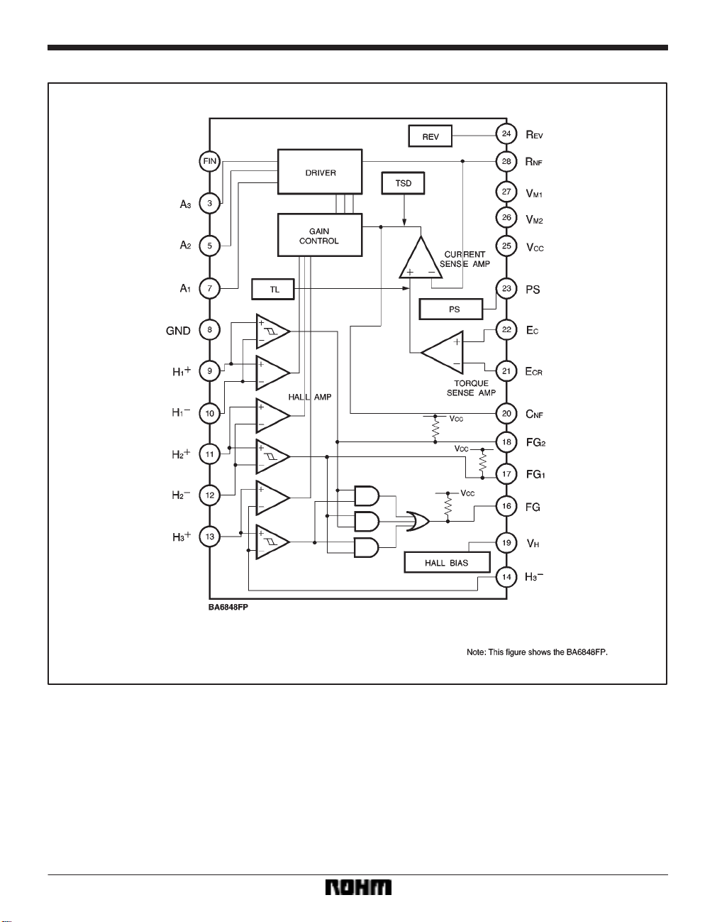
Block diagram
782
Page 3
Motor driver ICs BA6848FP / BA6853FS
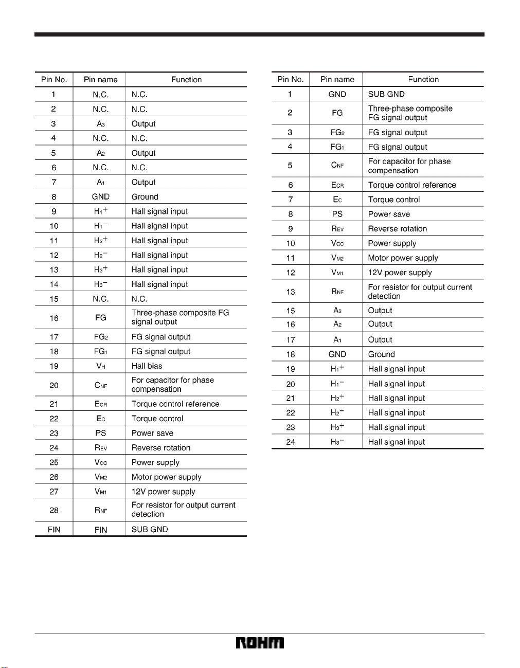
Pin descriptions
BA6848FP BA6853FS
783
Page 4
Motor driver ICs BA6848FP / BA6853FS
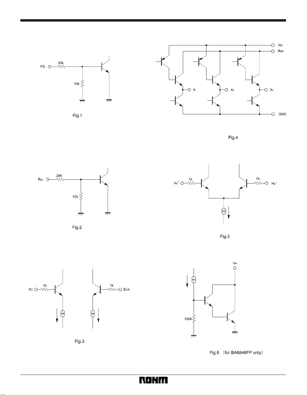
I / O circuit diagrams
(1) Power save(PS)
(4) Coil output (A1, A2, A3)
(2) Reverse (REV)
(3) Torque command input (6) Hall bias
(5) Hall input
(H1
, H1, H2, H2, H3, and H3)
784
Note: Resistances are typical values.
Page 5

Motor driver ICs BA6848FP / BA6853FS
Electrical characteristics (unless otherwise noted, Ta = 25C, VCC = 5V, VM1 = 12V, VM2 = 12V)
785
Page 6

Motor driver ICs BA6848FP / BA6853FS
Circuit operation
(1) Hall input and output
The phase relationship between the Hall input signals and the output current and voltage is shown below in Fig.7. The
input three-phase Hall signal is sent to the matrix section for waveform synthesis. This signal is input to the output driver
and supplies the drive current to the motor coil.
786
Page 7

Motor driver ICs BA6848FP / BA6853FS
(2) Torque command
NF pin voltage with respect to the torque command
The R
C) is as follows:
(E
The I / O gain G
EC from EC pin to RNF pin (output current)
is determined by the R
EC = 0.255 / RNF [A / V]
G
The torque limit current I
TL = 0.35 / RNF [A]
I
NF detector resistance.
TL is:
787
Page 8

Motor driver ICs BA6848FP / BA6853FS
(3) FG signal output waveform
From the Hall input signal, a pulse signal (FG signal) is output proportional to the motor speed of rotation. This timing
is shown in Fig.9 below.
(4) Other
For the PS pins, the circuits turn on at 3.5 V or greater, and enter the power save mode at 1.5 V or less. For the R
it enters the reverse mode at 4.0 V or greater, and enters the normal mode at 1.5 V or less.
788
EV pin,
Page 9

Motor driver ICs BA6848FP / BA6853FS
Application example
789
Page 10

Motor driver ICs BA6848FP / BA6853FS
Operation notes
(1) Power save
The power save input is an input / output circuit as
shown in Fig.1. The power save pins have a thermal derating characteristic of 8mV / C. The resistance also
has a fluctuation of ±30%, so be careful of the input voltage range.
(2) Reverse
The reverse input is an input / output circuit as shown in
Fig.2. The reverse pins have a thermal derating characteristic of 7mV / C. The resistance also has a fluctua-
tion of ±30%, so be careful of the input voltage range.
(3) Hall input
The Hall input is an input circuit as shown in Fig.5. The
Hall elements can be connected in series or in parallel.
(4) Thermal shutdown (TSD)
When the junction temperature reaches 175C (Typ.),
the A
1 to A3 coil outputs become open. There is an
approximate 15C (Typ.) temperature hysteresis.
790
Page 11

Motor driver ICs BA6848FP / BA6853FS
Electrical characteristic curves
External dimensions (Units: mm)
791
 Loading...