

Page 1
Motor driver ICs
Spindle and loading motor driver for PD
BA6852FP
The BA6852FP is a motor driver IC developed for use in PD, CD-ROM and DVD applications. In addition to having a
conventional spindle motor driver, it includes a reversible motor driver for use with loading motors to allow easy system
construction.
Applications
PD, CD-ROM and DVD.
Features
1) Power save circuit (three-level switch) allows FG output in power save mode.
2) FGSW allows selection between either three-phase
composite output or single-phase output for the FG
output.
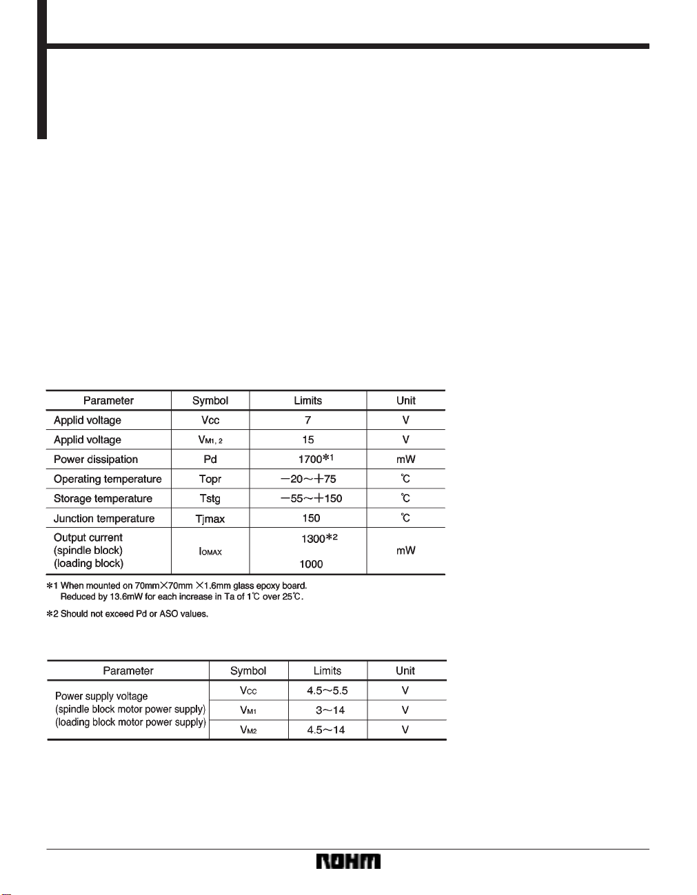
Absolute maximum ratings (Ta = 25C)
3) The output voltage for the loading motor driver can be
set using the Vref pin.
Recommended operating conditions (Ta = 25C)
792
Page 2
Motor driver ICs BA6852FP
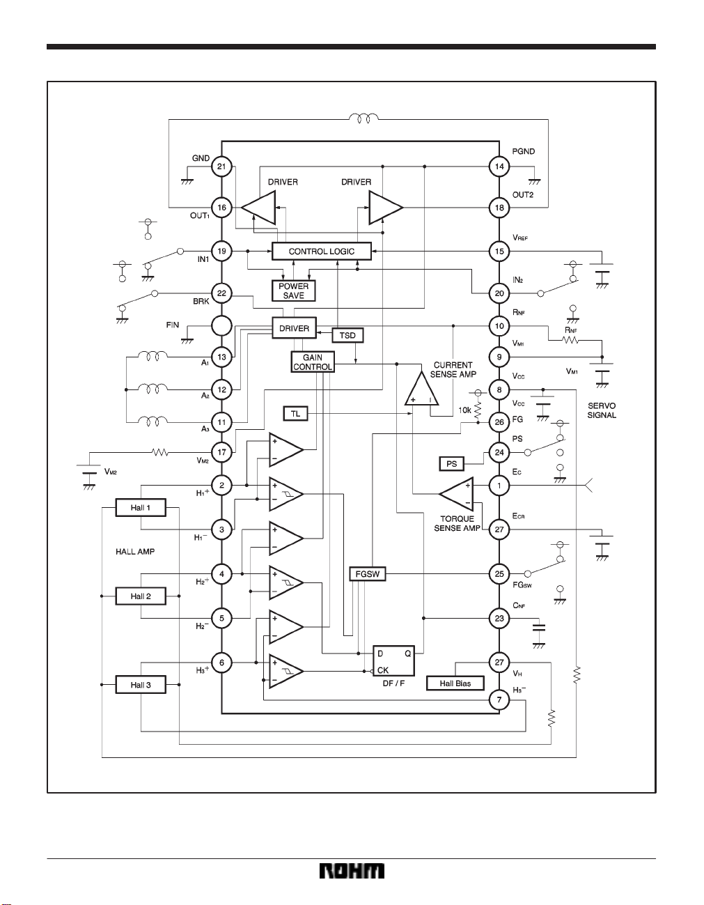
Block diagram
793
Page 3
Motor driver ICs BA6852FP
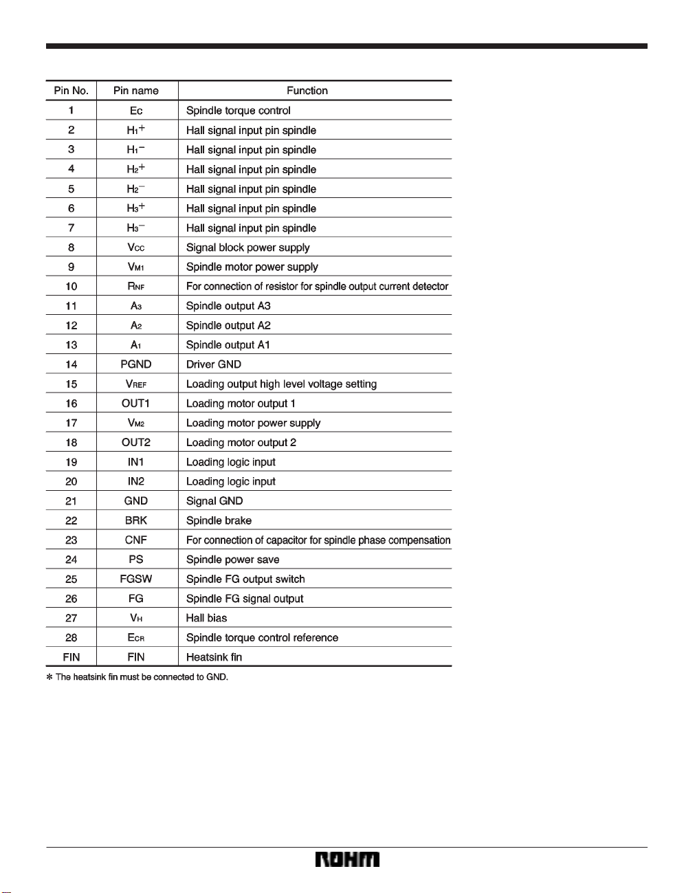
Pin descriptions
794
Page 4
Motor driver ICs BA6852FP
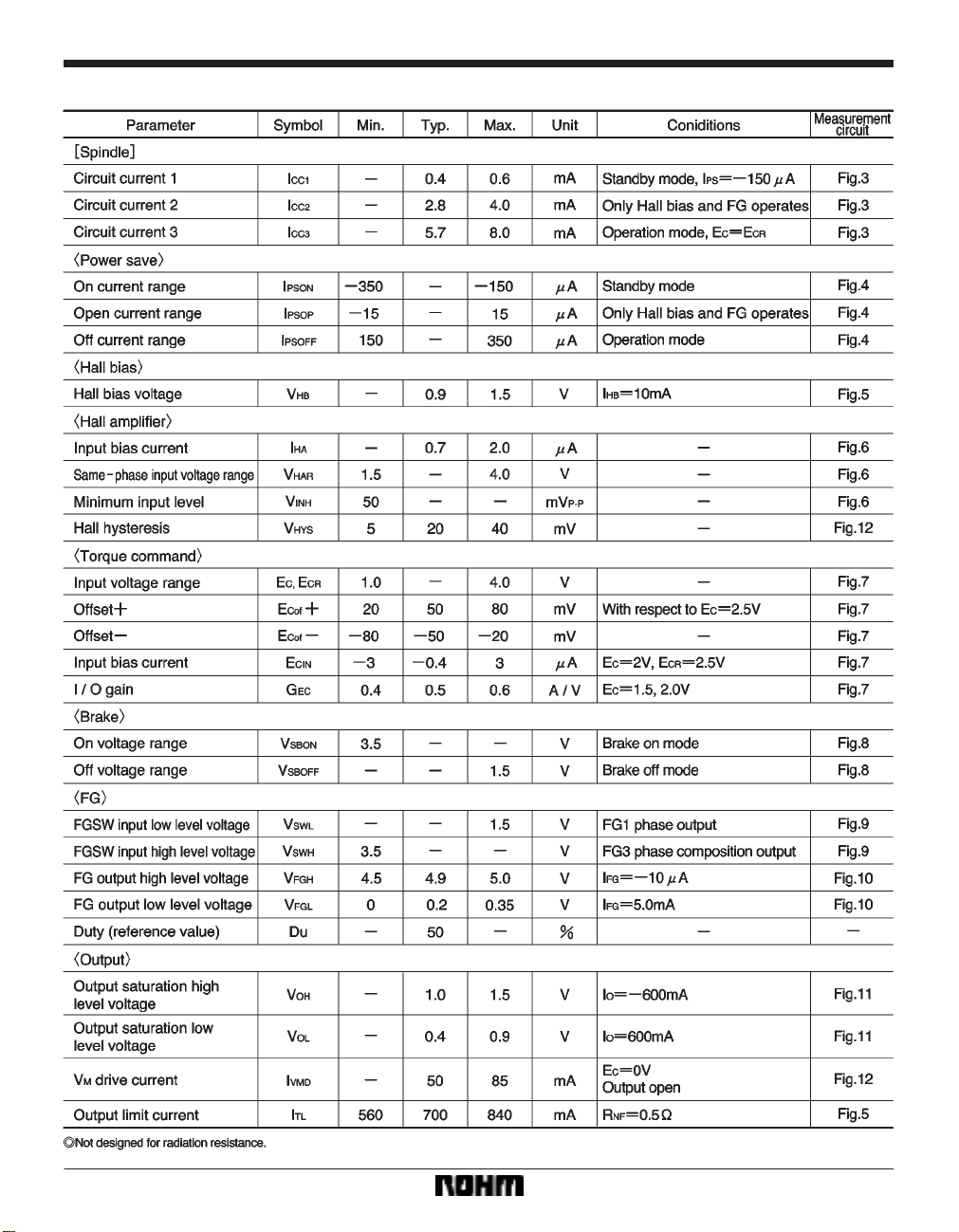
Electrical characteristics (unless otherwise noted, Ta = 25C, VCC = 5V, VM1 = 12V, and VM2 = 12V)
795
Page 5

Motor driver ICs BA6852FP
Measurement circuits
(1) Measurement circuit resistance
(2) Input/output table
Note: Forward E
Reverse EC > ECR
C < ECR
796
Input voltage H = 2.6V
M = 2.5V
L = 2.4V
Page 6

Motor driver ICs BA6852FP
(3) Measurement circuits
ICC1 : Ammeter A1 value
IPS1 = 150µA
H
1
, H2, H3 = VCC / 2 (V)
1
, H2, H3 = VCC /2 0.1 (V)
H
CC2 : Ammeter A1 value
I
PS = OPEN
1
, H2, H3 = VCC / 2 (V)
H
H
1
, H2, H3 = VCC /2 0.1 (V)
CC3 : Ammeter A1 value
I
IPS3 = 150µA
1
, H2, H3 = VCC / 2 (V)
H
1
, H2, H3 = VCC /2 0.1 (V)
H
I
PSON
IPS range for which all output pins
:
are open
(input conditions 1 to 6)
PSOP
IPS range for only FG and the hall
I
:
bias operate
(input conditions 1 to 6)
I
PSOFF
PS range for which the output pins
:
are as in the Input / output table
(input conditions 1 to 6)
797
Page 7

Motor driver ICs BA6852FP
VHB : Voltmeter V1value
VPS = 5V
IHB = 10mA
I
TL : (Voltmeter V2value) / 0.5
VPS = 5V
C = 0V
E
(input conditions 1 to 6)
HA : With Hn
I
the current that flows into Hn
With Hn
the current that flows into Hn
= 4.0V, Hn = 2.5V,
= 2.5V, Hn = 4.0V,
(n = 1, 2, 3)
HAR : Hall input voltage range for which
V
the output pin is as per the Input /
output table.
INH : Hall input level for which the output
V
pin is as per the Input / output table.
| Hn
Hn l Hin = 2.5V
798
Page 8

Motor driver ICs BA6852FP
EC, ECR : Torque command operation
voltage range
E
COF± : Vary EC until ECR = 2.5V, then
C voltmeter V1 < 3mV.
Vary E
C voltage range
This E
(see operation notes (2)).
CIN : Ammeter value when
E
C = 2V and ECR = 2.5V
E
EC : If the V1 value is V2 when
G
C = 1.5V, and the V1
E
value is V3 when E
EC = {(V2 V3) / (2.0 1.5)} /
G
NF (RNF = 0.5Ω)
R
C = 2.0V
V
SBON : BRK pin voltage range when all
output pins are low.
SBOFF : BRK pin voltage range when all
V
output pins are as per the Input /
output table.
799
Page 9

Motor driver ICs BA6852FP
VSWL : FGSW pin voltage range when
the hall input and FG output are
as per the table below.
V
SWH : FGSW pin voltage range when
the hall input and FG output are
as per the table below.
800
V
FGH : Voltmeter V1 value
(Input / output table, condition 2)
IFG = 10µA
FGSW = 0V
FGL : Voltmeter V1 value
V
(Input / output table, condition 1)
IFG = 3mA
FGSW = 0V
Page 10

Motor driver ICs BA6852FP
VOH : With the output measurement pin
made high level according to the
input conditions, the V1 value when
600mA flows from that pin.
V
OL : With the output measurement pin
made low level according to the
input conditions, the V2 value when
600mA flows from that pin.
VHYS : The voltage difference V3 between
1
and H1 that switch the FG pin.
H
E
C = 2.5V
FGSW = 0V
VMD : Ammeter A1value
I
Output open (input conditions 1 to 6)
C = 0V
E
801
Page 11

Motor driver ICs BA6852FP
ICC4 : Ammeter A1 value
IN1 = 5V, IN2 = 0V
I
CC5 : Ammeter A1 value
IN1 = 5V, IN2 = 5V
IH : IN1 range for which OUT1 = High,
V
OUT2 = Low (IN2 = Low)
IN2 range for which OUT1 = Low,
OUT2 = High (IN1 = Low)
V
IL : IN1 range for which OUT1 = Low,
OUT2 = High (IN2 = High)
IN2 range for which OUT1 = High,
OUT2 = Low (IN1 = High)
I
IH : Ammeter A2 value when IN1 = 2V
Ammeter A3 value when IN2 = 2V
CE : Sum of V1 (the value when 200mA is
V
flowing from the output high level pin)
and V2 (the value when 200mA is
flowing to the output low level pin).
802
Page 12

Motor driver ICs BA6852FP
IREF : Ammeter A1 value
O = 100mA
I
V
REF = 9V
REF :VREF pin voltage range for which the
V
output voltage can be controlled
Operation notes
(1) Torque command
NF pin voltage with respect to the torque command
The R
input (EC) is as follows.
The I / O gain GEC from the EC pin to the RNF (output
current) is determined by the R
NF detector resis-
tance.
G
EC = 0.25 / RNF (A / V)
The torque limit current I
I
TL = 0.35 / RNF (A).
TL is given by
803
Page 13

Motor driver ICs BA6852FP
(2) Power save
The power save pin logic is as follows.
(3) Reverse rotation detector
The construction of the reverse rotation detector circuit
is shown in Fig. 17.
(1) Forward (EC < ECR)
The phase relationship between the hall input sig-
2
nals H
verse rotation detector circuit does not operate.
(2) Reverse (E
The phase relationship between H
opposite to that for forward rotation, and the reverse rotation detector circuit operates to switch the
output off and leave it in the open state.
and H3 is as shown in Fig.18, and the re-
C > ECR)
2
and H3 is
804
Motor operation during reverse detection
When EC < ECR, forward rotation (right rotation)
When EC > ECR, reverse torque is applied to reduce speed (right rotation)
When the motor reverses, the reverse rotation detector operates, and the coil output is opened.
Free rotation in the reverse direction by inertia.
Stop
Page 14

Motor driver ICs BA6852FP
(4) Input / output timing chart (forward rotation)
805
Page 15

Motor driver ICs BA6852FP
(5) Short brake
When the BRK pin goes to high level, the upper-side output transistors (three phase) go off, and the lower-side output
transistors (three phase) go on.
(6) Hall input
The hall pins can be connected in series or parallel.
806
Page 16

Motor driver ICs BA6852FP
(7) FG output switch
The relationship between the FG output switch pin and
the FG output is as follows.
(8) About the input pin applied voltage
Do not apply voltage to any of the other pins when the V
voltage is not being supplied to the IC. In addition, when
CC is being applied, do not apply a voltage more than VCC
V
to any of the other pins.
(9) Input pins
The loading input pin has a negative temperature characteristic, so when using it, give due consideration to the
temperature characteristics.
(10) V
REF pin (output high level voltage setting)
The loading block output high level voltage can be set using the V
The output high level voltage V
REF pin voltage.
OH is given by the following
formula.
V
OH = VREF ) IREF R1 ) VBE (Q1) – VBE (Q3)
REF voltage that brings about the above formula is
The V
M2 – VCE (Q2) – VBE (Q3).
up to V
Do not apply a voltage of more than V
Short the V
CC
REF pin to VM2 if you will not use it.
M2 to the VREF pin.
807
Page 17

Motor driver ICs BA6852FP
(11) Spindle and loading operation conditions
When IN1 or IN2 are high level, the spindle is off regardless of the PS pin input.
(12) Driver section ground (GND)
PGND (pin 14) is the driver section GND, and is not connected to the signal section GND. This is the motor current path, so take care with the PCB track width and arrangement on the PC board.
Electrical characteristics curves
(13) Thermal shutdown (TSD)
When the junction temperature reaches 175C (Typ.),
the motor output is opened. There is approximately 15C
(Typ.) of temperature hysteresis.
808
Page 18

Motor driver ICs BA6852FP
External dimensions (Units: mm)
809
 Loading...