

Page 1

Audio ICs
LED level meter driver, 12-point 2
channel, VU scale, bar display
BA6820F / BA6822S / BA6822F
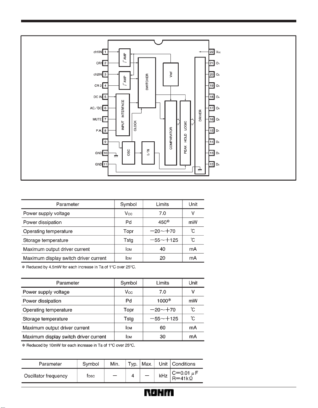
The BA6820F, BA6822S and BA6822F are two-channel, 12-point LED drivers for VU-scale bar-level meters.
The ICs are available in 22-pin SOP (BA6820F and BA6822F) and 22-pin shrink-DIP (BA6822S) packages, and use
a dynamic-drive system that can drive two 12-point displays. The ICs have independent AC and DC inputs, and the AC
input mode has a peak hold circuit (with cancel function). The ICs also feature a power-on mute, so steps to prevent
erroneous LED lighting at power on are not required.
The input resistance of the AC inputs is 3kΩ (Typ.) for the BA6820F and 0.3kΩ (Typ.) for the BA6822S/F.
Applications
Level meters for VCRs, stereo cassette players, audio
amplifiers and karaoke equipment.
Features
1) Uses dynamic-drive system to display two 12-point
channels. 22-pin SOP and 22-pin shrink DIP packages.
2) Independent AC and DC inputs provided (one input
displays one channel). Switching function allows
two-mode display .
3) Upper 8 points have peak hold function in AC mode
(two seconds). A peak-hold cancel function is also
provided.
4) A mute function is provided, and muting can be applied externally .
5) Power on mute function.
662
Page 2
Audio ICs BA6820F / BA6822S / BA6822F
FBlock diagram
FAbsolute maximum ratings
(BA6820F/BA6822F) (Ta = 25_C)
(BA6822S) (Ta = 25_C)
FRecommended operating conditions (Ta = 25_C)
663
Page 3
Audio ICs BA6820F / BA6822S / BA6822F
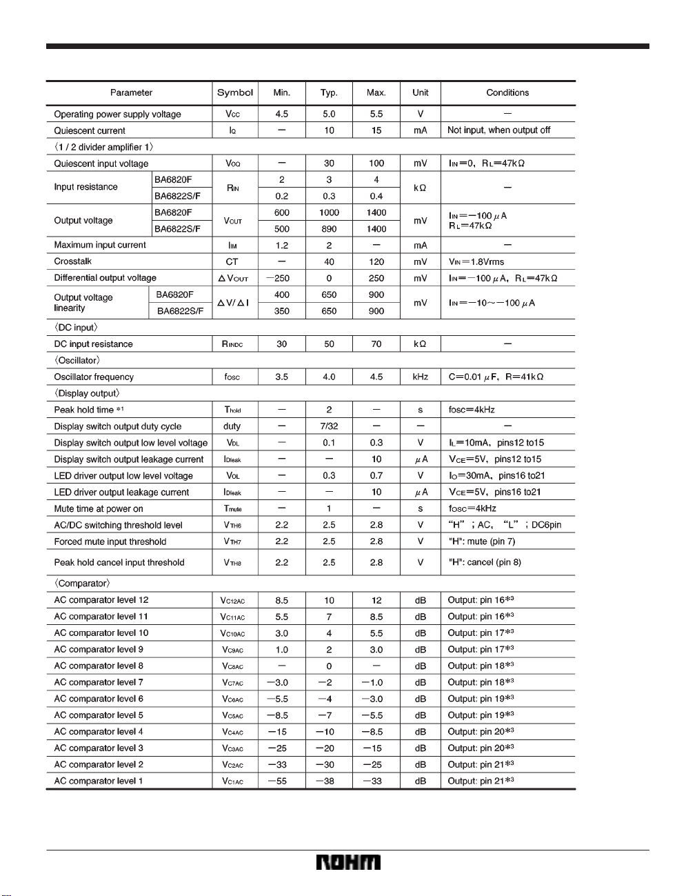
FElectrical characteristics (unless otherwise noted, Ta = 25_C, VCC = 5.0V and f = 1kHz)
664
Page 4

Audio ICs BA6820F / BA6822S / BA6822F
665
Page 5

Audio ICs BA6820F / BA6822S / BA6822F
Measurement circuit
Application example
666
Page 6

Audio ICs BA6820F / BA6822S / BA6822F
FAttached components
S C1 and C2: 1µF input coupling capacitors (electrolytic)
for the square-root compression amplifier. The rectified
voltage output from pins 2 and 4 is attenuated by 1.5dB
at the frequency determined by the following formula (refer to the data for the relationship between the pin 2 and
4 DC voltage frequency characteristics and the LED
lighting level).
fC = (R
2π
1
S C1 (RIN)VR1)
IN = input resistance)
When the LEDs light due to low-frequency mechanical
noise or induced hum, reduce the values of C
1 and C2
to cut the cut the low-frequency frequency characteristic.
1 and VR2: 5kΩ to 100kΩ potentiometers for sen-
S VR
sitivity and L/R balance adjustment (refer to item 2 of
Circuit operation).
S C
3 and C4: 22µF electrolytic capacitors.
1 and R2: 47kΩ carbon-film resistors.
S R
These resistors set the attack and release times (refer
to item 6 of the Circuit operation).
5: 0.01µF mylar capacitor.
S C
R
3: 39kΩ carbon-film resistor.
This resistor sets the oscillator frequency (refer to the
Operation notes).
6: 100µF electrolytic capacitor. This capacitor is
S C
used as a ripple filter. The positive lead should be connected close to V
CC (pin 22), and the negative lead
close to the junction of pins 10 and 1 1.
S Q
1 to Q4: 2SA854S Transistors for display switching.
If the current for one LED is I
LED, the values of IC and PC
for each of Q1 to Q4 when all LEDs are lit are given by:
C = 6 ILED (for duty cycle of 7/32)
I
P
C = 6 ILED Vsat
7
32
Choose transistors that have sufficient margin for I
P
C.
4 to R7: 2.2kΩ carbon-film resistors.
S R
These resistors limit the base current for transistors Q
to Q2. The base current is the collector current divided by
FE, but as the transistors are operated in the saturation
h
region, h
FE will drop considerably. Choose the resistors
so that sufficient base current flows.
S LED
1 to LED12: SLB-26
8 to R13: 330Ω carbon-film resistors. These resistors
S R
set the LED current. Four LEDs are connected to each
resistor, but as the LEDs light sequentially, only the current for one LED flows in a resistor.
R8X13 =
V
DL = Display switch output “L” voltage.
VCC*VLED*Vsat (Q1*Q4) *VDL
ILED
C and
1
FCircuit operation
(1) Function
There are 12 LEDs each for the left and right channels,
and these are divided into 4 groups of six. A dynamicdrive technique is used to drive the LEDs in order, and
provide 12 display points for each channel. A 12-point
VU-scale bar display is produced over the display range
*38dB to +10dB. The top eight points have a peak hold
function which may be cancelled if required (there is no
peak hold function for DC mode).
Independent AC (two channels) and DC (one channel)
inputs are provided, and a control input pin is used to
switch between them.
In DC mode, only channel 2 operates.
A power-on mute circuit is provided, so no measures are
required to prevent erroneous lighting of the LEDs when
power is applied.
The attack and release times for the display can be set
using external components.
(2) Input block (pins 1, 3 and 5)
Pins 1 and 3 are the AC inputs, and pin 5 is the DC input.
Pin 6 is used to switch between AC and DC input. When
the pin 6 input is “H”, AC input is selected (pins 1 and 3),
and when it is “L”, DC input (pin 5) is selected. Therefore,
if pins 1 and 3 are used for audio input, and pin 5 as the
input for signal meter output (DC) from a tuner, the switch
input (pin 6) can be used to make LED display do two
jobs.
Pins 1 and 3 have low input impedance, so we recommend that you connect potentiometers (VR
1 and VR2:
5kΩ to 100kΩ) in series with the inputs to adjust the balance between ch1 and ch2 and set the levels.
667
Page 7

Audio ICs BA6820F / BA6822S / BA6822F
(3) Peak hold
The peak hold circuit momentarily holds the maximum
signal level in AC input mode. The peak hold function applies to comparator levels 5 to 12 (8 points). When the oscillator frequency is 4kHz, the peak hold time is two seconds (Typ.), and can be changed by changing the
oscillator frequency. The peak hold function can be
turned off by setting pin 8 high.
The peak hold function does not operate in DC input
mode.
(4) Output block
The two sets of 12 LEDs for the BA6820F and
BA6822S/F are divided into 4 groups of six. A dynamicdrive technique is used to drive the LEDs in order, and
display the input level.
Group 1
Channel 1 LEDs 1, 3, 5, 7, 9 and 11
(odd-numbered LEDs)
Group 2
Channel 1 LEDs 2, 4, 6, 8, 10 and 12
(even-numbered LEDs)
Group 3
Channel 2 LEDs 1, 3, 5, 7, 9 and 11
(odd-numbered LEDs)
Group 4
Channel 2 LEDs 2, 4, 6, 8, 10 and 12
(even-numbered LEDs)
Therefore, six LED drive outputs, and four display switch
terminals are provided.
The output timing chart for when all LEDs are lit is shown
in Fig. 3.
In DC input mode, only channel 2 operates.
D
1 to D4 in the timing chart operate in the same way as
for AC mode (i.e. D
1 and D2 operate), but O1 to O6 are high
for the channel 1 period.
(1) Display switch outputs (pins 12 to 15)
To successively switch between the four LED groups,
these outputs are active low (see Fig. 4).
The outputs are pulled up by 36kΩ resistors (between the
base and emitter of Q
1 to Q4), so leak current bypass re-
sistors are not required.
668
Page 8

Audio ICs BA6820F / BA6822S / BA6822F
(2) LED drive outputs (pins 16 to 21)
These are open-collector outputs that drive the LEDs
(see Fig. 5).
One complete cycle of the timing chart starting from O
(pin 21) is as follows: if the channel 1 input is higher than
comparator level 1 during the first-point period for channel 1, a “L” level is output. Next, if the channel 1 input is
higher than comparator level 2 during the second-point
period for channel 1, a “L” level is output, if the channel
2 input is higher than comparator level 1 during the firstpoint period for channel 2, a “L” level is output, and then
if the channel 2 input is higher than comparator level 2
during the second-point period for channel 2, a “L” level
is output.This cycle is then repeated for outputs O
2 to O6.
(5) Mode switch pins (pins 6, 7 and 8)
S AC/DC mode switch pin (pin 6)
When “H” AC input (pins 1 and 3) is selected, and when
“L” DC input (pin 5) is selected.
“H”: 1, 3pin “L”: 5pin
S Mute (pin 7)
When “H”, mute is applied, and no display is output. Normally “L”.
S Peak hold (pin 8)
When “H”, peak hold for AC input is cancelled.
The circuit for these three mode switches is given in Fig.
6.
Pins 6 to 8 are pulled down by a 50kΩ resistor, so there
is no need for the inputs to be connected to GND for a “L”
input.
(6) Attack and release times (pins 2 and 4)
The output response to AC input signals is set by the RC
circuits connected to pins 2 and 4 (R
1, and R
2 and C4 for channel 2).
1 and C3 for channel
Release time: the time for pins 2 and 4 to go from 2V to
120mV (the level at which the first LED lights) when the
input signal goes from a 1.8V input signal to no signal (the
1
input level at which the 12th LED lights is +6dB).
The recommended values are 10kΩ to 47kΩ for R
2 and 10µF to 22µF for C3 and C4. In DC mode, the at-
R
tack and release times are zero seconds regardless of
the RC circuits (see Fig. 7).
(7) Oscillator frequency (pin 9)
3 and C5 connected to pin 9 determine the oscillator fre-
R
quency .
The relationship between the oscillator frequency and
the display switching period is as follows:
The LED drive output, display switch output period, peak
hold time, and mute time when power is applied are all
determined by the oscillation frequency, and are varied
when the frequency is changed.
1 and
Attack time: the time for pins 2 and 4 to go from 0V to 2V
(when all 12 LEDs are lit) when the input signal goes from
no signal to a 1.8V input signal with f = 1kHz (the input
level at which the 12th LED lights is +6dB).
669
Page 9

Audio ICs BA6820F / BA6822S / BA6822F
(8) GND terminal (pins 10 and 11)
Pin 11 is the GND for the pin 12 to pin 21 driver circuits,
and pin 10 is the GND for the other signal circuits (see
Fig. 8).
Pins 10 and 11 are not connected internally , so both must
be connected to GND.
The large LED current that flows from pin 11 has a large
high-frequency component, so care must be taken with
regard to the PCB layout to avoid faulty operation of the
IC, and incorrect lighting of the LEDs due to noise.
Operation notes
(1) Use the potentiometers VR1 and VR2 connected to
pins 1 and 3 to set the 0dB levels and adjust the channel
1 and channel 2 balance.
(2) The recommended oscillator frequency is 4kHz
(pin 9). The external component values for C
5 and R3 are
0.01µF and 41kΩ (or 39kΩ). If you wish to use other values, they should be in the ranges 0.001µF to 0.1µF and
10kΩ to 100kΩ. (see Fig. 9).
(3) The dynamic ranges for the BA6820F and
BA6822S / F comparators are large, and the comparators will operate even with low-level signals.
For this reason, noise may cause the LEDs to light when
they should not, and to prevent this, GND line noise
should be kept sufficiently low.
(4) T ake care to ensure the none of the pins have a voltage applied to them that is higher than V
CC or lower than
GND (e.g. supply the LED current from a source other
than V
CC).
(5) In general, the level meter output block is switched
on and off in the range GND to V
CC, and a large voltage
with a large high-frequency component is generated.
Therefore, if the input and output lines are close, the out-
670
put may be fed back to the input and cause oscillation,
incorrect LED lighting, or faulty operation of the IC. Design the PCB artwork so that there is no coupling between the input and output lines or with other units, in the
same way as for linear amplifier PCB design. If they must
be physically close, insert a capacitor between the input
and GND to reduce the AC input impedance, and prevent
noise from entering the input.
Page 10

Audio ICs BA6820F / BA6822S / BA6822F
Electrical characteristic curves
External dimensions (Units: mm)
671
 Loading...