

Page 1
BA51W12SAT
Regulator ICs
Dual output voltage regulator with power
saving
BA51W12SAT
The BA51W12SAT is a general-purpose, low saturation power supply with two outputs : 9V, 1A and 5V, 500mA. The IC is
available in a compact TO220FP-5 package. The outputs can be turned off during the power saving state with the built-in
switch. Also built in the IC is an overcurrent protection circuit, an overvoltage protection circuit, and a thermal shutdown
circuit.
!!!!Applications
Car audio systems, VCRs, facsimiles, air conditioners, and other household and industrial equipment
!!!!Features
1) Minimum I / O voltage differential is 0.5V or less.
2) Built-in protection circuits against overcurrent, over voltage, and overheat.
3) Available in a compact TO220FP-5 package (pins are bendable).
4) Zero power saving current. (Typ.)
!!!!Absolute maximum ratings (Ta=25°C)
Parameter Symbol Limits Unit
Power supply voltage
Power dissipation
Operating temperature
Storage temperature
Peak applied voltage
∗1
Reduced by 16mW for each increase in Ta of 1°C over 25°C.
∗
2 Applied time is less than 200 ms (tr≥1ms).
tr≥1ms
50V
35V
0V
VCC 35 V
1
∗
Pd
Topr −40~+85 °C
Tstg −55~+150 °C
VCCPeak 50
Max.200ms
2000
2
∗
!!!!Recommended operating conditions (Ta=25°C)
Parameter
Power supply voltage V
Symbol Min. Typ. Max. Unit
CC
10 25 V14
mW
V
Page 2
Regulator ICs
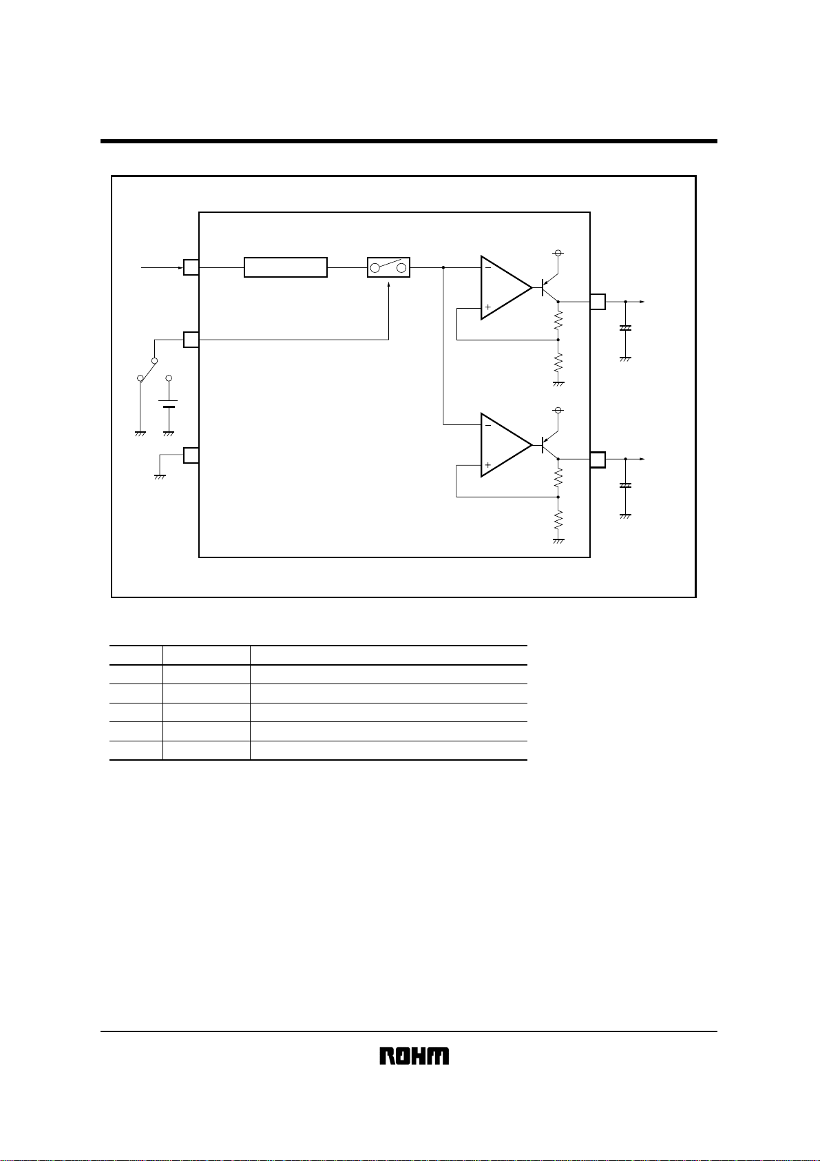
!!!!
Block diagram
V
CC
2
CTL
5
REFERENCE VOLTAGE
BA51W12SAT
9V
1
OUT1
+
GND
3
!!!!Pin descriptions
Pin No.
1
2
3
4
5
Pin name
OUT1
GND
OUT2
V
CC
CTL
Output1 (9V, 1A)
Power supply
Ground
Output2 (5V, 500mA)
ON / OFF switch
Function
5V
4
OUT2
+
Page 3
Regulator ICs
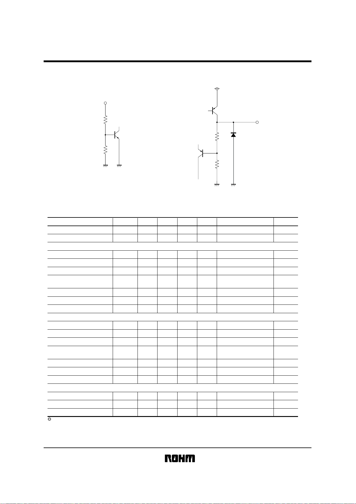
!!!!Input / output circuits
CTL (5pin)
OUT1, 2
CC (2pin)
V
BA51W12SAT
25k
25k
GND (3pin)
12.4k (1pin)
6k (4pin)
2k
GND (3pin)
1, 4pin
!!!!Electrical characteristics (unless otherwise noted, Ta=25°C, VCC=14.0V)
Conditions Test circuit
OFF mode
ON mode
I
O1
=500mA
I
O1
=500mA VCC=8.55V
O1
=500mA, f=120Hz
I
IN
=1V
rms
e
VCC=10→25V, IO=500mA
I
O
=5mA→1A
CC
=25V
V
O2
=350mA
I
I
O2
=350mA VCC=4.75V
O2
=350mA, f=120Hz
I
IN
=1V
rms
e
VCC=6→25V, IO=350mA
I
O
=5mA→500mA
V
CC
=25V
Output ACTIVE mode
Output OFF mode
th
=5V
V
Fig.4
Fig.4
Fig.1
Fig.3
Fig.1
Fig.2
Fig.1
Fig.1
Fig.5
Fig.1
Fig.3
Fig.1
Fig.2
Fig.1
Fig.1
Fig.5
Fig.6
Fig.6
Fig.7
0
Max. Unit
10 µA
5.0 mA
Parameter
Power save supply current
Bias current
Symbol
I
ST
I
b
Min.
-
-
Typ.
3.0
<9V output section> (Output 1)
Output voltage 1
Minimum I / O voltage differential 1
Output current capacity 1
Ripple rejection ratio 1
Input stabillty 1
Load regulation 1
Output short-circuit current 1
V
O1
∆V
O1
I
O1
R.R1
Reg.I1
Reg.L1
I
OS1
8.55
-
1.0
-
-
-
-
9.0
0.3
55
50
100
150
-
9.45 V
0.5 V
-A
-dB
100 mV
150 mV
-mA
<5V output section> (Output 2)
Output voltage 2
Minimum I / O voltage differential
2
Output current capacity 2
Ripple rejection ratio 2
Input stabillty 2
Load regulation 2
Output short-circuit current 2
V
O2
∆V
O2
I
O2
R.R2
Reg.I2
Reg.L2
I
OS2
4.75
-
500
-
-
-
-
5.0
0.3
60
50
50
100
-
5.25 V
0.5 V
-mA
-dB
100 mV
100 mV
-mA
<Switch section>
ON mode voltage
OFF mode voltage
Input high level current
Not designed for radiation resistance.
Note) All the characteristic values are measured with a 0.33µF-capacitor connected the input pin and 22µF-capacitor connected to the output pin.
Measurements are made by using a plus (tw≤10ms, duty cycle≤5%) in all cases but noise voltage and the ripple rejection ratio.
V
th
V
th
I
IN
2.0
1
2
-
-
-
-
150
-V
0.8 V
- µA
Page 4

Regulator ICs
!!!!Measurement circuits
V
CC
0.33µ
V
CC
CTL GND
5V
OUT1
OUT2
BA51W12SAT
+
22µ
V
+
22µ
V
IO2
I
O1
V
CC
10Ω5W
VCC=1
4V,
VCC=
14V,
VCC=
10→25V,
VCC=6
→25V,
VCC=
14V,
VCC=
14V,
VCC=
14V
VCC=
14V
IO1=
500mA
IO2=
350mA
IO1=
500mA
IO2=
350mA
IO1=
5mA→1A
IO2=
5mA→500mA
when measuring output voltage 1
when measuring output voltage 2
when measuring input stability 1
when measuring input stability 2
when measuring load reguration 1
when measuring load reguration 2
when measuring output current capacity 1
when measuring output current capacity 2
Fig.1 Circuit for measuring output voltage, input stability, load regulation, and output current capacity
OUT1
OUT2
+
22
µ
IO1=
500mA when meauring the ripple rejection ratio 1
IO2=
350mA when meauring the ripple rejection ratio 2
+
22
µ
υ
υ
350mA
+
100µ
IN
e
f=120Hz
0.33µ
=1V
rms
V
CC
CTL GND
VCC=
14V,
VCC=
14V,
5V
500mA
Fig.2 Circuit for measuring ripple rejection ratio
Page 5

Regulator ICs
BA51W12SAT
V
V
V
CC
V
CC
0.33µ
5V
VCC=8.55V when measuring
VCC=4.75V when measuring minimum I / O voltage difference 2
OUT1
OUT2
GNDCTL
+
22µ
V
350mA
minimum I / O voltage difference 1
22µ
+
V
500mA
Fig.3 Circuit for measuring minimum I / O voltage difference
CC
A
V
0.33µ
CC
V
OUT1
OUT2
GNDCTL
+
22µ
+
22µ
5V
VCC=14V, IO=0mA, V
VCC=14V, IO=0mA, V
CTL
=5V when measuring bias current
CTL
=0V when measuring power save current
Fig.4 Circuit for measuring bias current power supply current
OUT1
CC
V
OUT2
GNDCTL
+
V
CC
=25V
0.33µ
+
5V
22µ
A
22µ
A
Fig.5 Circuit for measuring output short-circuit current
Page 6

Regulator ICs
BA51W12SAT
VCC=
14V
OUT1
OUT2
GNDCTL
+
22µ
+
22µ
VV
0.33µ
V
CC
2.0V 0.8V
Fig.6 Circuit for measuring mode switching voltage
V
CC
V
CC
=
14V
0.33µ
A
OUT1
OUT2
GNDCTL
+
22µ
+
22µ
!!!!Application circuit
0.33µ
5V
Fig.7 Circuit for measuring input high level current
OUTPUT1
Vcc
OUTPUT2
CTL
GND
5V
+
22µ
+
22µ
Fig.8
Page 7

BA51W12SAT
Regulator ICs
!!!!Operation notes
(1) Although the circuit examples included in this hand-book are highly recommendable for general use, you should be
thoroughly familiar with circuit characteristics as they relate to your own use conditions. If you intend to change the
number of external circuits, leave an ample margin, taking into account discrepancies in both static and dynamic
characteristics of external parts and Rohm ICs. In addition, please be advised that Rohm cannot provide complete
assurance regarding patent rights.
(2) Operating power supply voltage
When operating within the proper ranges of power supply voltage and ambient temperature, most circuit functions
are guaranteed. Although the rated values of electrical characteristics cannot be absolutely guaranteed,
characteristic values do not change drastically within the proper rages.
(3) Power dissipation (Pd)
Refer to the power dissipation characteristics in Fig.12. If power dissipation exceeds the allowable limit, the
functionality of the IC will be degraded (such as reduction of current capacity by increased chip temperature). Make
sure to use the IC within the allowable range of power dissipation with a sufficient margin.
(4) Preventing oscillation at each output and bypass capacitor
To stop output oscillation, make sure to connect a capacitor between GND and each output pin (capacitance of at
least 10µF over the whole operating temperature range is recommended). Oscillation can occur if capacitance
is susceptible to temperature. We recommended using a tantalum capacitor with minimal changes in capacitance.
Also, output can be further stabilized by connecting a bypass capacitor of about 0.33µF between the input pin and
GND. Place the capacitor as near as possible to the input pin.
(5) Overcurrent protection circuit
An overcurrent protection circuit is installed in each output system, based on the respective output current. This
prevents IC destruction due to overcurrent, by limiting the current with a curve shape of “7” in the voltage current graph. The IC is designed with margins so that current flow will be restricted and latching will be prevented
even if a large current suddenly flows through a large capacitor. Note that these protection circuits are only good for
preventing damage from sudden accidents. Make sure your design does not cause the protection circuit to operate
continuously under transitional conditions (for instance, if output is clamped at 1V
operates at 1V
or lower). Note that the circuit ability is negatively correlated with temperature.
F
or higher, short mode circuit
F
(6) Thermal protection circuit
A built-in thermal protection circuit prevents thermal damage to the IC. All outputs are turned off when the circuit
operates, and revert to the original state when the temperature drops to a certain level.
(7) We recommend installing a bypass line with a diode in your application if there is a mode where potential difference
between each output and input (V
) or GND is reversed from the normal state. A reversed mode may cause
CC
damage to the IC.
(8) Although the quality of this IC is rigorously controlled, the IC may be destroyed when the applied voltage or the
operating temperature exceeds their absolute maximum ratings. Because short mode or open mode cannot be
specified when the IC is destroyed, be sure to take physical safety measures, such as fusing, if any of the absolute
maximum ratings might be exceeded.
Page 8

BA51W12SAT
Regulator ICs
(9) Recommended to put diode for protection in case of output pin connected with large load of impedance or reserve
current occurred at initial and output off.
(Example)
Output
(10) When used within a strong magnetic field, be aware that there is a slight possibility of malfunction.
(11) We are confident in recommending the above application circuit example, but we ask that you carefully check the
characteristics of this circuit before using it. If using circuit after modifying other external circuit constants, be careful to
ensure adequate margins for variation between external devices and this IC, including not only static characteristics
but also transient characteristics.
This IC is a bipolar IC which (as shown in Figure 9) has P+ isolation in the P substrate and between the various pins.
A P-N junction is formed form this P layer and the N layer of each pin. For example the relation between each
potentials is as follows,
(When GND > PinB and GND > PinA, the P-N junction operates as a parasitic diode.)
(When PinB > GND > PinA, the P-N junction operates as a parasitic transistor.)
Parasitic diodes can occur inevitably in the structure of the IC. The operation of parasitic diodes can result in mutual
interference among circuits as well as operation faults and physical damage. Accordingly, you must not use methods
by which parasitic diodes operate, such as applying a voltage that is lower than the GND (P substrate) voltage to an
input pin.
(Pin A)
Resistance
(Pin B)
C
Transistor (NPN)
B
E
GND
N
P
N
P substrate
GND
B
GND
C
E
+
P
N
Parasitic diode
or transistor
+
P
N
P substrate
(Pin A)
N
GND
P
Parasitic diode
GND
Parasitic diode
+
P
N
Fig.9 Simplified structure of bipolar IC
+
P
N
Parasitic diode or
transistor
(Pin B)
Page 9

Regulator ICs
!!!!Electrical characteristic curves
12
11
10
V)
(
9
O
8
V
O1
7
6
5
V
O2
4
3
OUTPUT VOLTAGE : V
2
1
0
0 500 1000 1500 2000
OUTPUT CURRENT : I
Fig.10 Output current capacity
characteristics (Typ.)
!!!!External dimentions (Units : mm)
O
(
mA)
VCC=14V
Ta=25˚C
10
9
8
V)
(
O
7
6
5
4
3
OUTPUT VOLTAGE : V
2
1
0
0 6 12 2418 3630 42 54 6048
POWER SUPPLY VOLTAGE : V
Fig.11 Output voltage
characteristics (Typ.)
Ta=25°C
O
=0mA
I
V
O1
V
O2
Over voltage
protection circuit,
ON Vcc=28V(Typ .)
CC
(
V)
BA51W12SAT
28
24
20
16
12
8
POWER DISSIPATION : Pd (W)
4
0
0 25 50 10075 125 150
AMBIENT TEMPERATURE : Ta (˚C)
Fig.12 Thermal derating characteristics
(1) With infinte heat sink
(2) With Al heat sink
100×100×2 (mm
(3) With Al heat sink
50×50×2 (mm
(4) Without heat sink
Note : When using AI
heat sink, a tightening
torque of 6 (kg cm) and
silicon grease is applied
(2)
(3)
(4)
2
)
2
)
3.2 ± 0.1
φ
0.5 + 0.1
+ 0.3
4.5
− 0.1
+ 0.2
2.8
− 0.1
2.85
+ 0.4
31.5Max.
17.0
− 0.2
12.0 ± 0.2
1.8 ± 0.2
8.0 ± 0.2
+ 0.4
− 0.2
17.0
13.5Min.
12.0 ± 0.2
1.8 ± 0.2
8.0 ± 0.2
1.2 ± 0.2
+ 0.3
10.0
− 0.1
+ 0.3
7.0
− 0.1
0.7
1.2
0.8
23451
1.778
TO220FP-5 TO220FP-5(V5)
+ 0.3
10.0
− 0.1
+ 0.3
7.0
− 0.1
12345
+ 0.3
4.5
− 0.1
+ 0.2
0.5 ± 0.1
2.8
− 0.1
17.5
(2.0)
25.8
23.4
(2.85)
4.25
8.15
3.2 ± 0.1
φ
1.2
0.8
1.778
 Loading...