

Page 1
Audio ICs
1.5V / 15mW dual power amplifier
BA5152F
The BA5152F is a dual-channel power amplifier designed for 1.5V headphone stereos. The circuit consists of a power
supply circuit, mute circuit, bias circuit, and two amplifier circuits. T o simplify assembly, the gain is fixed, so external ne gative-feedback components are not required.
Applications
1.5V headphone Hi-Fi stereos
Features
1) High output. P
2) Small “pop” noise.
3) Mute circuit terminal provided.
4) T erminals provided for radiation countermeasures.
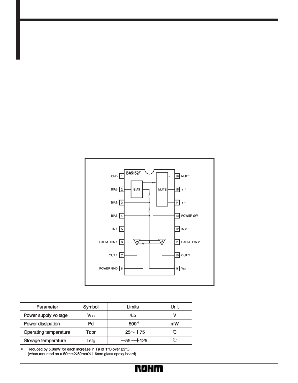
Block diagram
OUT = 15mW (RL = 16Ω).
5) Good ripple rejection ratio.
6) Few external components required.
7) Good low-voltage characteristics.
8) Built-in power switch circuit.
Absolute maximum ratings (Ta = 25C)
367
Page 2
Audio ICs BA5152F
Recommended operating conditions (Ta = 25C)
Electrical characteristics (unless otherwise noted, Ta = 25C, V
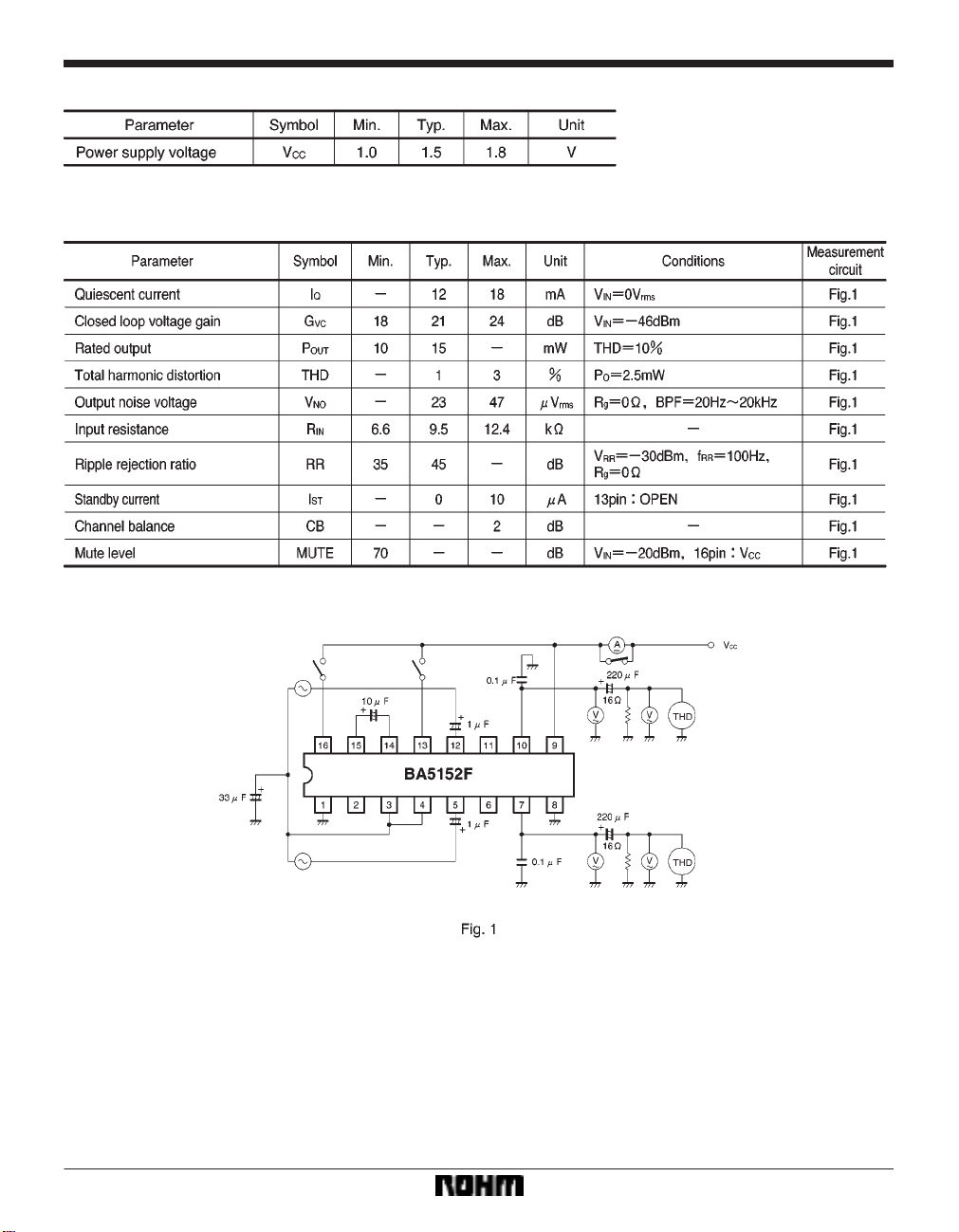
Measurement circuit
CC = 1.5V, f= 1kHz and RL = 16Ω)
368
Page 3

Audio ICs BA5152F
Application example
Application board patterns Application board component layout
369
Page 4

Audio ICs BA5152F
Complete application example circuit
Circuit description
(1) Power supply block
The BA5152F has an internal power switch, so the V
terminal (pin 9) connects directly to the power source. Pin
13 is the power switch, and if it is left open, no bias current
flows in the circuit and the IC will not operate.
(2) Mute circuit block
CC
When pin 13 is connected to V
CC, the IC starts up, but the
mute circuit operates to suppress a “pop” sound from being generated. The time constant of the power-on mute
circuit is determined by the capacitor connected between
pins 14 and 15. It is also possible to force the mute circuit
to operate by connecting pin 16 to V
CC. There is no time
constant in this case.
370
Page 5

Audio ICs BA5152F
(3) Bias block
The components connected to pins 2, 3, and 4 set the
bias point and V
ODC. When pin 2 is open circuit, and VCC
= 1.25V, the output pin VODC voltage is internally set to
1/2V
CC. By connecting a resistor to pin 2 and changing
the voltage divider ratio, it is possible to vary V
ODC.
Pins 3 and 4 are shorted and connected to earth via an
electrolytic capacitor to generate the bias point. When a
33µF component is used, it is possible to obtain 45dB of
ripple rejection. This can be improved if pins are independently grounded through capacitors.
Electrical characteristics curves (Ta = 25C)
(4) Amplifier block
The amplifier circuits have a fixed gain of G
V = 21dB. The
negative-feedback circuits are on the chip, and the
ground point of the negative-feedback circuit uses the
bias point as its reference, so connect the input potentiometer to the bias point pins (3 and 4). Connect bypass
capacitors to the output pin to prevent oscillation. When
the IC is used in sets containing an AM radio, it is possible
to reduce unnecessary radiation from the power amplifiers by connecting CR circuits to pins 6 and 11.
371
Page 6

Audio ICs BA5152F
External dimensions (Units: mm)
372
 Loading...