

Page 1
Regulator ICs
System power supply for car stereos
BA3918
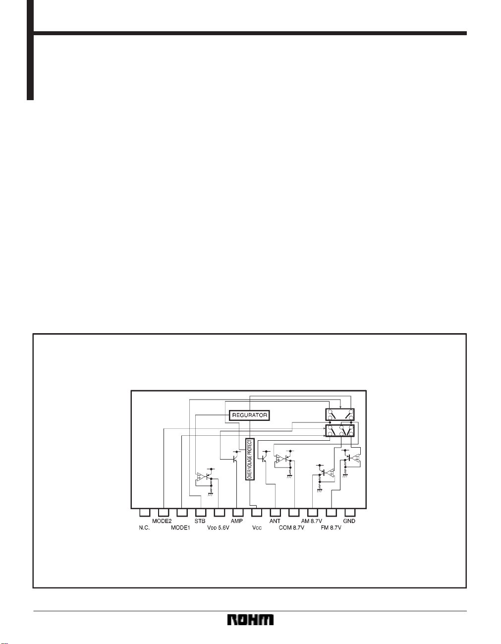
The BA3918 is a single-chip power supply IC for use in car audio systems. One 5.6V output for a microcontroller, three
8.7V outputs, and two outputs interlocked by BACKUP and ACC systems are built in.
Applications
Car audio systems
Features
1) All outputs except AMP and ANT use a PNP transistor with a low saturation voltage.
2) Output current limit circuit prevents damage to the IC
due to short-circuiting.
3) Overvoltage protection circuit provides protection
against surges from the A
CC or BACKUP input.
4) Compact 12-pin POWER package allows large power dissipation.
5) Thermal protection circuit prevents heat damage to
the IC.
Block diagram
242
Page 2
Regulator ICs BA3918
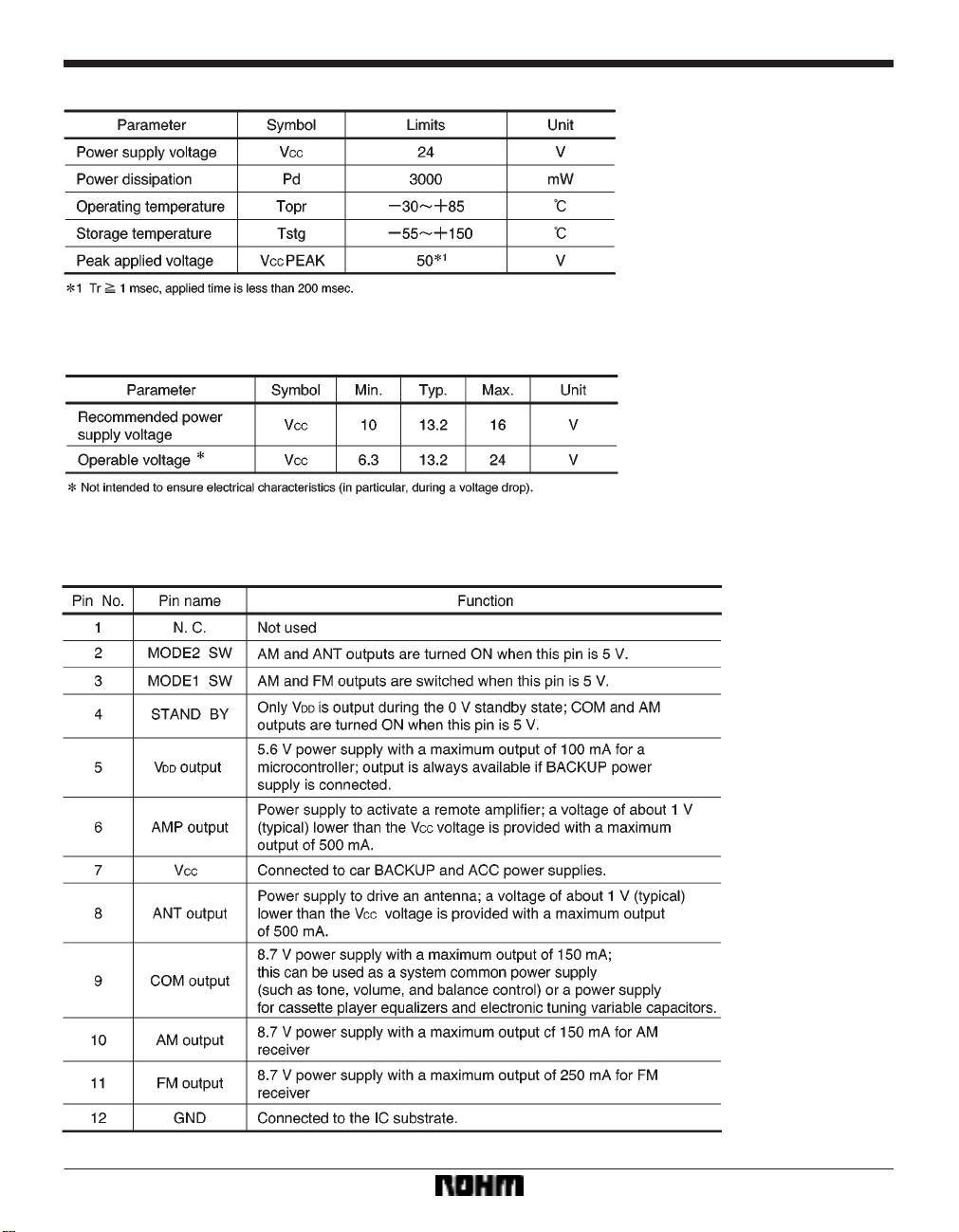
FAbsolute maximum ratings (Ta = 25_C)
FRecommended operating conditions (Ta = 25_C)
FPin descriptions
243
Page 3
Regulator ICs BA3918
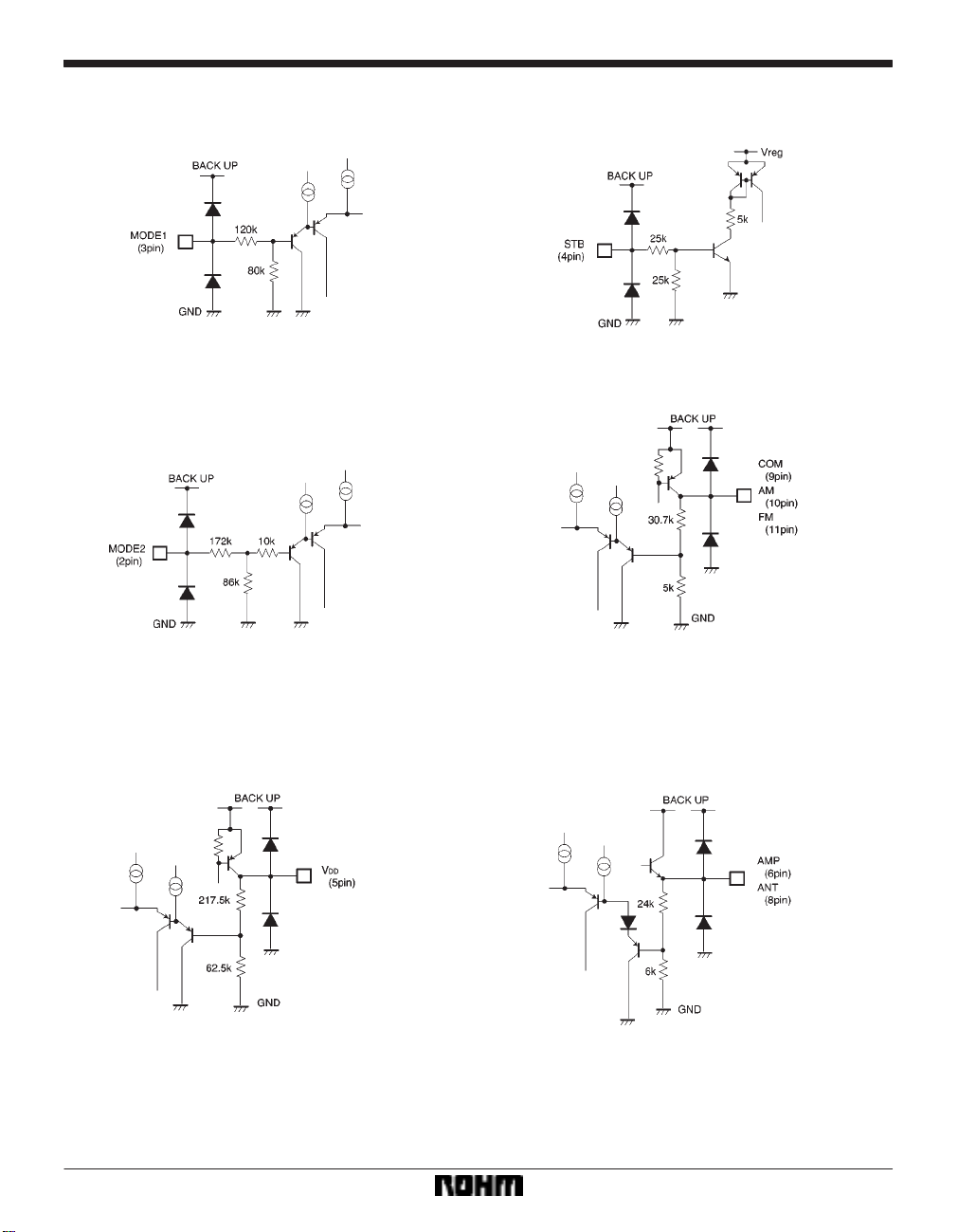
Input / output circuits
244
Page 4

Regulator ICs BA3918
FElectrical characteristics (unless otherwise noted, Ta = 25_C and VCC = 13.2V)
245
Page 5

Regulator ICs BA3918
Input / output timing chart
246
Page 6

Regulator ICs BA3918
FEstimate of allowable power dissipation
Except under transitional conditions, the power dissipation of this IC is 3W per unit at 25_C.
See Fig. 4 for thermal derating characteristics, including some cases where heat sinks are used.
S Power consumed by V
DD 5.6V P1 = (A 5.6V) I1 (I1 / 20 I1 / 10) A
S Power consumed by COM 8.7V P
S Power consumed by AMP P
S Power consumed by ANT P
S Power consumed by AM 8.7V P
S Power consumed by FM 8.7V P
S Power consumed internally by each circuit P
P
Max. = P1 P2 P3 P4 (P5 or P6, whichever is greater) P7
A = maximum voltage for V
CC
I1 = maximum output current for VDD
I2 = maximum output current for COM
I
3 = maximum output current for AMP
4 = maximum output current for ANT
I
5 = maximum output current for AM
I
6 = maximum output current for FM
I
2 = (A 8.7V) I2 (I2 / 30 I2 / 10) A
3 = 1V I3 (22mA) A
4 = 1V I4 (22mA) A
5 = (A 8.7V) I5 (I5 / 30 I5 / 10) A
6 = (A 8.7V) I6 (I2 / 50 I6 / 10) A
7 = VCC circuit current (about 5mA)
247
Page 7

Regulator ICs BA3918
Application example
248
Page 8

Regulator ICs BA3918
Operation notes
(1) Example of application
The application circuit of Fig. 3 is recommended for use.
Make sure to confirm the adequacy of parts characteristics. When using the circuit with changes to external circuit constants, make sure to leave sufficient margins in
consideration of fluctuations in the IC and external components including static and transitional characteristics.
Note that ROHM has not carried out extensive survey regarding the patent right of this application.
(2) Operating power supply voltage
When operating within the proper ranges of power supply
voltage and ambient temperature, most circuit functions
are guaranteed. Although the rated values of electrical
characteristics cannot be absolutely guaranteed, characteristic values do not change drastically within the
proper ranges.
(3) Power dissipation (Pd)
Refer to the power dissipation curves (Fig. 4) and the
rough estimation of IC power dissipation given on a separate page. Make sure your design allows a maximum
power within the operating temperature range.
(4) Overvoltage protection circuit
The overvoltage protection circuit turns OFF all outputs
when the potential difference between V
CC (pin 7) and
GND (pin 12) is more than about 26V at normal temperature. Make sure to use the IC within this voltage limit.
(5) Preventing oscillation at each output
T o stop output oscillation, make sure to connect a capacitor having a capacitance of 10µF or greater between
GND and each of the V
DD (pin 5), COM (pin 9), AM (pin
10), and FM (pin 11) output pins. We recommend using
a tantalum electrolytic capacitor whose capacitance is
unsusceptible to temperature.
(6) Overcurrent protection circuit
An overcurrent protection circuit is installed on the V
(pin 5), AMP (pin 6), ANT (pin 8), COM (pin 9), AM (pin
10), and FM (pin 11) outputs, based on the respective
output current. This prevents IC destruction due to overcurrent, by limiting the current with a curve shape of “7”
in the voltage-current graph. The IC is designed with
margins so that current flow will be restricted and latching
will be prevented even if a large current suddenly flows
through a large capacitor. The circuit should be carefully
set because output current is further restricted when output voltage is less than 1V
F (considered as short mode).
(7) Thermal protection circuit
A built-in thermal protection circuit prevents thermal
damage to the IC. All outputs except V
OFF when the circuit operates, and revert to the original
state when temperature drops to a certain level.
(8) Grounding
Each ground trace in the application circuit of Fig. 3 must
be adequately short from GND (pin 12). Make sure to arrange the ground traces in a pattern that prevents mutual
interference.
(9) Although the quality of this IC is rigorously controlled, the IC may be destroyed when the supply voltage
or the operating temperature exceeds their absolute
maximum ratings. Because short mode or open mode
cannot be specified when the IC is destroyed, be sure to
take physical safety measures, such as fusing, if any of
the absolute maximum ratings might be exceeded.
(10) We recommend installing a bypass line in your application if there is a mode where potential difference between each output and input (V
CC) or GND is reversed
from the normal state.
Thermal derating characteristic curve
DD
DD are switched
249
Page 9

Regulator ICs BA3918
Electrical characteristic curves
External dimensions (Units: mm)
250
 Loading...