

Page 1
1
Standard ICs
EL driver for portable sets
BA3899F
The BA3899F is an IC developed for EL drive applications. It uses a more compact interface than transformer systems, and is ideal for use in thin sets.
•
Applications
Pagers, electronic notebooks and other portable devices
•
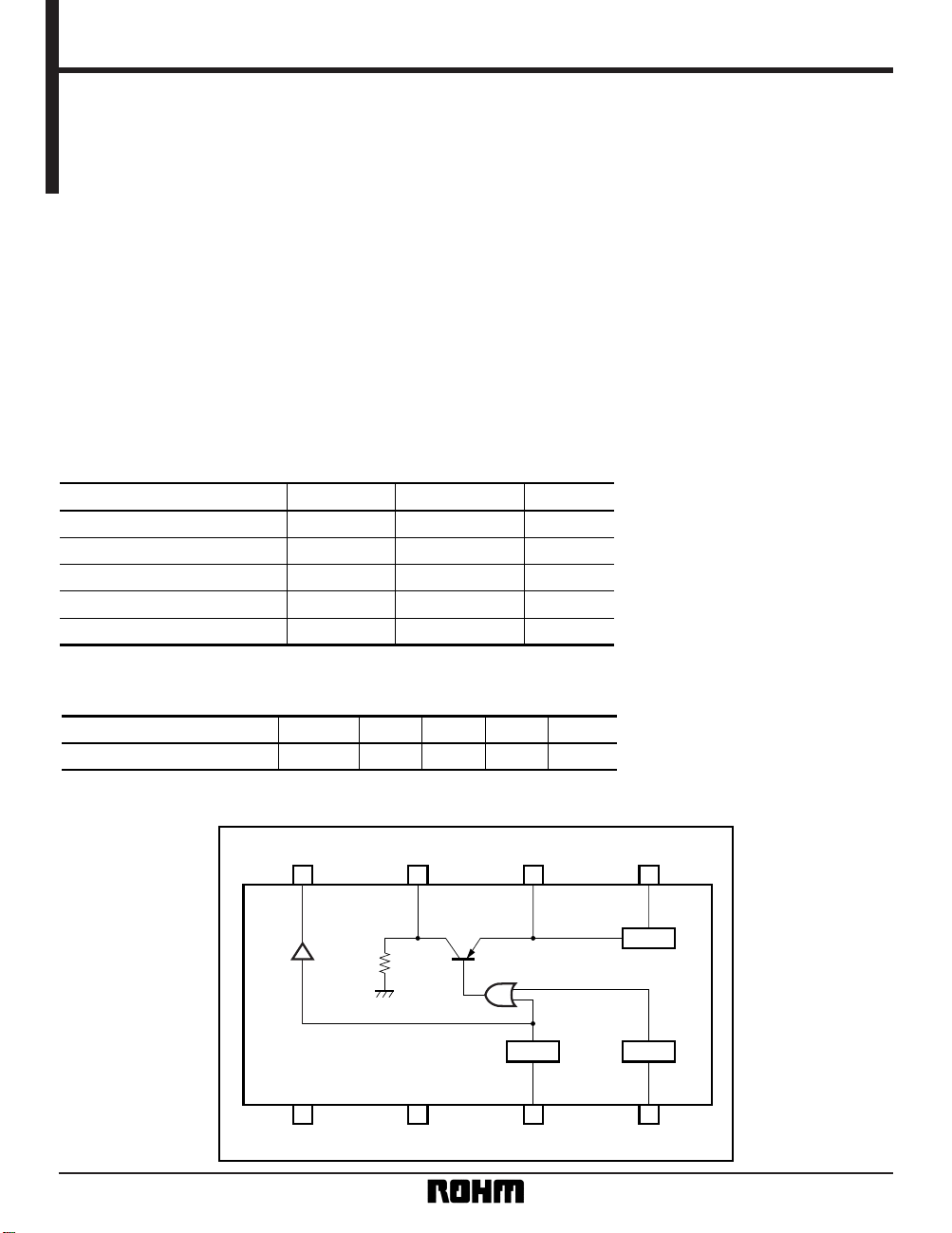
Block diagram
8
7
6
1 2
3
5
STBY
4
GND
N.C. C1
C2
SW1 SW2 V
CC STBY
OSC2
OSC1
R
SW2
•
Features
1) Drive oscillation frequency can be set using external capacitance.
2) Equipped with standby control pin.
•
Absolute maximum ratings (Ta = 25°C)
Parameter
Power supply voltage
Power dissipation
Operating temperature
Storage temperature
V
CC
Pd
Topr
Tstg
8.0
450
∗
– 10 ~ + 60
– 55 ~ + 125
V
Symbol Limits Unit
mW
°C
°C
Maximum applied voltage VST 8.0 V
∗
Reduced by 4.5mW for each increase in Ta of 1°C over 25°C.
•
Recommended operating conditions (Ta = 25°C)
Parameter
V
CC 1.0 5.0 7.0 V
Symbol Min. Typ. Max. Unit
Power supply voltage
Page 2
2
Standard ICs BA3899F
•
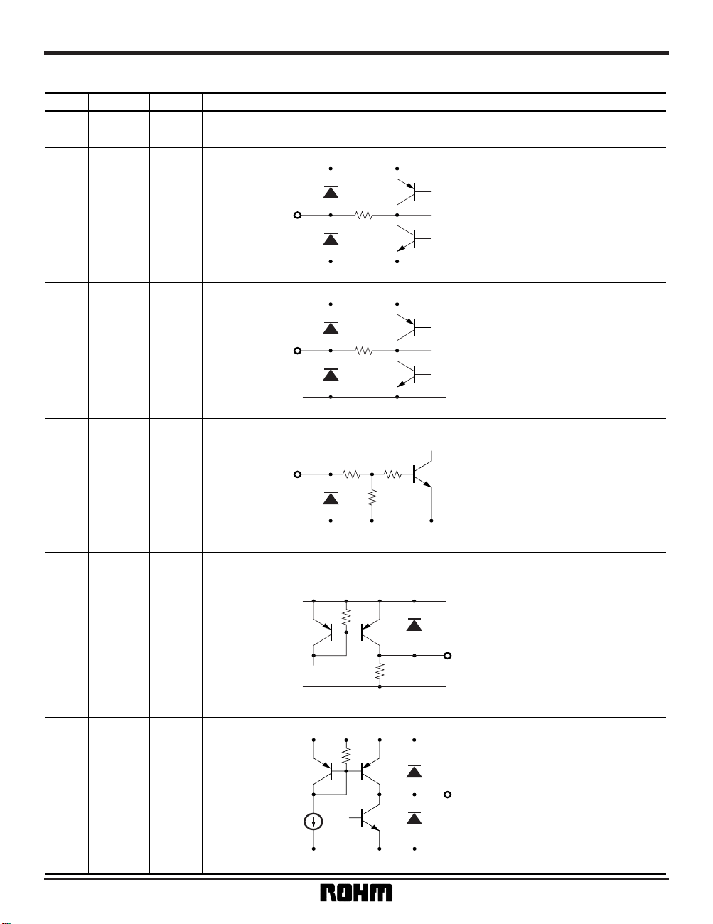
Pin descriptions
V
CC
GND
C1
1k
V
CC
GND
C2
200Ω
V
CC
GND
SW2
50k
500Ω
X20X1
GND
STBY
1k
200k
50k
V
CC
GND
SW1
X5X1
Pin No.
OSC1 oscillator circuit;
external capacitor pin
OSC2 oscillator circuit;
external capacitor pin
Standby control pin
(HIGH state: standby cancelled)
SW2 switching output pin
SW1 switching output pin
䊊When applying resistance, etc.
to the STBY pin, be careful not
to exceed the threshold values.
—
—
2——N.C.
—V
CC
input pin
6I—V
CC
3 I / O —C1
4 I / O —C2
5I0STBY
7O—SW2
8O—SW1
1 I — — GND pinGND
Pin name I / O Pin voltage Internal equivalent circuit Function
Page 3
3
Standard ICs BA3899F
•
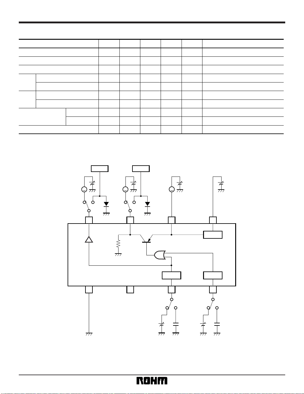
Electrical characteristics (unless otherwise noted, Ta = 25°C, VCC = 5.0V, C1 = 0.033µF, C2 = 1500pF)
Parameter
Symbol Min. Typ.
Supply current ICC mA When used as stand-alone unit3.0 4.6 6.2
C1 pin oscillation frequency fSW1 Hz75 95 120
C2 pin oscillation frequency fSW2 kHz17 23 29
Source current
SW1
SW2
Standby pin control
voltage condition
ISW1SO µAVC1 = 1.0V, VC2 = 0.05V, VSW1 = 0V100 140 180
Sink current ISW1SI µAVC1 = 0.05V, VC2 = 0.05V, VSW1 = 1.0V– 40 — —
Source current ISW2SO mA VC1 = 0.05V, VC2 = 0.05V, VSW2 = 0V3.2 4.4 6.1
Pull-down resistance RSW2 Ω Vst = 0.35V, VSW2 = 0.3V400 500 600
Operating VSTON V1.0 — — —
—
—
—
—
Non-operating VSTOFF V— — 0.3
Quiescent current in standby state IQ (ST) µA— 0 2.0
Max. Unit Conditions
•
Measurement circuit
2
ISW1
VSW1
fSW1
VCC
Counter
VC1
0.033µF
IQ
VSTBY
8
VC2
1500pF
± 1%
± 1%
1
ISW2
VSW2
fSW2
Counter
7
3 4
STBY
OSC2
OSC1
R
SW2
Fig.1
A A
A
6 5
Page 4

4
Standard ICs BA3899F
•
Application example
567
STBY
8
OSC2
OSC1
Fig. 2
RSW2
EL 16000pF R1 2k
D1
Q2
Q1
L1
100k
V
CC = 5V
ROHM: 1SS376
ROHM: 2SC4061KP
SW1 SW2 STBY
R
X
300k
V
CC
SANYO: 2SC3645T
1.5mH (TOKO: D73LC)
∗
GND N.C. C1
C1
8200pF ± 10%
2.2µF
C2
1500pF ± 10%
C2
1234
+
∗
Because of the characteristics of the EL element, continuous application of particularly high DC power supply voltage can shorten the lifetime of the
element. To avoid this, we recommend inserting a switch in the power supply line.
Page 5

5
Standard ICs BA3899F
2
5
STBY
GND N.C. C1 C2
SW1
R1 4.7k
ROHM: 1SS376
D1
EL 5000pF
SW2 V
CC
VCC = 1.5V
STBY
OSC2
OSC1
R
SW2
Q1
Q2
L1
1mH
ROHM: 2SC4061KP
SANYO: 2SC3143K5
(
TOKO: 43FS) or (TDK: NL453232
)
C2
1500pF ± 10%
C1
0.033µF ± 10%
41 3
68 7
VSTBY = 1.5V
Hi: act
Fig. 3
2.2µF
+
Page 6

6
Standard ICs BA3899F
•
Operation notes
(1) EL drive output
As shown in Figure 4, the EL drive output consists of
charging (rise in voltage caused by switching) and discharging waveforms. The switching frequency is determined by f
SW2 and the charging and discharging timing
by f
SW1.
(4) Q1, Q2, and D1
The V
O (Max.) shown in Figure 4 is applied to the output
V
O, so if using any transistor other than that recom-
mended, caution is required concerning the pressure
withstand value. Also, Q2 must have characteristics
which allow it to keep pace with the switching speed of
f
SW2.
t1
tSW1 (fSW1)
V
O (Max.)
t2
Charge
Discharge
Fig.4
(2) Setting fSW1
The oscillation frequency is determined by charging
and discharging of the external capacitance of the C1
pin. The value for C1 should be set based on the following equation.
(5) R
X (resistor for adjusting light volume)
With a configuration like that shown in Figure 5, the
volume of light can be adjusted. However, R
X should
be set so that I
X satisfies the following condition.
C1 = ×
= (3.14E – 6) ×
( + ) V
C1 ×
(V
CC = 5V)
1
11
I
1
1
f
SW1
I2
1
fSW1
Ix ( = ) < 40µA
Vx – 0.2V
Rx
If IX > 40µA, LSI dispersion, temperature fluctuation,
and other elements can cause oscillation of the C2 pin
to stop. Be sure the above condition is satisfied.
The recommended setting range for f
SW1 is 40Hz to
800Hz. However, the V
O (Max.) shown in Figure 4 is
determined by f
SW1, so caution is required concerning
the pressure withstand values of Q1, Q2, and D1.
(3) f
SW2
fSW2 is the switching pressure rise frequency, and is
determined by the external capacitance of the C2 pin.
This value (1500pF) is determined by the inductance
value and the Q2 transistor capability. When changing
this value, the drive capability of Q2 must be taken into
consideration in order to avoid the possibility of malfunction.
4
C2
1500pF
Vx
Rx
Ix
Fig.5
Page 7

7
Standard ICs BA3899F
•
Electrical characteristic curves
0
012345678910
1
2
3
4
5
6
7
C1 = 0.033µF
C2 = 1500pF
V
ST = 5V
Rx = ∞
8
9
10
QUIESCENT CURRENT: ICC (mA)
75°C
– 25°C
25°C
INPUT VOLTAGE: V
CC (V)
Fig. 6 Supply current (when used
as stand-alone unit) vs.
power supply voltage
10k
1k
100
023154678
OSCILLATION FREQUENCY: fSW (Hz)
C1 = 0.033µF
C2 = 1500pF
Rx = ∞
75°C
fSW1
fSW2
– 25°C
25°C
75°C
– 25°C
25°C
INPUT VOLTAGE: VCC (V)
Fig. 7 Oscillation frequency of C1
and C2 pins vs. power supply
voltage
SW1 SOURCE CURRENT: ISWISO (µA)
0
012345678910
50
100
150
200
250
VC1 = 1.0V
V
SW1 = 0V
25°C
– 25°C
75°C
INPUT VOLTAGE: V
CC (V)
Fig. 8 SW1 sink current vs.
power supply voltage
SW1 SINK CURRENT: ISW1SI (%)
INPUT VOLTAGE: VCC (V)
0
012345678910
10
2.0
3.0
1.0
VC1 = 0V
V
SW1 = 1.0V
V
ST = 5V
25°C
– 25°C
75°C
Fig. 9 SW1 source current vs.
power supply voltage
0
012345678910
1
2
3
4
5
6
7
V
C1 = 1.0V
V
SW1 = 0V
V
ST = 5V
8
9
10
SW2 SOURCE CURRENT: ISW2SO (mA)
INPUT VOLTAGE: VCC (V)
75°C
– 25°C
25°C
Fig. 10 SW2 source current vs.
power supply voltage
0
012345678910
100
200
300
400
500
600
700
VCC = 5V
V
SW2 = 0.2V
V
ST = 0V
800
900
1000
SW2 PULL-DOWN RESISTANCE: RSW2 (Ω)
INPUT VOLTAGE: VCC (V)
75°C
– 25°C
25°C
Fig. 11 SW2 pull-down resistance vs.
power supply voltage
Page 8

8
Standard ICs BA3899F
•
External dimensions (Units: mm)
SOP8
0.4 ± 0.11.27
0.15
0.3Min.
0.15 ± 0.1
0.11
6.2 ± 0.3
4.4 ± 0.2
5.0 ± 0.2
85
41
1.5 ± 0.1
 Loading...