

Page 1
Audio ICs
Stereo sound controller IC
BA3853BFS
The BA3853BFS is a dual-channel electronic volume controller built around a low-noise, low-distortion VCA. It is suited
for car-audio applications, and has performance that rivals mechanical-type volume controllers.
In addition to volume control, the IC includes all functions required for controlling sound quality, to allow more compact
designs with far fewer components.
Applications
Car audio systems
Features
1) Provides electronic control for volume, balance, fader, tone (bass and treble), and loudness.
2) The volume control circuit is a low-distortion, lownoise VCA circuit that uses DC voltage for control.
The IC uses an internally-generated, temperaturecompensated reference voltage and is capable of
dual-channel control with the addition of a single potentiometer.
3) Available in an SSOP-24 package that is ideal for
compact designs.
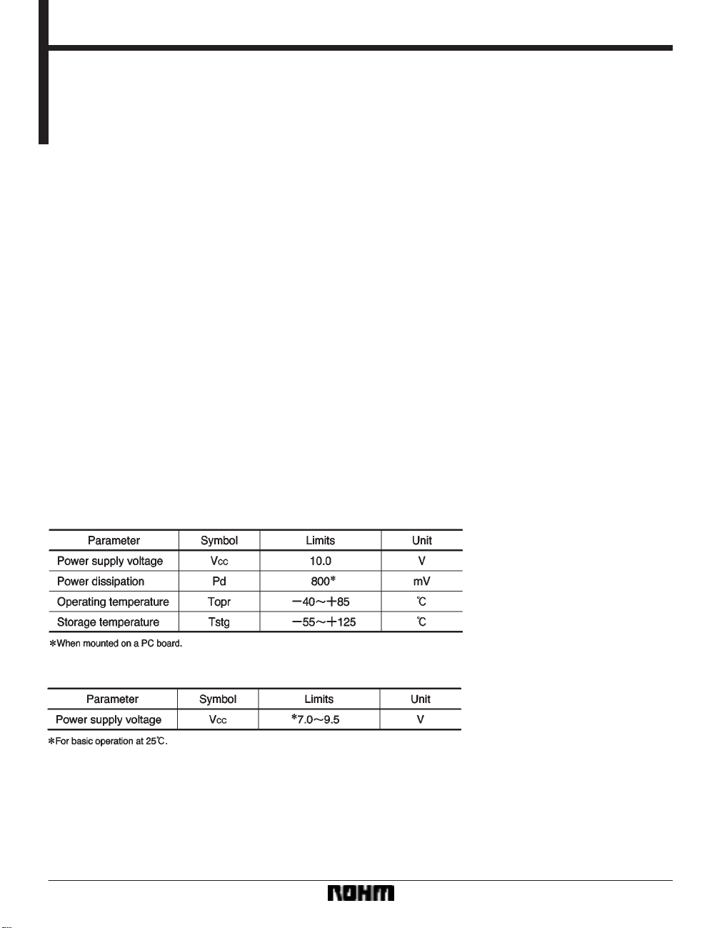
Absolute maximum ratings (Ta = 25C)
Recommended operating conditions (Ta = 25C)
791
Page 2
Audio ICs BA3853BFS
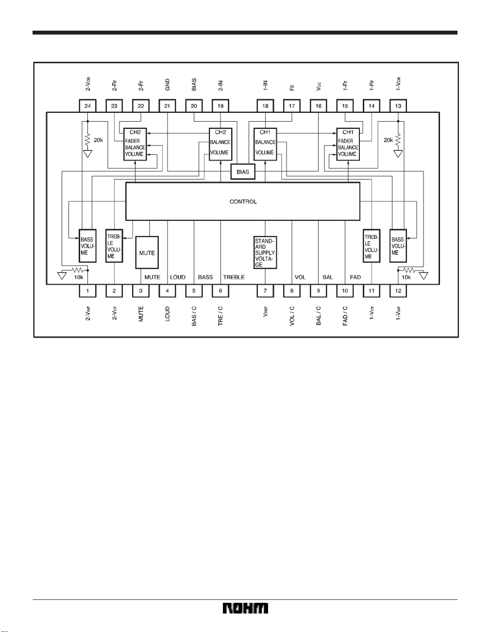
Block diagram
792
Page 3
Audio ICs BA3853BFS
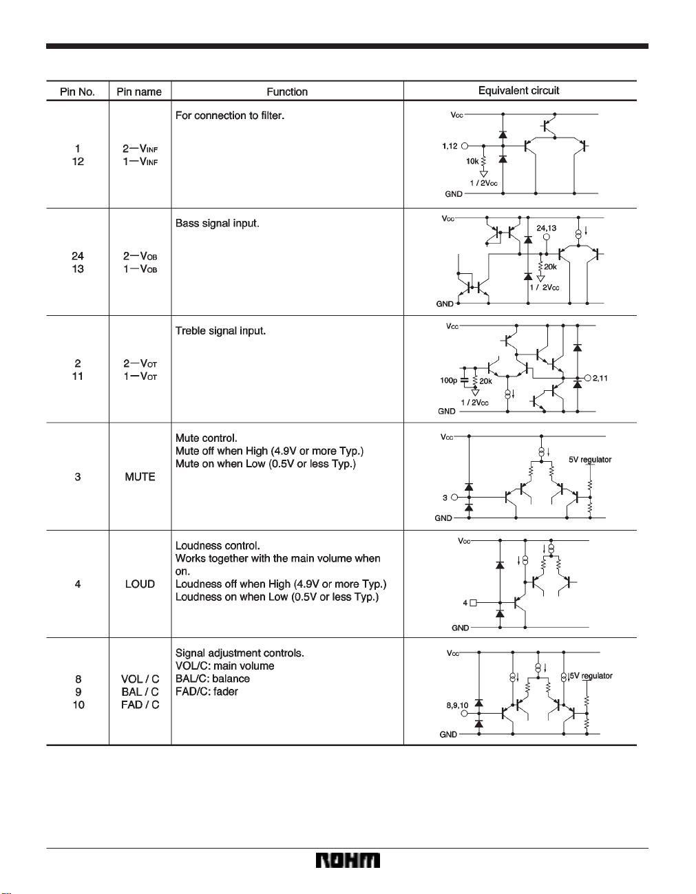
Pin descriptions and input / output circuits
793
Page 4

Audio ICs BA3853BFS
794
Page 5

Audio ICs BA3853BFS
Electrical characteristics (unless otherwise noted, Ta = 25C, VCC = 8V, f = 1kHz, BW = 20Hz to 20kHz,
VOL / C = MAX, TONE = ALL FLAT, FAD / C = FLAT, BAL / C = FLAT, LOUD = OFF, and MUTE = OFF)
Operating specifications
(1) Input and output signals have the same phase.
(2) Maximum loudness control variation occurs at 30dB ATT. At 10dB ATT, the variation is 0dB.
(3) For loudness operation during tone adjustment, arithmetic processing is performed with the maximum tone varia-
tion amount.
795
Page 6

Audio ICs BA3853BFS
Measurement circuit
796
Page 7

Audio ICs BA3853BFS
Measurement circuit switch operation
A, B and C in the table refer to the following:
A: Max. volume
B: 1 / 2 volume
C: Min. volume
797
Page 8

Audio ICs BA3853BFS
Circuit operation
(1) As shown is the block diagram, the main circuit
blocks are the main volume (front and rear), tone control
(bass and treble), and balance and fader. Signal control
for each block is possible with a DC voltage.
(2) The main volume is comprised of a front volume
and rear volume controller. The front volume controller
has 18dB of attenuation.
Application example
(3) The tone filter is an external CR circuit. Refer to item
5 of the application notes regarding the component values.
(4) The loudness is set by a calculation based on the
tone control current. Refer to control curves item 3 of the
application notes.
(5) The control curves for the balance and fader are
given in the measurement data.
798
Page 9

Audio ICs BA3853BFS
External components
(1) Mute and loudness circuit components
Select the values for the mute and loudness on / off pin
components to suit the product that you are designing.
The value of the resistor should be 2.2MΩ or less.
Set the circuit time constant as follows:
(2) External filter circuits
The filter circuits are built using passive components,
and the resistors for both the bass and treble filters are
on the chip. Construct the circuits shown below.
When using a switch as illustrated in the circuit diagram,
set the values for C and R in the time-constant circuit as
follows:
(1) When the switch is on (rise)
V = Vreg EXP (*
CR
t
2
1
/(R1)R2)
)
(2) When the switch is off (fall)
t
V = Vreg (1 * EXP ( *
))
1C2
R
V: pin 3 or pin 4 voltage
Filter cutoff frequencies
The circuits given above have the following frequency
characteristics.
(1) Bass filter cutoff frequency
fc1 =
2πC
1
=
1R1
2πC
1
1 20kΩ
(2) Treble filter cutoff frequency
High-pass filter side
2 =
2πC
1
=
2R2
fc
2πC
1
2 10kΩ
Low-pass filter side
1
3 =
fc
2πC
= = 80kHz
3R3
2πc
1
3 100pF 20kΩ
The tone control circuit is designed to give a change of
±15dB (Typ.) for the frequency that you wish to boost or
cut at the peak and bottom of the frequency characteristic. Design the filter with due consideration to the frequency characteristics. The values for the filter given in
the application circuit have been selected to give sufficient boost and cut at f = 100Hz and f = 10kHz.
799
Page 10

Audio ICs BA3853BFS
Application notes
(1) Power supply voltage range
Operation of the basic functions of the application example circuit are guaranteed if operated within the stipulated
power supply voltage and ambient temperature ranges.
Rohm cannot guarantee the ratings for the electrical
characteristics, but these will not change radically if the
circuit is operated within the stipulated power supply voltage and ambient temperature ranges.
(2) Mute circuits
Both the main volume and fader volume circuits have a
built-in mute circuit. Mute is applied to all output pins.
Mute logic
(3) Loudness control
(1) The loudness circuit is designed to work together
with the main volume.
(2) Maximum loudness change occurs when the signal
attenuation is 30dB or lower. Up to a signal attenuation
of 10dB, the circuit is designed to have a change in
loudness of 0dB.
(3) For signal attenuation between 10dB to 30dB,
the change in loudness is smaller approaching 10dB,
and gets larger approaching 30dB.
(4) When loudness is operated during tone adjustment,
if the amount of boost due to the combined tone boost
and loudness exceeds the maximum boost, the circuit
design ensures that the amount of loudness change will
not exceed the maximum amount of tone boost (see
Figs. 6 and 7).
(5) Loudness is on when the pin voltage is below 2.5V,
and off above 2.5V.
(4) Balance / fader
(1) Balance control curve
The balance control curve has been designed so that at
above 2.8V, channel 1 (1-Fr, 1-Rr) is attenuated, and at
below 2.2V, channel 2 (2-Fr, 2-Rr) is attenuated.
(2) Fader control curve
The fader control curve has been designed so that at below 2.2V , the front (1-Fr, 2-Fr) is attenuated, and at above
2.8V, the rear (1-Rr, 2-Rr) is attenuated.
(5) Input / output circuits
Buffers are used before and after the signal input and
output pins.
800
Page 11

Audio ICs BA3853BFS
External dimensions (Units: mm)
801
 Loading...