

Page 1

Audio ICs
Low-current audio headphone driver
BA3574BFS
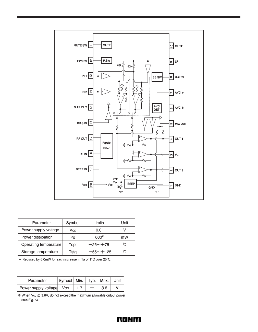
The BA3574BFS is a headphone driver with a fixed-gain bass boost circuit and an AVC circuit that keeps the output
below a fixed level. It features low current dissipation, and low output noise, and is ideal for use in portable digital audio
equipment.
Applications
Portable CD and MD players
Features
1) Low current dissipation (when V
cent current is 4.9mA).
2) Suitable for use in digital audio equipment (voltage
gain: G
102dBm typ.).
3) Bass boost circuit.
4) AVC (Auto V olume Control) circuit, for output limiting.
V = 11.8dB, output noise voltage: VNO =
CC = 2.4V , the quies-
5) Standby switch.
6) Mute switch.
7) Ripple filter.
8) No output coupling capacitor required.
9) Beep circuit.
10) SSOP-A20 package.
583
Page 2
Audio ICs BA3574BFS
FBlock diagram
FAbsolute maximum ratings (Ta = 25_C)
FRecommended operating conditions (Ta = 25_C)
584
Page 3
Audio ICs BA3574BFS
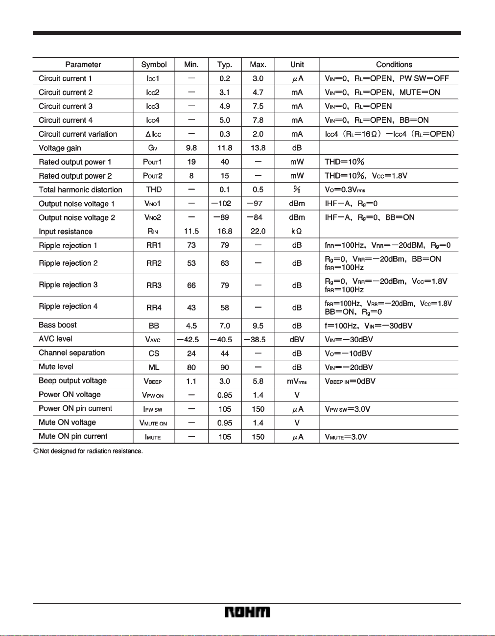
FElectrical characteristics (unless otherwise noted, Ta = 25_C, VCC = 2.4V, RL = 16Ω, f = 1kHz, and BB = OFF)
585
Page 4
Audio ICs BA3574BFS
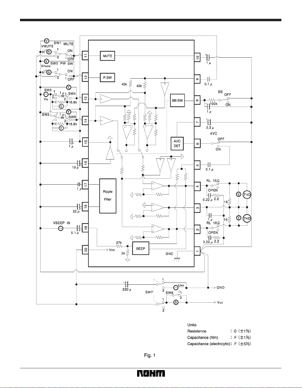
Measurement circuit
586
Page 5

Audio ICs BA3574BFS
Measurement circuit switch table
587
Page 6

Audio ICs BA3574BFS
Application example 1
588
Page 7

Audio ICs BA3574BFS
Application example 2
589
Page 8

Audio ICs BA3574BFS
Application example 3
590
Page 9

Audio ICs BA3574BFS
Operation notes
(1) Application circuits
Provided the recommended circuit constants are used,
the application circuits should function correctly. However, we recommend that you confirm the characteristics of
the circuits in actual use. If you change the circuit
constants, check both the static and transient characteristics of the circuit, and allow sufficient margin to accommodate variations between both ICs and external components.
In particular, the capacitors connected to the OUT 1,
OUT 2, and Vref pins must have low impedance at high
frequency .
(2) Wiring of PCB
The PCB pattern for the external components should be
designed carefully to prevent oscillation and degradation
of the circuit characteristics. Keep the wiring tracks as
short as possible, and ensure that there is no impedance
between the common connections.
(3) Recommended power supply voltage range
The curves in Fig. 5 below show the maximum allowable
power output (P
age (V
CC) for different values of ambient temperature
(Ta). When V
O (Max.)/ch) plotted against the supply volt-
CC y 3.6V, operate the IC in the region be-
low the dotted line, and do not exceed it.
If the maximum allowable power output for each channel
O (Max.)/ ch) is exceed, the internal power consumption
(P
will exceed the power dissipation capacity of the package, and destroy the IC.
(4) Switching noise prevention
Operate the BA3574BFS according to the timing diagram given in Fig. 6 below to prevent a “pop” sound from
being output to the headphones.
(5) BIAS OUT (pin 15)
The internal operating point voltage of the BA3574BFS
is supplied from BIAS OUT (pin 15). The current capacity
is limited, so do not use this as the operating point for external circuits.
591
Page 10

Audio ICs BA3574BFS
Electrical characteristics curves
592
Page 11

Audio ICs BA3574BFS
External dimensions (Units: mm)
593
 Loading...