

Page 1
Alpha Industries, Inc. [781] 935-5150 • Fax [617] 824-4579 • Email sales@alphaind.com • www.alphaind.com 1
Specifications subject to change without notice. 1/01A
24–30 GHz GaAs MMIC
Low Noise Amplifier
Features
■ Single Bias Supply Operation (4.5 V)
■ 3.0 dB Typical Noise Figure at 28 GHz
■ 17 dB Typical Small Signal Gain
■ 0.25 µm Ti/Pd/Au Gates
■ 100% On-Wafer RF, DC and Noise
Figure Testing
■ 100% Visual Inspection to MIL-STD-883
MT 2010
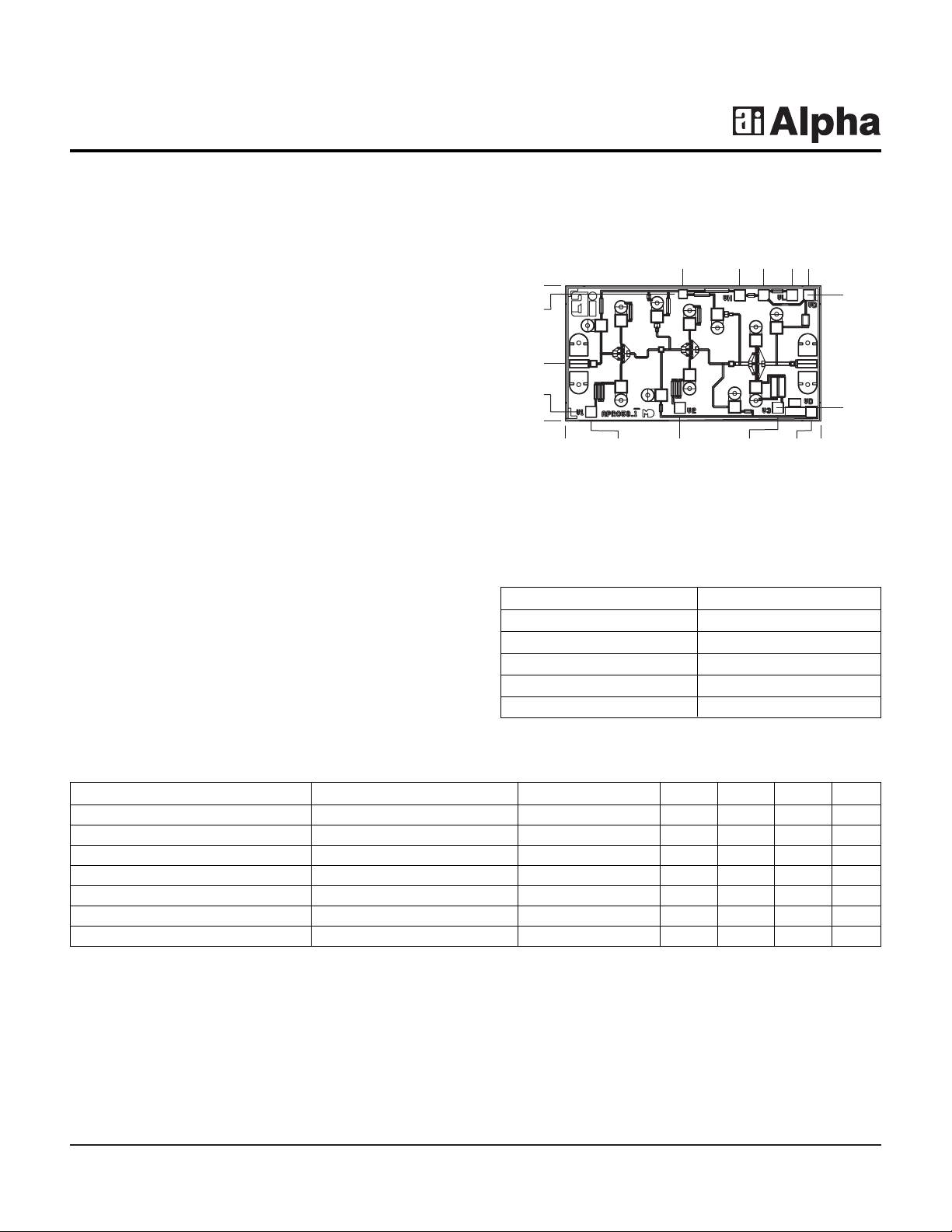
Chip Outline
AA028N1-00
Description
Alpha’s three-stage reactively-matched 24–30 GHz
MMIC low noise amplifier has typical small signal gain of
17 dB with a typical noise figure of 3.0 dB at 28 GHz.
The chip uses Alpha’s prov en 0.25 µm lo w noise PHEMT
technology, and is based upon MBE layers and electron
beam lithography for the highest uniformity and
repeatability. The FETs employ surface passivation to
ensure a rugged reliable part with through-substrate via
holes and gold-based backside metallization to facilitate
a conductive epoxy die attach process.
Parameter Condition Symbol Min. Typ.
3
Max. Unit
Drain Current I
DS
24 50 mA
Small Signal Gain F = 24–30 GHz G 15 17 dB
Noise Figure F = 28 GHz NF 3.0 3.5 dB
Input Return Loss F = 24–30 GHz RL
I
-11 -6 dB
Output Return Loss F = 24–30 GHz RL
O
-14 -10 dB
Output Power at 1 dB Gain Compression
1
F = 28 GHz P
1 dB
7 dBm
Thermal Resistance
2
Θ
JC
92 °C/W
Electrical Specifications at 25°C (VDS= 4.5 V)
0.000
0.000
0.530
0.087
0.235
1.056
2.355
2.268
1.957
0.124
1.250
1.084
1.605
1.829
2.091
2.245
1.162
1.172
Dimensions indicated in mm.
All DC (V) pads are 0.1 x 0.1 mm and RF In, Out pads are 0.07 mm wide.
Chip thickness = 0.1 mm.
Characteristic Value
Operating Temperature (TC) -55°C to +90°C
Storage Temperature (TST) -65°C to +150°C
Bias Voltage (VD)6 V
DC
Power In (PIN) 10 dBm
Junction Temperature (TJ) 175°C
Absolute Maximum Ratings
1. Not measured on a 100% basis.
2. Calculated value based on measurement of discrete FET.
3.Typical represents the median parameter value across the specified
frequency range for the median chip.
Page 2
24–30 GHz GaAs MMIC Low Noise Amplifier AA028N1-00
2 Alpha Industries, Inc. [781] 935-5150 • Fax [617] 824-4579 • Email sales@alphaind.com • www.alphaind.com
Specifications subject to change without notice. 1/01A
20 24 28 32
Frequency (GHz)
Typical Small Signal Performance
S-Parameters (V
D
= 4.5 V)
(dB)
20
10
0
-10
-20
-30
-40
-50
S
21
S
11
S
22
S
12
Typical Gain and Noise Figure
Performance for Three Bias Conditions
Frequency (GHz)
Noise Figure (dB)
20 22 24 26 28 30 32
2
3
4
5
6
7
8
9
10
13
14
15
16
17
18
19
20
21
NF 4.5 V
NF 2.5 V
NF* 2.5 V 5.0 V
Gain 4.5 V
Gain 2.5 V
Gain* 2.5 V 5.0 V
Gain (dB)
Typical Gain and Noise Figure
Performance vs. Drain Bias (V
D1
= VD2)
VD1 and VD2 (V)
2
4
6
8
10
12
14
16
18
20
1.0 2.0 3.0 4.0 5.0 6.0
28 GHz Gain (dB) and
28 GHz Noise Figure (dB)
16
19
22
25
28
31
34
37
40
43
Drain Current (mA)
Gain
NF
I
D
Typical Performance Data
V
D2
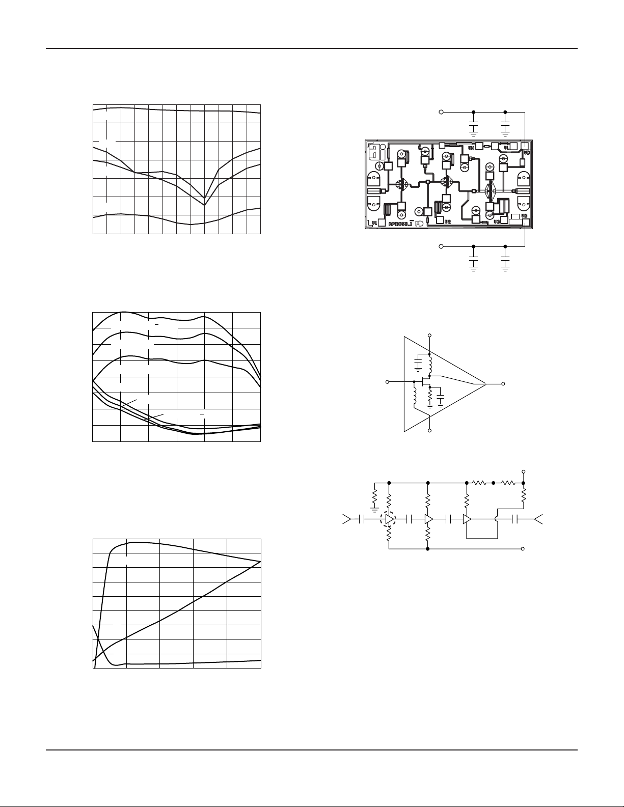
RF IN RF OUT
.01 µF 50 pF
.01 µF 50 pF
V
D1
Bias Arrangement
D
G
Detail A
RF IN RF OUT
G
D
G
D
G
D
V
D2
V
D1
SEE
DETAIL
A
Circuit Schematic
For biasing on, adjust VDSfrom zero to the desired value
(4.5 V recommended).For biasing off, reverse the biasing on procedure.
*Special Bias:V
D1
= 2.5 V, VD2= 5.0 V
 Loading...