

Page 1
93C06/46
256 Bit/1K 5.0V CMOS Serial EEPROM
FEATURES
• Low power CMOS technology
• 16 bit memory organization
- 6 x 16 bit organization (93C06)
- 64 x 16 bit organization (93C46)
• Single 5 volt only operation
• Self-timed ERASE and WRITE cycles
• Automatic ERASE before WRITE
• Power on/off data protection circuitry
• 1,000,000 ERASE/WRITE cycles guaranteed
• Data Retention > 200 years
• 8-pin DIP or SOIC package
• Available for extended temperature ranges:
- Commercial: 0˚C to +70˚C
- Industrial: -40˚C to +85˚C
- Automotive: -40˚C to +125˚C
• 2 ms program cycle time
DESCRIPTION
The Microchip Technology Inc. 93C06/46 family of
Serial Electrically Erasable PROMs are configured in a
x16 organization. Advanced CMOS technology makes
these devices ideal for low-power non-volatile memory
applications. The 93C06/46 is available in the standard
8-pin DIP and surface mount SOIC packages. The
93C46X comes as SOIC only.
These devices offer fast (1 ms) byte write and extended
(-40˚C to +125˚C) temperature operation. It is recommended that all other applications use Microchip’s
93LC46.
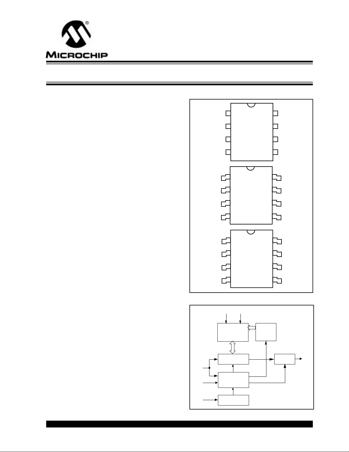
PACKAGE TYPE
DIP
1
CS
DO
2
93C06
93C46
3
DI
4
CLK
SOIC
CC
1
2
3
4
1
2
3
4
93C06
93C46
93C46X
CS
CLK
DI
DO
NC
V
CS
CLK
BLOCK DIAGRAM
V
CC VSS
8
V
CC
7
NC
6
NC
5
V
SS
8
V
CC
7
NC
6
NC
5
V
SS
8
NC
7
V
SS
6
DO
5
DI
MEMORY
ARRAY
DATA REGISTER
DI
MODE
DECODE
CS
CLK
1995 Microchip Technology Inc. DS11179C-page 1
LOGIC
CLOCK
GENERATOR
ADDRESS
DECODER
OUTPUT
BUFFER
DO
Page 2
93C06/46
µ
1.0 ELECTRICAL CHARACTERISTICS
1.1 Maximum Ratings*
V
............................................................................7.0V
CC
SS
All inputs and outputs w.r.t. V
.........-0.6V to V
Storage temperature................................-65˚C to +150˚C
CC
+1.0V
TABLE 1-1: PIN FUNCTION TABLE
Name Function
CS Chip Select
CLK Serial Clock
DI Data In
Ambient temperature with power applied .-65˚C to +125C
Soldering temperature of leads (10 seconds)........+300˚C
ESD protection on all pins ......................................... 4 kV
*Notice: Stresses above those listed under “Maximum ratings”
may cause permanent damage to the device. This is a stress rating only and functional operation of the device at those or any
other conditions above those indicated in the operational listings
of this specification is not implied. Exposure to maximum rating
conditions for extended periods may affect device reliability.
DO Data Out
SS
V
Ground
NC No Connect; No Internal
Connection
V
CC
+5V Power Supply
TABLE 1-2: DC CHARACTERISTICS
V
= +5V ( ± 10%) Commercial: Tamb = 0˚C to +70˚C
CC
Industrial: Tamb = -40˚C to +85˚C
Automotive: Tamb = -40˚C to +125˚C (Note 3)
Parameter Symbol Min Max Units Conditions
V
CC
detector threshold V
High level input voltage V
Low level input voltage V
High level output voltage V
Low level output voltage V
Input leakage current I
Output leakage current I
Pin capacitance
(all inputs/outputs)
TH
IH
IL
OH
OL
LI
LO
C
IN
, C
OUT
2.8 4.5 V
2.0 V
CC
+ 1 V
-0.3 0.8 V
2.4 — V I
— 0.4 V I
—10
—10
µ
AV
µ
AV
— 7 pF V
= -400 µ A
OH
= 3.2 mA
OL
= 0V to V
IN
= 0V to V
OUT
IN
/V
OUT
Tamb = +25˚C, f = 1 MHz
(Note 1)
CC
(Note 1)
CC
= 0V (Note 2)
Operating current (all modes) I
Standby current I
write — 4 mA F
CC
CCS
— 100
CLK
A CS = 0V, V
Note 1: Internal resistor pull-up at Pin 6.
Note 2: This parameter is periodically sampled and not 100% tested.
Note 3: For operation above 85˚C, endurance is rated at 10,000 ERASE/WRITE cycles.
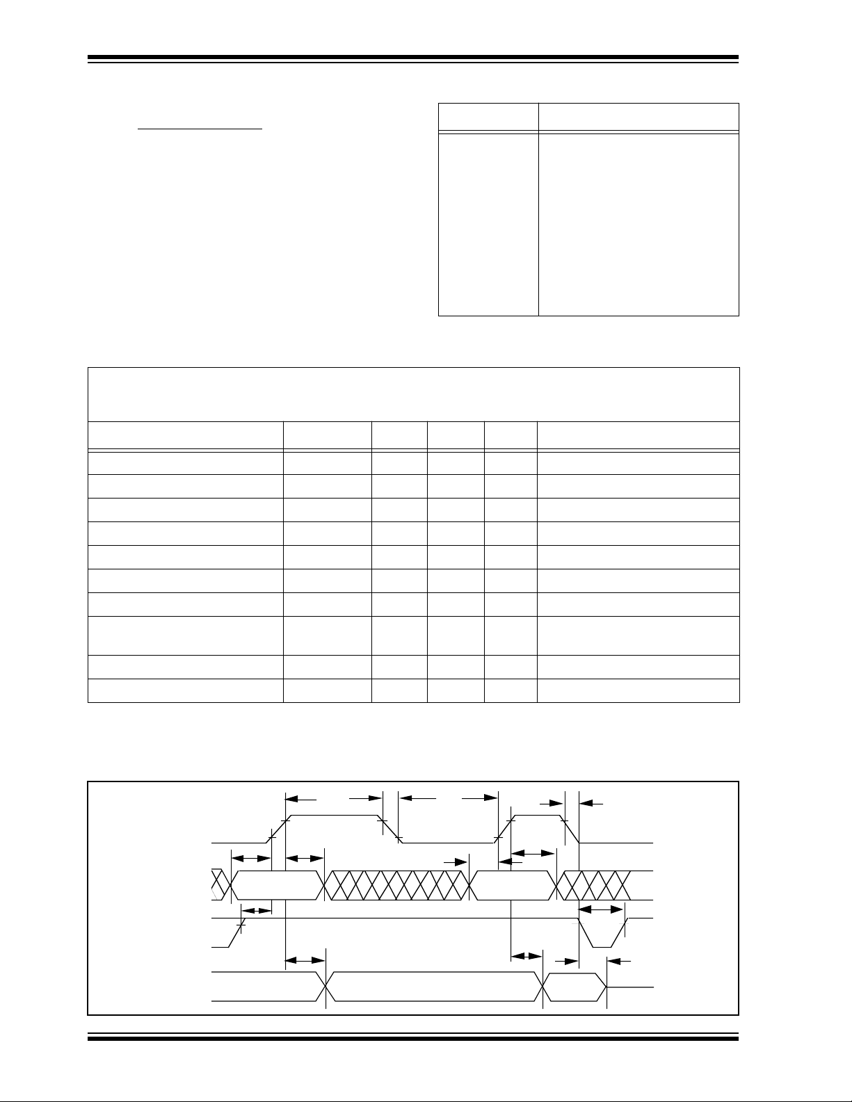
FIGURE 1-1: SYNCHRONOUS DATA TIMING
TCKH TCKL
CLK
TDIH
TDIH
TPD
VALID
T
DIS
VALID
TPD
VALID
DS11179C-page 2
DI
CS
DO
TDIS
VALID
TCSS
= 1 MHz, V
CC
TCSH
TCZ
1995 Microchip Technology Inc.
CC
= 5.5V
TCSL
HIGH
Z
= 5.5V
Page 3
TABLE 1-3: AC CHARACTERISTICS
Parameter Symbol Min Max Units Conditions
93C06/46
Clock frequency F
Clock high time T
Clock low time T
Chip select setup time T
Chip select hold time T
Chip select low time T
Data input setup time T
Data input hold time T
Data output delay time T
Data output disable time (from CS = low) T
Data output disable time (from last clock) T
Status valid time T
Program cycle time (Auto Erase and Write) T
Erase cycle time T
CLK
CKH
CKL
CSS
CSH
CSL
DIS
DIH
PD
CZ
DDZ
SV
WC
EC
2.0 PIN DESCRIPTION
2.1 Chip Select (CS)
A HIGH level selects the device. A LOW level deselects the device and forces it into standby mode. However, a programming cycle which is already initiated
and/or in progress will be completed, regardless of the
CS input signal. If CS is brought LOW during a program cycle, the device will go into standby mode as
soon as the programming cycle is completed.
CS must be LOW for 100 ns minimum (T
consecutive instructions. If CS is LOW, the internal
control logic is held in a RESET status.
2.2 Serial Clock (CLK)
The Serial Clock is used to synchronize the communication between a master device and the 93C06/46.
Opcode, address, and data bits are clocked in on the
positive edge of CLK. Data bits are also clocked out on
the positive edge of CLK.
CLK can be stopped anywhere in the transmission
sequence (at HIGH or LOW level) and can be continued anytime (with respect to clock HIGH time (T
and clock LOW time (T
master freedom in preparing opcode, address and
data.
CLK is a “Don't Care” if CS is LOW (device deselected).
If CS is HIGH, but START condition has not been
detected, any number of clock cycles can be received
by the device without changing its status. (i.e., waiting
for START condition).
CKL
). This gives the controlling
CSL
) between
CKH
500 — ns
500 — ns
50 — ns
0— ns
100 — ns
100 — ns
100 — ns
— 400 ns CL = 100 pF
0 100 ns CL = 100 pF
0 400 ns CL = 100 pF
— 100 ns CL = 100 pF
—215ms
—1 ms
CLK cycles are not required during the self-timed
WRITE (i.e., auto ERASE/WRITE) cycle.
After detection of a start condition, the specified number of clock cycles (respectively LOW to HIGH transitions of CLK) must be provided. These clock cycles are
required to clock in all required opcode, address, and
data bits before an instruction is executed (see instruction set truth table). CLK and DI then become “Don't
Care” inputs waiting for a new start condition to be
detected.
Note: CS must go LOW between consecutive
2.3 Data In (DI)
Data In is used to clock in a START bit, opcode,
address, and data synchronously with the CLK input.
2.4 Data Out (DO)
Data Out is used in the READ mode to output data
synchronously with the CLK input (T
tive edge of CLK).
This pin also provides READY/BUSY
)
tion during ERASE and WRITE cycles. READY/BUSY
status information is available on the DO pin if CS is
brought HIGH after being LOW for minimum chip select
LOW time (T
clocked in the last DI bit (D0 for WRITE, A0 for ERASE)
and an ERASE or WRITE operation has been initiated.
1 MHz
ms For ERAL and WRAL
instructions.
PD
) from the falling edge of the CLK which
CSL
after the posi-
status informa-
1995 Microchip Technology Inc. DS11179C-page 3
Page 4
93C06/46
The status signal is not available on DO, if CS is held
LOW or HIGH during the entire WRITE or ERASE
cycle. In all other cases DO is in the HIGH-Z mode. If
status is checked after the WRITE/ERASE cycle, a
pull-up resistor on DO is required to read the READY
signal.
Care must be taken with the leading dummy zero which
is outputted after a READ command has been
detected. Also, the controlling device must not drive
the DI/DO bus during Erase and Write cycles if the
READY/BUSY
status information is outputted by the
93C06/46.
DI and DO can be connected together to perform a 3wire interface (CS, CLK, DI/DO).
INSTRUCTION SET - 93C06
Instruction Start BIT
READ 1 1 0 0 0 A3 A2 A1 A0 — D15 - D0 25
WRITE 1 0 1 0 0 A3 A2 A1 A0 D15 - D0 (RDY/BSY
ERASE 1 1 1 0 0 A3 A2 A1 A0 — (RDY/BSY)9
EWEN 1 0 0 1 1 X X X X — High-Z 9
EWDS 1 0 0 0 0 X X X X — High-Z 9
ERAL 1 0 0 1 0 X X X X — (RDY/BSY)9
WRAL 1 0 0 0 1 X X X X D15 - D0 (RDY/BSY)25
Opcode
OP1 OP2
Address
Number of
Data In
Data Out
Req. CLK
Cycles
)25
INSTRUCTION SET - 93C46
Instruction Start BIT
READ 1 1 0 A5 A4 A3 A2 A1 A0 — D15 - D0 25
WRITE 1 0 1 A5 A4 A3 A2 A1 A0 D15 - D0 (RDY/BSY)25
ERASE 1 1 1 A5 A4 A3 A2 A1 A0 — (RDY/BSY)9
EWEN 1 0 0 1 1 X X X X — High-Z 9
EWDS 1 0 0 0 0 X X X X — High-Z 9
ERAL 1 0 0 1 0 X X X X — (RDY/BSY)9
WRAL 1 0 0 0 1 X X X X D15 - D0 (RDY/BSY)25
Opcode
OP1 OP2
Address
Number of
Data In
Data Out
Req. CLK
Cycles
3.0 FUNCTIONAL DESCRIPTION
3.1 ST
The START bit is detected by the device if CS and DI
are both HIGH with respect to the positive edge of CLK
for the first time.
Before a STAR T condition is detected, CS, CLK, and DI
may change in any combination (except to that of a
STAR T condition), without resulting in any device operation (READ, WRITE, ERASE, EWEN, EWDS, ERAL,
and WRAL). As soon as CS is HIGH, the device is no
longer in the standby mode.
An instruction following a START condition will only be
executed if the required amount of opcode, address
and data bits for any particular instruction is clocked in.
After execution of an instruction (i.e., clock in or out of
the last required address or data bit) CLK and DI
become don't care bits until a new start condition is
detected.
3.2 DI/DO
It is possible to connect the Data In and Data Out pins
together. However, with this configuration it is possible
for a “bus conflict” to occur during the “dummy zero”
ART Condition
that precedes the READ operation, if A0 is a logic HIGH
level. Under such a condition the voltage level seen at
Data Out is undefined and will depend upon the relative
impedances of Data Out and the signal source driving
A0. The higher the current sourcing capability of A0,
the higher the voltage at the Data Out pin.
3.3 Data Protection
During power-up, all modes of operation are inhibited
until V
CC
has reached 2.8V. During power-down, the
source data protection circuitry acts to inhibit all modes
when V
The EWEN and EWDS commands give additional protection against accidentally programming during normal operation.
After power-up, the device is automatically in the
EWDS mode. Therefore, an EWEN instruction must be
performed before any ERASE or WRITE instruction
can be executed. After programming is completed, the
EWDS instruction offers added protection against unintended data changes.
has fallen below 2.8V.
CC
DS11179C-page 4
1995 Microchip Technology Inc.
Page 5
93C06/46
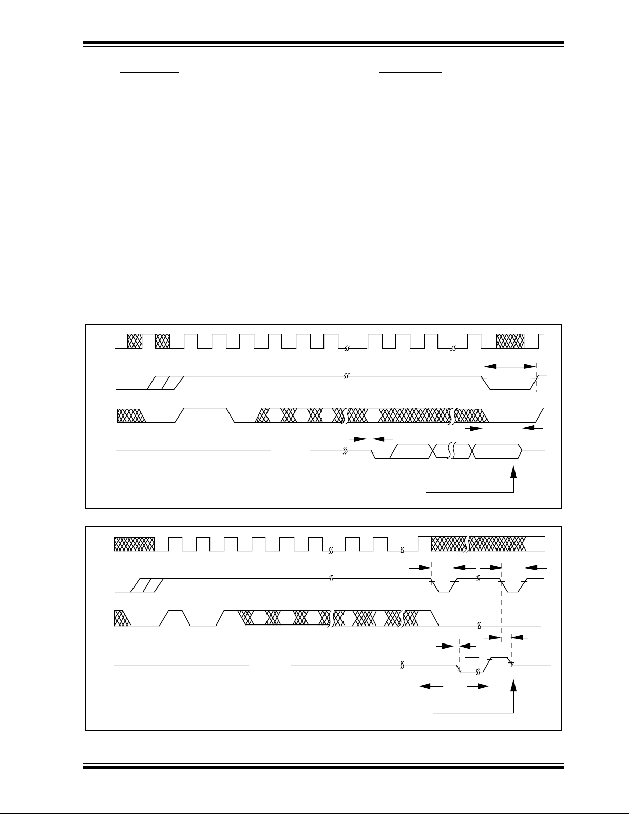
3.4 READ Mode
The READ instruction outputs the serial data of the
addressed memory location on the DO pin. A dummy
bit (logical 0) precedes the 16-bit output string. The
output data changes during the HIGH state of the system clock (CLK). The dummy bit is output TPD after
the positive edge of CLK, which was used to clock in
the last address bit (A0). Therefore, care must be
taken if DI and DO are connected together as a bus
contention will occur for one clock cycle if A0 has been
a one.
DO will go into HIGH-Z mode with the positive edge of
the next CLK cycle. This follows the output of the last
data bit D0 or the low going edge of CS, which ever
occurs first.
DO remains stable between CLK cycles for an unlimited time as long as CS stays HIGH.
The most significant data bit (D15) is always output
first, followed by the lower significant bits (D14 - D0).
FIGURE 3-1: READ MODE
CLK
3.5 WRITE Mode
The WRITE instruction is followed by 16 bits of data
which are written into the specified address. The most
significant data bit (D15) has to be clocked in first, followed by the lower significant data bits (D14 – D0). If
a WRITE instruction is recognized by the device and all
data bits have been clocked in, the device performs an
automatic ERASE cycle on the specified address
before the data are written. The WRITE cycle is completely self-timed and commences automatically after
the rising edge of the CLK for the last data bit (D0).
The WRITE cycle takes 2 ms maximum.
CS
OP1SB A5 A0
DI
10
DO
FIGURE 3-2: WRITE MODE
CLK
CS
SB A3
DI
101
DO
OP2 A4 A3
1
OP2
HIGH - Z
HIGH - Z
A4A5OP1
TPD
0
A0 D15 D0
TDDZ
D0D15
NEW INSTRUCTION
OR STANDBY (CS = 0)
TCSL
STATUS
CHECK
TSV
BSY
RDY
TCSL
TCSL
TDDZ
TWC
NEW INSTRUCTION
OR STANDBY (CS = 0)
1995 Microchip Technology Inc. DS11179C-page 5
Page 6
93C06/46
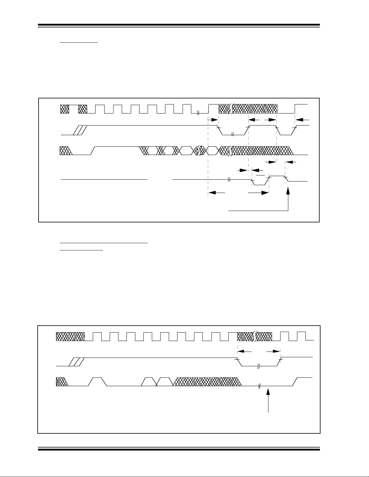
3.6 ERASE Mode
The ERASE instruction forces all the data bits of the
specified address to logical "1s". The ERASE cycle is
completely self-timed and commences automatically
after the last address bit has been clocked in.
The ERASE cycle takes 1 ms maximum.
FIGURE 3-3: ERASE MODE
CLK
CS
OP2SB
DI
1
DO
11
HIGH - Z
3.7 ERASE/WRITE Enable/Disable (EWEN, EWDS)
The device is automatically in the ERASE/WRITE
Disable mode (EWDS) after power-up. Therefore,
an EWEN instruction has to be performed before any
ERASE, WRITE, ERAL, WRAL instruction is executed by the device. For added data protection, the
device should be put in the ERASE/WRITE Disable
mode (EWDS) after programming operations are
completed.
A4A5OP1
A3 A0
TCSL
STATUS
CHECK
TSV
BSY
TEC
NEW INSTRUCTION
OR STANDBY (CS = 0)
TCSL
TDDZ
RDY
FIGURE 3-4: ERASE/WRITE ENABLE/DISABLE
CLK
CS
OP1SB
OP2
DI
10000
DS11179C-page 6
11
XX
XX
(EWDS)
(EWEN)
TCSL
SB
NEW INSTRUCTION
OR STANDBY (CS = 0)
1995 Microchip Technology Inc.
Page 7
93C06/46
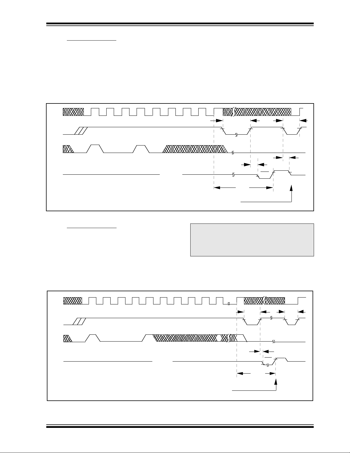
3.8 ERASE
All (ERAL)
The entire chip will be erased to logical "1s" if this
instruction is received by the device and it is in the
EWEN mode. The ERAL cycle is completely self-timed
and commences after the last dummy address bit has
been clocked in.
ERAL takes 15 ms maximum.
FIGURE 3-5: ERASE ALL
CLK
CS
OP1
SB
DI
11000XX
DO
OP2
HIGH - Z
TCSL
STATUS
CHECK
XX
TSV
TWC
NEW INSTRUCTION
OR STANDBY (CS = 0)
T
BSY
DDZ
TCSL
RDY
3.9 WRITE
All (WRAL)
The entire chip will be written with the data specified in
that command. The WRAL cycle is completely selftimed and commences after the rising edge of the CLK
for the last data bit (DO). WRAL takes 15 ms maximum.
FIGURE 3-6: WRITE ALL
CLK
CS
OP1SB OP2
DI
DO
0
1
0
01
HIGH - Z
Note: The WRAL does not include an automatic
ERASE cycle for the chip. Therefore, the
WRAL instruction must be preceded by an
ERAL instruction and the chip must be in
the EWEN status in both cases.
The WRAL instruction is used for testing and/or device
initialization.
T
CSL
STATUS
TWC
CHECK
BSY
TSV
RDY
D15
X
X
XX
D0
NEW INSTRUCTION
OR STANDBY (CS = 0)
TCSL
1995 Microchip Technology Inc. DS11179C-page 7
Page 8
93C06/46
93C06/46
To order or to obtain information, e.g., on pricing or delivery, please use the listed part numbers, and refer to the factory or the listed
sales offices.
Product Identification System
93C06/46 - /P
AMERICAS
Corporate Office
Microchip T echnology Inc.
2355 West Chandler Blvd.
Chandler, AZ 85224-6199
Tel: 602 786-7200 Fax: 602 786-7277
Technical Support:
Web:
http://www.mchip.com/biz/mchip
Atlanta
Microchip T echnology Inc.
500 Sugar Mill Road, Suite 200B
Atlanta, GA 30350
Tel: 770 640-0034 Fax: 770 640-0307
Boston
Microchip T echnology Inc.
5 Mount Royal Avenue
Marlborough, MA 01752
Tel: 508 480-9990 Fax: 508 480-8575
Chicago
Microchip T echnology Inc.
333 Pierce Road, Suite 180
Itasca, IL 60143
Tel: 708 285-0071 Fax: 708 285-0075
Dallas
Microchip T echnology Inc.
14651 Dallas Parkway, Suite 816
Dallas, TX 75240-8809
Tel: 214 991-7177 Fax: 214 991-8588
Dayton
Microchip T echnology Inc.
35 Rockridge Road
Englewood, OH 45322
Tel: 513 832-2543 Fax: 513 832-2841
Los Angeles
Microchip T echnology Inc.
18201 Von Karman, Suite 455
Irvine, CA 92715
Tel: 714 263-1888 Fax: 714 263-1338
New York
Microchip T echnology Inc.
150 Motor Parkway, Suite 416
Hauppauge, NY 11788
Tel: 516 273-5305 Fax: 516 273-5335
602 786-7627
Package: P = Plastic DIP (300 mil Body)
Temperature Blank = 0°C to +70°C
Range: I = -40°C to +85°C
Device: Configuration
AMERICAS (continued)
San Jose
Microchip T echnology Inc.
2107 North First Street, Suite 590
San Jose, CA 95131
Tel: 408 436-7950 Fax: 408 436-7955
ASIA/PACIFIC
Hong Kong
Microchip T echnology
Unit No. 3002-3004, Tower 1
Metroplaza
223 Hing Fong Road
Kwai Fong, N.T. Hong Kong
Tel: 852 2 401 1200 Fax: 852 2 401 3431
Korea
Microchip T echnology
168-1, Youngbo Bldg. 3 Floor
Samsung-Dong, Kangnam-Ku,
Seoul, Korea
Tel: 82 2 554 7200 Fax: 82 2 558 5934
Singapore
Microchip T echnology
200 Middle Road
#10-03 Prime Centre
Singapore 188980
Tel: 65 334 8870 Fax: 65 334 8850
Taiwan
Microchip T echnology
10F-1C 207
Tung Hua North Road
Taipei, T aiwan, ROC
Tel: 886 2 717 7175 Fax: 886 2 545 0139
SN = Plastic SOIC (150 mil Body)
SM = Plastic SOIC (207 mil Body)
E = -40°C to +125°C
93C06 256 bit CMOS Serial EEPROM
93C46 1K CMOS Serial EEPROM
93C46X 1K CMOS Serial EEPROM in alternate pinouts (SN
package only)
93C06T CMOS Serial EEPROM (Tape and Reel)
93C46T CMOS Serial EEPROM (Tape and Reel)
93C46XT CMOS Serial EEPROM (Tape and Reel)
EUROPE
United Kingdom
Arizona Microchip Technology Ltd.
Unit 6, The Courtyard
Meadow Bank, Furlong Road
Bourne End, Buckinghamshire SL8 5AJ
T el: 44 0 1628 851077 Fax: 44 0 1628 850259
France
Arizona Microchip Technology SARL
2 Rue du Buisson aux Fraises
91300 Massy - France
Tel: 33 1 69 53 63 20 Fax: 33 1 69 30 90 79
Germany
Arizona Microchip Technology GmbH
Gustav-Heinemann-Ring 125
D-81739 Muenchen, Germany
Tel: 49 89 627 144 0 Fax: 49 89 627 144 44
Italy
Arizona Microchip Technology SRL
Centro Direzionale Colleoni
Palazzo Pegaso Ingresso No. 2
Via Paracelso 23, 20041
Agrate Brianza (MI) Italy
Tel: 39 039 689 9939 Fax: 39 039 689 9883
JAPAN
Microchip Technology Intl. Inc.
Benex S-1 6F
3-18-20, Shin Yokohama
Kohoku-Ku, Y okohama
Kanagawa 222 Japan
Tel: 81 45 471 6166 Fax: 81 45 471 6122
9/5/95
Printed in the USA, 9/95
1995, Microchip Technology Incorporated
"Information contained in this publication regarding device applications and the like is intended through suggestion only and may be superseded by updates. No representation or warranty is given and no
liability is assumed by Microchip Technology Incorporated with respect to the accuracy or use of such information, or infringement of patents arising from such use or otherwise. Use of Microchip's products
as critical components in life support systems is not authorized except with express written approval by Microchip. No licenses are conveyed, implicitly or otherwise, under any intellectual property rights."
The Microchip logo and name are registered trademarks of Microchip Technology Inc. All rights reserved. All other trademarks mentioned herein are the property of their respective companies.
DS11179C-page 8
1995 Microchip Technology Inc.
 Loading...