

Page 1

INTEGRATED CIRCUITS
80C554/83C554/87C554
80C51 8-bit microcontroller
16K/512 OTP/ROM/ROMless, 8 channel 10 bit A/D,
I2C, PWM, capture/compare, high I/O
Preliminary specification
Replaces datasheet 87C554 of 1998 Aug 14
IC20 Data Handbook
1999 Apr 07
Page 2

Philips Semiconductors Preliminary specification
80C51 8-bit microcontroller
16K/512 OTP/ROM/ROMless, 8 channel 10 bit A/D, I2C, PWM,
80C554/83C554/87C554
capture/compare, high I/O
DESCRIPTION
The 8xC554 Single-Chip 8-Bit Microcontroller is manufactured in an
advanced CMOS process and is a derivative of the 80C51
microcontroller family. The 87C554 has the same instruction set as
the 80C51. Three versions of the derivative exist:
•83C554—16k bytes programmable ROM
•80C554—ROMless version of the 83C554
•87C554—16k bytes EPROM
The 87C554 contains a 16k × 8 non-volatile EPROM, a 512 × 8
read/write data memory, five 8-bit I/O ports, one 8-bit input port, two
16-bit timer/event counters (identical to the timers of the 80C51), an
additional 16-bit timer coupled to capture and compare latches, a
15-source, four-priority-level, nested interrupt structure, an 8-input
ADC, a dual DAC pulse width modulated interface, two serial
interfaces (UART and I
oscillator and timing circuits. For systems that require extra
capability , the 8xC554 can be expanded using standard TTL
compatible memories and logic.
In addition, the 8xC554 has two software selectable modes of power
reduction—idle mode and power-down mode. The idle mode freezes
the CPU while allowing the RAM, timers, serial ports, and interrupt
system to continue functioning. Optionally, the ADC can be operated
in Idle mode. The power-down mode saves the RAM contents but
freezes the oscillator, causing all other chip functions to be
inoperative.
The device also functions as an arithmetic processor having
facilities for both binary and BCD arithmetic plus bit-handling
capabilities. The instruction set consists of over 100 instructions:
49 one-byte, 45 two-byte, and 17 three-byte. With a 16MHz crystal,
58% of the instructions are executed in 0.75µs and 40% in 1.5µs.
Multiply and divide instructions require 3µs.
2
C-bus), a “watchdog” timer and on-chip
FEATURES
•80C51 central processing unit
•16k × 8 EPROM expandable externally to 64k bytes
•An additional 16-bit timer/counter coupled to four capture registers
and three compare registers
•Two standard 16-bit timer/counters
•512 × 8 RAM, expandable externally to 64k bytes
•Capable of producing eight synchronized, timed outputs
•A 10-bit ADC with eight multiplexed analog inputs
•Fast 8-bit ADC option
•Two 8-bit resolution, pulse width modulation outputs
•Five 8-bit I/O ports plus one 8-bit input port shared with analog
inputs
2
•I
C-bus serial I/O port with byte oriented master and slave
functions
•On-chip watchdog timer
•Extended temperature ranges
•Full static operation – 0 to 16 MHz
•Operating voltage range: 2.7V to 5.5V (0 to 16MHz) and
4.5V to 5.5V (16 to 33 MHz)
•Security bits:
– ROM – 2 bits
– OTP/EPROM – 3 bits
•Encryption array – 64 bytes
•4 level priority interrupt
•15 interrupt sources
•Full-duplex enhanced UART
– Framing error detection
– Automatic address recognition
•Power control modes
– Clock can be stopped and resumed
– Idle mode
– Power down mode
•Second DPTR register
•ALE inhibit for EMI reduction
•Programmable I/O pins
•Wake-up from power-down by external interrupts
•Software reset
•Power-on detect reset
•ADC charge pump disable
•ONCE mode
•ADC active in Idle mode
1999 Apr 07
2
Page 3

Philips Semiconductors Preliminary specification
B= 0C to 70C
F = 40 C to +85 C
80C51 8-bit microcontroller
16K/512 OTP/ROM/ROMless, 8 channel 10 bit A/D, I2C, PWM,
80C554/83C554/87C554
capture/compare, high I/O
ORDERING INFORMATION
OTP/EPROM ROM ROMless TEMPERATURE °C AND PACKAGE
FREQ.
(MHz)
P87C554SBAA P83C554SBAA P80C554SBAA 0 to +70, Plastic Leaded Chip Carrier 16 SOT188–3
P87C554SFAA P83C554SFAA P80C554SFAA –40 to +85, Plastic Leaded Chip Carrier 16 SOT188–3
P ART NUMBER DERIVATION
DEVICE NUMBER (P87C554) OPERATING FREQUENCY MAX (S) TEMPERATURE RANGE (B) PACKAGE (AA)
P87C554 OTP
P83C554 ROM
S = 16 MHz
=–
P80C554 ROMless
BLOCK DIAGRAM
DRAWING
NUMBER
AA = PLCC
XTAL1
XTAL2
EA
ALE
PSEN
3
3
0
2
WR
RD
AD0-7
A8-15
T0 T1 INT0 INT1
3 3 3 3
T0, T1
TWO 16-BIT
TIMER/EVENT
COUNTERS
PARALLEL I/O
PORTS AND
EXTERNAL BUS
80C51 CORE
EXCLUDING
ROM/RAM
CPU
SERIAL
UART
PORT
V
PROGRAM
MEMORY
16k x 8
OTP/ROM
8-BIT
PORT
DD
8-BIT INTERNAL BUS
16
FOUR
16-BIT
CAPTURE
LATCHES
V
SS
DATA
MEMORY
512 x 8 RAM
COUNTERS
T2
16-BIT
TIMER/
EVENT
PWM0 PWM1
DUAL
PWM
T2
16-BIT
16
COMPARA-
TORS
WITH
REGISTERS
AV
SS
AV
AV
REF
–+
STADC
DD
ADC
COMPARA-
TOR
OUTPUT
SELECTION
ADC0-7 SDA SCL
SERIAL
2
C PORT
I
T3
WATCHDOG
TIMER
115
0
ALTERNATE FUNCTION OF PORT 0
1
ALTERNATE FUNCTION OF PORT 1
2
ALTERNATE FUNCTION OF PORT 2
1999 Apr 07
3 3
P0 P1 P2 P3 TxD RxD P5 P4 CT0I-CT3I T2 RT2 CMSR0-CMSR5
3
ALTERNATE FUNCTION OF PORT 3
4
ALTERNATE FUNCTION OF PORT 4
5
ALTERNATE FUNCTION OF PORT 5
1 1 1 4
CMT0, CMT1
3
RST EW
SU00951
Page 4

Philips Semiconductors Preliminary specification
80C51 8-bit microcontroller
16K/512 OTP/ROM/ROMless, 8 channel 10 bit A/D, I2C, PWM,
80C554/83C554/87C554
capture/compare, high I/O
PIN CONFIGURATIONS
Plastic Quad Flat Pack pin functions
80 65
1
PQFP
24
25 40
64
41
NC = Not Connected
IC = Internally Connected (do not use)
Plastic Leaded Chip Carrier pin functions
9161
60
44
4327
Pin Function
47 PSEN
48 ALE/PROG
49 EA/V
50 P0.7/AD7
51 P0.6/AD6
52 P0.5/AD5
53 P0.4/AD4
54 P0.3/AD3
55 P0.2/AD2
56 P0.1/AD1
57 P0.0/AD0
58 AVref–
59 AVref+
60 AV
61 AV
62 P5.7/ADC7
63 P5.6/ADC6
64 P5.5/ADC5
65 P5.4/ADC4
66 P5.3/ADC3
67 P5.2/ADC2
68 P5.1/ADC1
Pin Function
1 P5.0/ADC0
2V
DD
3 STADC
4 PWM0
5 PWM1
6EW
7 P4.0/CMSR0
8 P4.1/CMSR1
9 P4.2/CMSR2
10 P4.3/CMSR3
11 P4.4/CMSR4
12 P4.5/CMSR5
13 P4.6/CMT0
14 P4.7/CMT1
15 RST
16 P1.0/CT0I
17 P1.1/CT1I
18 P1.2/CT2I
19 P1.3/CT3I
20 P1.4/T2
21 P1.5/RT2
22 P1.6/SCL
23 P1.7/SDA
10
CHIP CARRIER
26
Pin Function
24 P3.0/RxD
25 P3.1/TxD
26 P3.2/INT0
27 P3.3/INT1
28 P3.4/T0
29 P3.5/T1
30 P3.6/WR
31 P3.7/RD
32 NC
33 NC
34 XTAL2
35 XTAL1
36 V
37 V
38 NC
39 P2.0/A08
40 P2.1/A09
41 P2.2/A10
42 P2.3/A11
43 P2.4/A12
44 P2.5/A13
45 P2.6/A14
46 P2.7/A15
PLASTIC
LEADED
SS
SS
Pin Function
1 P4.1/CMSR1
2 P4.2/CMSR2
3NC
4 P4.3/CMSR3
5 P4.4/CMSR4
6 P4.5/CMSR5
7
P4.6/CMT0
8 P4.7/CMT1
9 RST
10 P1.0/CT0I
11 P1.1/CT1I
12 P1.2/CT2I
13
P1.3/CT3I
14 P1.4/T2
15 P1.5/RT2
16 P1.6/SCL
17 P1.7/SDA
18 P3.0/RxD
19 P3.1/TxD
20 P3.2/INT0
PP
SS
DD
SU00208
Pin Function
21 NC
22 NC
23 P3.3/INT1
24 P3.4/T0
25 P3.5/T1
26 P3.6/WR
27 P3.7/RD
28 NC
29 NC
30 NC
31 XTAL2
32 XTAL1
33 IC
34 V
SS
35 V
SS
36 V
SS
37 NC
38 P2.0/A08
39 P2.1/A09
40 P2.2/A10
LOGIC SYMBOL
V
SS
V
DD
XTAL1
XTAL2
V
EA/
PP
ALE/PROG
PSEN
AV
SS
AV
DD
AVref+
AVref–
STADC
PWM0
PWM1
ADC0-7
PORT 5
CMSR0-5
RST
EW
PORT 4
CMT0
CMT1
Pin Function
41 P2.3/A11
42 P2.4/A12
43 NC
44 NC
45 P2.5/A13
46 P2.6/A14
47 P2.7/A15
48 PSEN
49 ALE/PROG
50 EA/V
51 P0.7/AD7
52 P0.6/AD6
53 P0.5/AD5
54 P0.4/AD4
55 P0.3/AD3
56 P0.2/AD2
57
58 P0.0/AD0
59 AVref–
60 AVref+
PP
P0.1/AD1
Pin Function
61 AV
62 NC
63 AV
64 P5.7/ADC7
65 P5.6/ADC6
66 P5.5/ADC5
67 P5.4/ADC4
68 P5.3/ADC3
69 P5.2/ADC2
70 P5.1/ADC1
71 P5.0/ADC0
72 V
73 IC
74 STADC
75 PWM0
76 PWM1
77 EW
78 NC
79 NC
80 P4.0/CMSR0
PORT 0
CT0I
CT1I
CT2I
CT3I
T2
PORT 1PORT 2PORT 3
RT2
SCL
SDA
HIGH ORDER
ADDRESS AND
RxD/DATA
TxD/CLOCK
INT0
INT1
T0
T1
WR
RD
SS
DD
DD
SU00209
LOW ORDER
ADDRESS AND
DATA BUS
DATA BUS
SU00210
1999 Apr 07
4
Page 5

Philips Semiconductors Preliminary specification
80C51 8-bit microcontroller
16K/512 OTP/ROM/ROMless, 8 channel 10 bit A/D, I2C, PWM,
80C554/83C554/87C554
capture/compare, high I/O
PIN DESCRIPTION
PIN NO.
MNEMONIC PLCC QFP TYPE NAME AND FUNCTION
V
DD
STADC 3 74 I Start ADC Operation: Input starting analog to digital conversion (ADC operation can also
PWM0 4 75 O Pulse Width Modulation: Output 0.
PWM1 5 76 O Pulse Width Modulation: Output 1.
EW 6 77 I Enable Watchdog T imer: Enable for T3 watchdog timer and disable power-down mode.
P0.0-P0.7 57-50 58-51 I/O Port 0: Port 0 is an 8-bit open-drain bidirectional I/O port. Port 0 pins that have 1s written
P1.0-P1.7
P2.0-P2.7 39-46 38-42,
P3.0-P3.7
2 72 I Digital Power Supply: Positive voltage power supply pin during normal operation, idle and
16-23 10-17 I/O Port 1: 8-bit I/O port. Alternate functions include:
16-21 10-15 I/O (P1.0-P1.5): Programmable I/O port pins.
22-23 16-17 I/O (P1.6, P1.7): Open drain port pins.
16-19 10-13 I CT0I-CT3I (P1.0-P1.3): Capture timer input signals for timer T2.
20 14 I T2 (P1.4): T2 event input.
21 15 I RT2 (P1.5): T2 timer reset signal. Rising edge triggered.
22 16 I/O SCL (P1.6): Serial port clock line I2C-bus.
23 17 I/O SDA (P1.7): Serial port data line I2C-bus.
45-47
24-31 18-20,
23-27
24 18 RxD(P3.0): Serial input port.
25 19 TxD (P3.1): Serial output port.
26 20 INT0 (P3.2): External interrupt.
27 23 INT1 (P3.3): External interrupt.
28 24 T0 (P3.4): Timer 0 external input.
29 25 T1 (P3.5): Timer 1 external input.
30 26 WR (P3.6): External data memory write strobe.
31 27 RD (P3.7): External data memory read strobe.
power-down mode.
be started by software).
to them float and can be used as high-impedance inputs. Port 0 is also the multiplexed
low-order address and data bus during accesses to external program and data memory. In
this application it uses strong internal pull-ups when emitting 1s. Port 0 is also used to input
the code byte during programming and to output the code byte during verification.
Port 1 has four modes selected on a per bit basis by writing to the P1M1 and P1M2
registers as follows:
P1M1.x P1M2.x Mode Description
0 0 Pseudo–bidirectional (standard c51 configuration; default)
0 1 Push-Pull
1 0 High impedance
1 1 Open drain
Port 1 is also used to input the lower order address byte during EPROM programming and
verification. A0 is on P1.0, etc.
I/O Port 2: 8-bit programmable I/O port.
Alternate function: High-order address byte for external memory (A08-A15). Port 2 is also
used to input the upper order address during EPROM programming and verification. A8 is
on P2.0, A9 on P2.1, through A13 on P2.5.
Port 2 has four output modes selected on a per bit basis by writing to the P2M1 and P2M2
registers as follows:
P2M1.x P2M2.x Mode Description
0 0 Pseudo–bidirectional (standard c51 configuration; default)
0 1 Push-Pull
1 0 High impedance
1 1 Open drain
I/O Port 3: 8-bit programmable I/O port. Alternate functions include:
Port 3 has four modes selected on a per bit basis by writing to the P3M1 and P3M2
registers as follows:
P3M1.x P3M2.x Mode Description
0 0 Pseudo–bidirectional (standard c51 configuration; default)
0 1 Push–Pull
1 0 High impedance
1 1 Open drain
1999 Apr 07
5
Page 6

Philips Semiconductors Preliminary specification
1
80C51 8-bit microcontroller
16K/512 OTP/ROM/ROMless, 8 channel 10 bit A/D, I2C, PWM,
80C554/83C554/87C554
capture/compare, high I/O
PIN DESCRIPTION (Continued)
PIN NO.
MNEMONIC PLCC QFP TYPE NAME AND FUNCTION
P4.0-P4.7
P5.0-P5.7 68-62,
RST 15 9 I/O Reset: Input to reset the 87C554. It also provides a reset pulse as output when timer T3
XTAL1 35 32 I Crystal Input 1: Input to the inverting amplifier that forms the oscillator, and input to the
XTAL2 34 31 O Crystal Input 2: Output of the inverting amplifier that forms the oscillator. Left open-circuit
V
SS
PSEN 47 48 O Program Store Enable: Active-low read strobe to external program memory.
ALE/PROG 48 49 O Address Latch Enable: Latches the low byte of the address during accesses to external
EA/V
PP
AV
REF–
AV
REF+
AV
SS
AV
DD
NOTE:
1. To avoid “latch-up” effect at power-on, the voltage on any pin at any time must not be higher or lower than V
respectively.
7-14 80, 1-2
4-8
7-12 80, 1-2
4-6
13, 14 7, 8 O CMT0, CMT1 (P4.6, P4.7): Timer T2 compare and toggle outputs on a match with timer T2.
71-64 I Port 5: 8-bit input port.
36, 37 34-36 I Digital ground.
49 50 I External Access: When EA is held at TTL level high, the CPU executes out of the internal
58 59 I Analog to Digital Conversion Reference Resistor: Low-end.
59 60 I Analog to Digital Conversion Reference Resistor: High-end.
60 61 I Analog Ground
61 63 I Analog Power Supply
I/O Port 4: 8-bit programmable I/O port. Alternate functions include:
O CMSR0-CMSR5 (P4.0-P4.5): Timer T2 compare and set/reset outputs on a match with
timer T2.
Port 4 has four modes selected on a per bit basis by writing to the P4M1 and P4M2
registers as follows:
P4M1.x P4M2.x Mode Description
0 0 Pseudo-bidirectional (standard c51 configuration; default)
0 1 Push-Pull
1 0 High impedance
1 1 Open drain
ADC0-ADC7 (P5.0-P5.7): Alternate function: Eight input channels to the ADC.
overflows.
internal clock generator. Receives the external clock signal when an external oscillator is
used.
when an external clock is used.
memory. It is activated every six oscillator periods. During an external data memory
access, one ALE pulse is skipped. ALE can drive up to eight LS TTL inputs and handles
CMOS inputs without an external pull-up. This pin is also the program pulse input (PROG)
during EPROM programming.
program ROM provided the program counter is less than 16,384. When EA is held at TTL
low level, the CPU executes out of external program memory. EA is not allowed to float.
This pin also receives the 12.75V programming supply voltage (VPP) during EPROM
programming.
+ 0.5V or VSS – 0.5V,
DD
1999 Apr 07
6
Page 7
Philips Semiconductors Preliminary specification
80C51 8-bit microcontroller
16K/512 OTP/ROM/ROMless, 8 channel 10 bit A/D, I2C, PWM,
80C554/83C554/87C554
capture/compare, high I/O
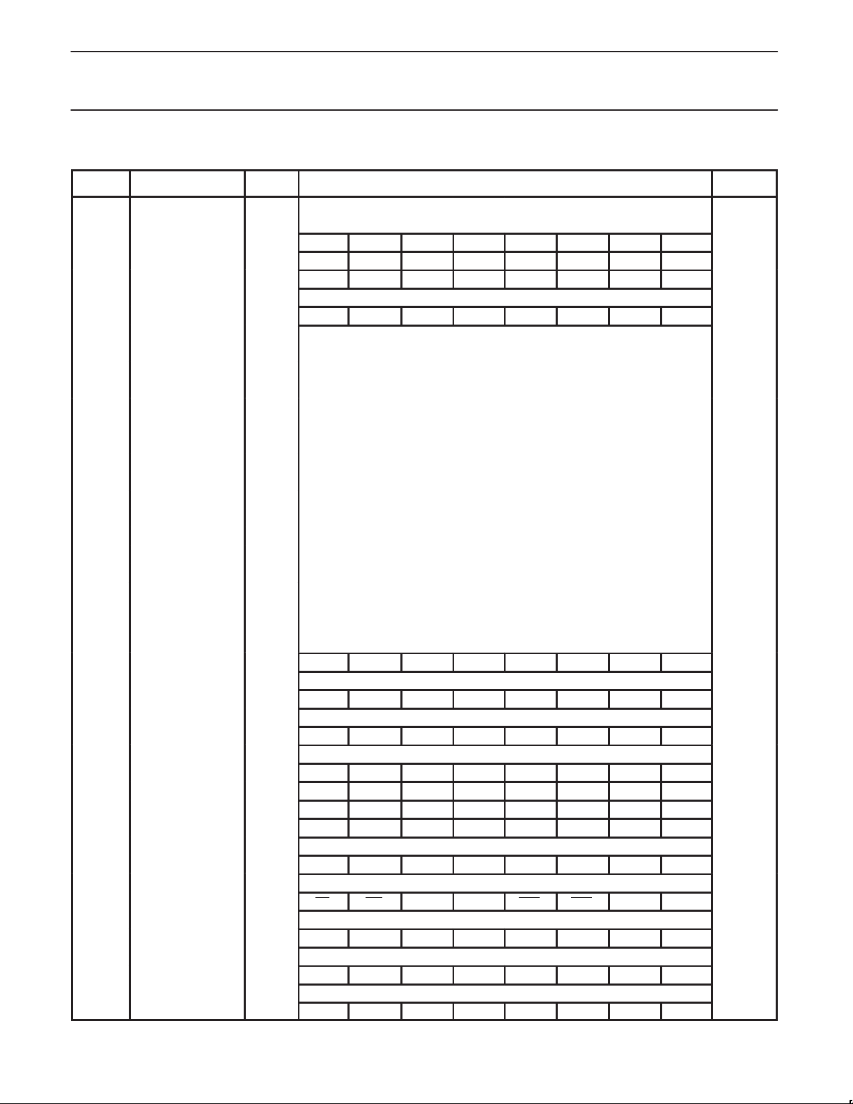
Table 1. 87C554 Special Function Registers
SYMBOL DESCRIPTION
ACC* Accumulator E0H E7 E6 E5 E4 E3 E2 E1 E0 00H
ADCH# A/D converter high C6H xxxxxxxxB
ADCON# A/D control C5H ADC.1 ADC.0 ADEX ADCI ADCS AADR2 AADR1 AADR0 xx000000B
AUXR Auxillary 8EH – – – – – LVADC EXTRAM A0 xxxxx110B
AUXR1 Auxillary A2H ADC8 AIDL SRST GF2 WUPD O – DPS 000000x0B
B* B register F0H F7 F6 F5 F4 F3 F2 F1 F0 00H
CTCON# Capture control EBH CTN3 CTP3 CTN2 CTP2 CTN1 CTP1 CTN0 CTP0 00H
CTH3# Capture high 3 CFH xxxxxxxxB
CTH2# Capture high 2 CEH xxxxxxxxB
CTH1# Capture high 1 CDH xxxxxxxxB
CTH0# Capture high 0 CCH xxxxxxxxB
CMH2# Compare high 2 CBH 00H
CMH1# Compare high 1 CAH 00H
CMH0# Compare high 0 C9H 00H
CTL3# Capture low 3 AFH xxxxxxxxB
CTL2# Capture low 2 AEH xxxxxxxxB
CTL1# Capture low 1 ADH xxxxxxxxB
CTL0# Capture low 0 ACH xxxxxxxxB
CML2# Compare low 2 ABH 00H
CML1# Compare low 1 AAH 00H
CML0# Compare low 0 A9H 00H
DPTR:
DPH
DPL
IEN0*# Interrupt enable 0 A8H EA EAD ES1 ES0 ET1 EX1 ET0 EX0 00H
IEN1*# Interrupt enable 1 E8H ET2 ECM2 ECM1 ECM0 ECT3 ECT2 ECT1 ECT0 00H
IP0*# Interrupt priority 0 B8H – PAD PS1 PS0 PT1 PX1 PT0 PX0 x0000000B
IP0H Interrupt priority 0 high B7H – PADH PS1H PS0H PT1H PX1H PT0H PX0H x0000000B
IP1*# Interrupt priority1 F8H PT2 PCM2 PCM1 PCM0 PCT3 PCT2 PCT1 PCT0 00H
IP1H Interrupt priority 1 high F7H PT2H PCM2H PCM1H PCM0H PCT3H PCT2H PCT1H PCT0H 00H
P5# Port 5 C4H ADC7 ADC6 ADC5 ADC4 ADC3 ADC2 ADC1 ADC0 xxxxxxxxB
P4#* Port 4 C0H CMT1 CMT0 CMSR5 CMSR4 CMSR3 CMSR2 CMSR1 CMSR0 FFH
P3* Port 3 B0H RD WR T1 T0 INT1 INT0 TXD RXD FFH
P2* Port 2 A0H A15 A14 A13 A12 A11 A10 A9 A8 FFH
P1* Port 1 90H SDA SCL RT2 T2 CT3I CT2I CT1I CT0I FFH
P0* Port 0 80H AD7 AD6 AD5 AD4 AD3 AD2 AD1 AD0 FFH
Data pointer
(2 bytes):
Data pointer high
Data pointer low
DIRECT
ADDRESS
83H
82H
MSB LSB
AF AE AD AC AB AA A9 A8
EF EE ED EC EB EA E9 E8
BF BE BD BC BB BA B9 B8
FF FE FD FC FB FA F9 F8
C7 C6 C5 C4 C3 C2 C1 C0
B7 B6 B5 B4 B3 B2 B1 B0
A7 A6 A5 A4 A3 A2 A1 A0
97 96 95 94 93 92 91 90
87 86 85 84 83 82 81 80
BIT ADDRESS, SYMBOL, OR ALTERNATIVE PORT FUNCTION
00H
00H
RESET
VALUE
1999 Apr 07
7
Page 8

Philips Semiconductors Preliminary specification
80C51 8-bit microcontroller
16K/512 OTP/ROM/ROMless, 8 channel 10 bit A/D, I2C, PWM,
80C554/83C554/87C554
capture/compare, high I/O
00H
00H
00H
00H
00H
00H
RESET
VALUE
SYMBOL
P1M1 Port 1 output mode 1 92H xx000000B
P1M2 Port 1 output mode 2 93H xx000000B
P2M1 Port 2 output mode 1 94H 00H
P2M2 Port 2 output mode 2 95H 00H
P3M1 Port 3 output mode 1 9AH 00H
P3M2 Port 3 output mode 2 9BH 00H
P4M1 Port 4 output mode 1 9CH 00H
P4M2 Port 4 output mode 2 9DH 00H
PCON Power control 87H SMOD1 SMOD0 POF WLE GF1 GFO PD IDL 00x00000B
PSW Program status word D0H CY AC FO RS1 RS0 OV F1 P 00H
PWMP# PWM prescaler FEH 00H
PWM1# PWM register 1 FDH 00H
PWM0# PWM register 0 FCH 00H
RTE# Reset/toggle enable EFH TP47 TP46 RP45 RP44 RP43 RP42 RP41 RP40 00H
S0ADDR Serial 0 slave address F9H 00H
S0ADEN Slave address mask B9H 00H
S0BUF Serial 0 data buffer 99H xxxxxxxxB
S0CON* Serial 0 control 98H SM0/FE SM1 SM2 REN TB8 RB8 TI RI 00H
S1ADR# Serial 1 address DBH SLAVE ADDRESS GC 00H
SIDAT# Serial 1 data DAH 00H
S1STA# Serial 1 status D9H SC4 SC3 SC2 SC1 SC0 0 0 0 F8H
SICON#* Serial 1 control D8H CR2 ENS1 STA ST0 SI AA CR1 CR0 00H
SP Stack pointer 81H 07H
STE# Set enable EEH TG47 TG46 SP45 SP44 SP43 SP42 SP41 SP40 C0H
TH1
TH0
TL1
TL0
TMH2#
TML2#
TMOD Timer mode 89H GATE C/T M1 M0 GATE C/T M1 M0 00H
TCON* Timer control 88H TF1 TR1 TF0 TR0 IE1 IT1 IE0 IT0 00H
TM2CON# Timer 2 control EAH T2IS1 T2IS0 T2ER T2B0 T2P1 T2P0 T2MS1 T2MS0 00H
TM2IR#* Timer 2 int flag reg C8H T20V CMI2 CMI1 CMI0 CTI3 CTI2 CTI1 CTI0 00H
T3# Timer 3 FFH 00H
DESCRIPTION
Timer high 1
Timer high 0
Timer low 1
Timer low 0
Timer high 2
Timer low 2
DIRECT
ADDRESS
8DH
8CH
8BH
8AH
EDH
ECH
MSB LSB
9F 9E 9D 9C 9B 9A 99 98
DF DE DD DC DB DA D9 D8
8F 8E 8D 8C 8B 8A 89 88
CF CE CD CC CB CA C9 C8
BIT ADDRESS, SYMBOL, OR ALTERNATIVE PORT FUNCTION
* SFRs are bit addressable.
# SFRs are modified from or added to the 80C51 SFRs.
1999 Apr 07
8
Page 9
Philips Semiconductors Preliminary specification
80C51 8-bit microcontroller
16K/512 OTP/ROM/ROMless, 8 channel 10 bit A/D, I2C, PWM,
80C554/83C554/87C554
capture/compare, high I/O
OSCILLA T OR CHARACTERISTICS
XTAL1 and XTAL2 are the input and output, respectively , of an
inverting amplifier . The pins can be configured for use as an on-chip
oscillator, as shown in the logic symbol.
To drive the device from an external clock source, XTAL1 should be
driven while XTAL2 is left unconnected. There are no requirements
on the duty cycle of the external clock signal, because the input to
the internal clock circuitry is through a divide-by-two flip-flop.
However, minimum and maximum high and low times specified in
the data sheet must be observed.
RESET
A reset is accomplished by either (1) externally holding the RST pin
high for at least two machine cycles (24 oscillator periods) or (2)
internally by an on-chip power-on detect (POD) circuit which detects
V
ramping up from 0V .
CC
To insure a good external power-on reset, the RST pin must be high
long enough for the oscillator to start up (normally a few
milliseconds) plus two machine cycles. The voltage on V
RST pin must come up at the same time for a proper startup.
For a successful internal power-on reset, the V
voltage must
CC
ramp up from 0V smoothly at a ramp rate greater than 5V/100 ms.
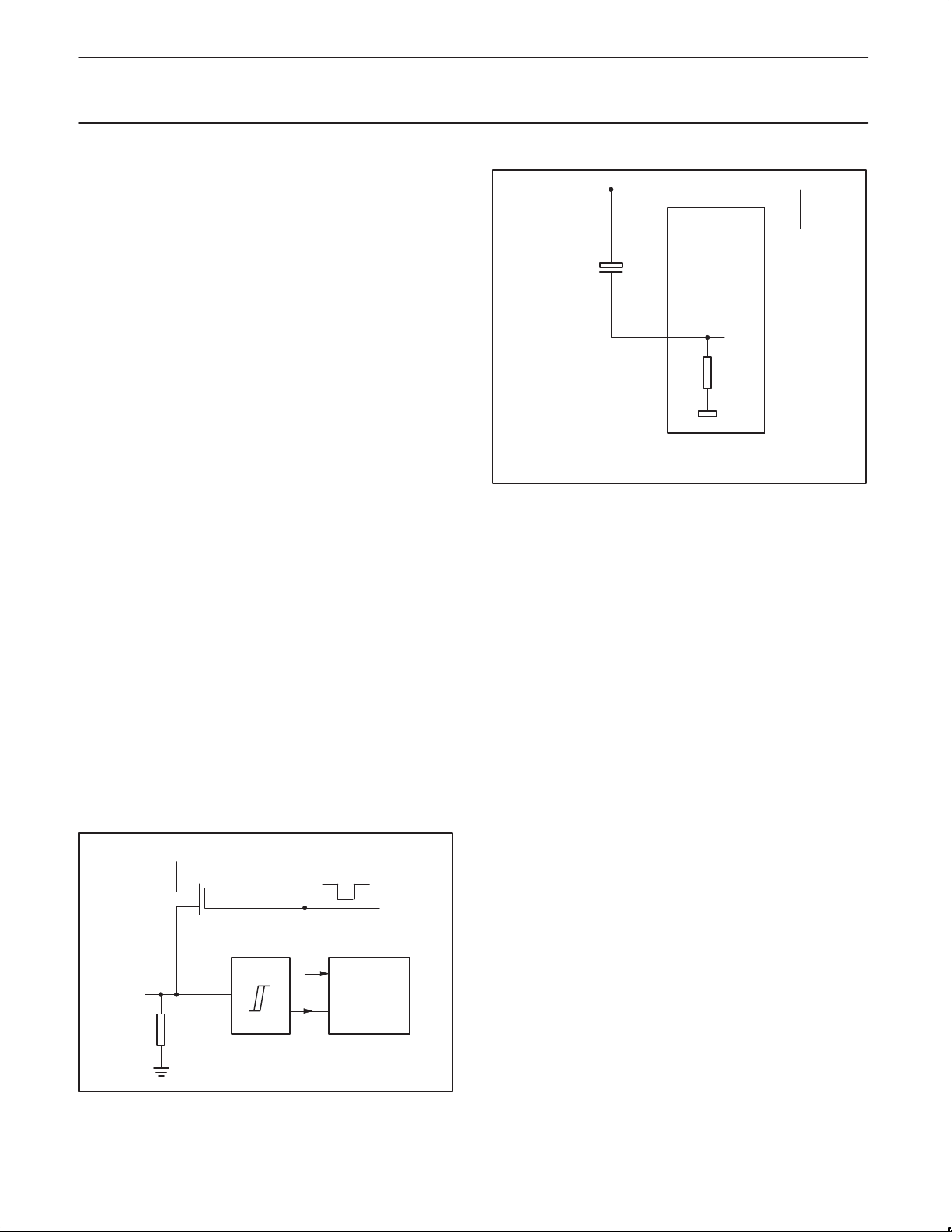
The RST line can also be pulled HIGH internally by a pull-up
transistor activated by the watchdog timer T3. The length of the
output pulse from T3 is 3 machine cycles. A pulse of such short
duration is necessary in order to recover from a processor or system
fault as fast as possible.
Note that the short reset pulse from Timer T3 cannot discharge the
power-on reset capacitor (see Figure 2). Consequently, when the
watchdog timer is also used to set external devices, this capacitor
arrangement should not be connected to the RST pin, and a
different circuit should be used to perform the power-on reset
operation. A timer T3 overflow, if enabled, will force a reset condition
to the 8XC554 by an internal connection, independent of the level of
the RST pin.
A reset may be performed in software by setting the software reset
bit, SRST (AUXR1.5).
V
DD
SCHMITT
TRIGGER
RST
ON-CHIP
RESISTOR
R
RST
RESET
CIRCUITRY
Figure 1. On-Chip Reset Configuration
and the
DD
OVERFLOW
TIMER T3
SU00952
V
DD
V
DD
2.2 µF
+
8XC554
RST
R
RST
SU00953
Figure 2. Power-On Reset
LOW POWER MODES
Stop Clock Mode
The static design enables the clock speed to be reduced down to
0 MHz (stopped). When the oscillator is stopped, the RAM and
Special Function Registers retain their values. This mode allows
step-by-step utilization and permits reduced system power
consumption by lowering the clock frequency down to any value. For
lowest power consumption the Power Down mode is suggested.
Idle Mode
In the idle mode (see Table 2), the CPU puts itself to sleep while
some of the on-chip peripherals stay active. The instruction to
invoke the idle mode is the last instruction executed in the normal
operating mode before the idle mode is activated. The CPU
contents, the on-chip RAM, and all of the special function registers
remain intact during this mode. The idle mode can be terminated
either by any enabled interrupt (at which time the process is picked
up at the interrupt service routine and continued), or by a hardware
reset which starts the processor in the same manner as a power-on
reset.
Power-Down Mode
To save even more power, a Power Down mode (see Table 2) can
be invoked by software. In this mode, the oscillator is stopped and
the instruction that invoked Power Down is the last instruction
executed. The on-chip RAM and Special Function Registers retain
their values down to 2.0V and care must be taken to return V
the minimum specified operating voltages before the Power Down
Mode is terminated.
Either a hardware reset or external interrupt can be used to exit from
Power Down. The Wake-up from Power-down bit, WUPD (AUXR1.3)
must be set in order for an external interrupt to cause a wake-up
from power-down. Reset redefines all the SFRs but does not
change the on-chip RAM. An external interrupt allows both the SFRs
and the on-chip RAM to retain their values.
To properly terminate Power Down the reset or external interrupt
should not be executed before V
is restored to its normal
CC
operating level and must be held active long enough for the
oscillator to restart and stabilize (normally less than 10ms).
CC
to
1999 Apr 07
9
Page 10

Philips Semiconductors Preliminary specification
80C51 8-bit microcontroller
16K/512 OTP/ROM/ROMless, 8 channel 10 bit A/D, I2C, PWM,
80C554/83C554/87C554
capture/compare, high I/O
Table 2. External Pin Status During Idle and Power-Down Modes
MODE
Idle Internal 1 1 Data Data Data Data Data High
Idle External 1 1 Float Data Address Data Data High
Power-down Internal 0 0 Data Data Data Data Data High
Power-down External 0 0 Float Data Data Data Data High
PROGRAM
MEMORY
ALE PSEN PORT 0 PORT 1 PORT 2 PORT 3 PORT 4
PWM0/
PWM1
With an external interrupt, INT0 and INT1 must be enabled and
configured as level-sensitive. Holding the pin low restarts the oscillator
but bringing the pin back high completes the exit. Once the interrupt
is serviced, the next instruction to be executed after RETI will be the
one following the instruction that put the device into Power Down.
POWER OFF FLAG
The Power Off Flag (POF) is set by on-chip circuitry when the V
level on the 8XC554 rises from 0 to 5V. The POF bit can be set or
cleared by software allowing a user to determine if the reset is the
result of a power-on or a warm start after powerdown. The V
must remain above 3V for the POF to remain unaffected by the V
level.
CC
CC
level
CC
Design Consideration
•When the idle mode is terminated by a hardware reset, the device
normally resumes program execution, from where it left off, up to
two machine cycles before the internal reset algorithm takes
control. On-chip hardware inhibits access to internal RAM in this
event, but access to the port pins is not inhibited. To eliminate the
possibility of an unexpected write when Idle is terminated by reset,
the instruction following the one that invokes Idle should not be
one that writes to a port pin or to external memory.
PCON
(87H)
ONCE Mode
The ONCE (“On-Circuit Emulation”) Mode facilitates testing and
debugging of systems without the device having to be removed from
the circuit. The ONCE Mode is invoked by:
1. Pull ALE low while the device is in reset and PSEN
2. Hold ALE low as RST is deactivated.
While the device is in ONCE Mode, the Port 0 pins go into a float
state, and the other port pins and ALE and PSEN
high. The oscillator circuit remains active. While the device is in this
mode, an emulator or test CPU can be used to drive the circuit.
Normal operation is restored when a normal reset is applied.
is high;
are weakly pulled
Reduced EMI Mode
The ALE-Off bit, AO (AUXR.0) can be set to disable the ALE output.
It will automatically become active when required for external
memory accesses and resume to the OFF state after completing the
external memory access.
01234567
PDGF0GF1WLEPOFSMOD0SMOD1
IDL
(LSB)(MSB)
BIT SYMBOL FUNCTION
PCON.7 SMOD1 Double Baud rate bit. When set to logic 1, the baud rate is doubled when the serial port SIO0 is being
PCON.6 SMOD0 Selects SM0/FE for SCON.7 bit.
PCON.5 POF Power Off Flag
PCON.4 WLE Watchdog Load Enable. This flag must be set by software prior to loading timer T3 (watchdog timer). It is
PCON.3 GF1 General-purpose flag bit.
PCON.2 GF0 General-purpose flag bit.
PCON.1 PD Power-down bit. Setting this bit activates the power-down mode. It can only be set if input EW
PCON.0 IDL Idle mode bit. Setting this bit activates the Idle mode.
If logic 1s are written to PD and IDL at the same time, PD takes precedence. The reset value of PCON is (00X00000).
1999 Apr 07
used in modes 1, 2, or 3.
cleared when timer T3 is loaded.
Figure 3. Power Control Register (PCON)
10
is high.
SU00954
Page 11

Philips Semiconductors Preliminary specification
80C51 8-bit microcontroller
16K/512 OTP/ROM/ROMless, 8 channel 10 bit A/D, I2C, PWM,
80C554/83C554/87C554
capture/compare, high I/O
Expanded Data RAM Addressing
The 8xC554 has internal data memory that is mapped into four
separate segments: the lower 128 bytes of RAM, upper 128 bytes of
RAM, 128 byte s S pecial Func tion Regist er (SFR), and 256 bytes
expanded RAM (EXTRAM).
The four segments are:
1. The Lower 128 bytes of RAM (addresses 00H to 7FH) are
directly and indirectly addressable.
2. The Upper 128 bytes of RAM (addresses 80H to FFH) are
indirectly addressable only.
3. The Special Function Registers, SFRs, (addresses 80H to FFH)
are directly addressable only.
4. The 256-bytes expanded RAM (ERAM, 00H – FFH) are indirectly
accessed by move external instruction, MOVX, and with the
EXTRAM bit cleared, see Figure 4.
The Lower 128 bytes can be accessed by either direct or indirect
addressing. The Upper 128 bytes can be accessed by indirect
addressing only . The Upper 128 bytes occupy the same address
space as the SFR. That means they have the same address, but are
physically separate from SFR space.
When an instruction accesses an internal location above address
7FH, the CPU knows whether the access is to the upper 128 bytes
of data RAM or to SFR space by the addressing mode used in the
instruction. Instructions that use direct addressing access SFR
space. For example:
MOV 0A0H,#data
accesses the SFR at location 0A0H (which is P2). Instructions that
use indirect addressing access the Upper 128 bytes of data RAM.
For example:
MOV @R0,#data
where R0 contains 0A0H, accesses the data byte at address 0A0H,
rather than P2 (whose address is 0A0H).
The ERAM can be accessed by indirect addressing, with EXTRAM
bit cleared and MOVX instructions. This part of memory is physically
located on-chip, logically occupies the first 256-bytes of external
data memory.
With EXTRAM = 0, the EXTRAM is indirectly addressed, using the
MOVX instruction in combination with any of the registers R0, R1 of
the selected bank or DPTR. An access to ERAM will not affect ports
P0, P3.6 (WR#) and P3.7 (RD#). P2 SFR is output during expanded
RAM addressing. For example, with EXTRAM = 0,
MOVX @R0,#data
where R0 contains 0A0H, accesses the ERAM at address 0A0H
rather than external memory. An access to external data memory
locations higher than FFH (i.e., 0100H to FFFFH) will be performed
with the MOVX DPTR instructions in the same way as in the
standard 80C51, so with P0 and P2 as data/address bus, and P3.6
and P3.7 as write and read timing signals. Refer to Figure 5.
With EXTRAM = 1, MOVX @Ri and MOVX @DPTR will be similar
to the standard 80C51. MOVX @ Ri will provide an 8-bit address
multiplexed with data on Port 0 and any output port pins can be
used to output higher order address bits. This is to provide the
external paging capability. MOVX @DPTR will generate a 16-bit
address. Port 2 outputs the high-order eight address bits (the
contents of DPH) while Port 0 multiplexes the low-order eight
address bits (DPL) with data. MOVX @Ri and MOVX @DPTR will
generate either read or write signals on P3.6 (#WR) and P3.7 (#RD).
The stack pointer (SP) may be located anywhere in the 256 bytes
RAM (lower and upper RAM) internal data memory. The stack may
not be located in the ERAM address space.
AUXR
Symbol Function
AO Disable/Enable ALE
EXTRAM Internal/External RAM (00H – FFH) access using MOVX @Ri/@DPTR
LVADC Enable A/D low voltage operation
— Not implemented, reserved for future use*.
NOTE:
*User software should not write 1s to reserved bits. These bits may be used in future 8051 family products to invoke new features. In that
case, the reset or inactive value of the new bit will be 0, and its active value will be 1. The value read from a reserved bit is indeterminate.
Address = 8EH
Not Bit Addressable
— ————LVADC EXTRAM AO
Bit:
AO Operating Mode
0 ALE is emitted at a constant rate of 1/6 the oscillator frequency.
1 ALE is active only during a MOVX or MOVC instruction.
EXTRAM Operating Mode
0 Internal ERAM (00H–FFH) access using MOVX @Ri/@DPTR
1 External data memory access.
LVADC Operating Mode
0 Turns off A/D charge pump.
1 T urns on A/D charge pump. Required for operation below 4V.
76543210
Figure 4. AUXR: Auxiliary Register
Reset Value = xxxx x110B
SU00979A
1999 Apr 07
11
Page 12

Philips Semiconductors Preliminary specification
80C51 8-bit microcontroller
16K/512 OTP/ROM/ROMless, 8 channel 10 bit A/D, I2C, PWM,
80C554/83C554/87C554
capture/compare, high I/O
FF
ERAM
256 BYTES
00
FF
UPPER
128 BYTES
INTERNAL RAM
80 80
LOWER
128 BYTES
INTERNAL RAM
00
Figure 5. Internal and External Data Memory Address Space with EXTRAM = 0
Dual DPTR
The dual DPTR structure (see Figure 6) is a way by which the chip
will specify the address of an external data memory location. There
are two 16-bit DPTR registers that address the external memory,
and a single bit called DPS = AUXR1/bit0 that allows the program
code to switch between them.
The DPS bit status should be saved by software when switching
between DPTR0 and DPTR1.
DPS
BIT0
AUXR1
DPH
(83H)
DPL
(82H)
Figure 6.
DPTR1
DPTR0
EXTERNAL
DATA
MEMORY
SU00745A
FF
SPECIAL
FUNCTION
REGISTER
00
FFFF
0100
0000
EXTERNAL
DATA
MEMORY
SU00980
Note that bit 2 is not writable and is always read as a zero. This
allows the DPS bit to be quickly toggled simply by executing an
INC AUXR1 instruction without affecting the other bits.
DPTR Instructions
The instructions that refer to DPTR refer to the data pointer that is
currently selected using the AUXR1/bit 0 register. The six
instructions that use the DPTR are as follows:
INC DPTR Increments the data pointer by 1
MOV DPTR, #data16 Loads the DPTR with a 16-bit constant
MOV A, @ A+DPTR Move code byte relative to DPTR to ACC
MOVX A, @ DPTR Move external RAM (16-bit address) to
ACC
MOVX @ DPTR , A Move ACC to external RAM (16-bit
address)
JMP @ A + DPTR Jump indirect relative to DPTR
The data pointer can be accessed on a byte-by-byte basis by
specifying the low or high byte in an instruction which accesses the
SFRs. See application note AN458 for more details.
1999 Apr 07
12
Page 13

Philips Semiconductors Preliminary specification
80C51 8-bit microcontroller
16K/512 OTP/ROM/ROMless, 8 channel 10 bit A/D, I2C, PWM,
80C554/83C554/87C554
capture/compare, high I/O
AUXR1
Symbol Function
DPS Data Pointer Switch—switches between DPRT0 and DPTR1.
WUPD Enable wakeup from powerdown.
GF2 General Purpose Flag—set and cleared by the user.
SRST Software Reset
AIDL Enables the ADC during idle mode.
ADC8 ADC Mode Switch—switches between 10-bit conversion and 8-bit conversion.
NOTE:
*User software should not write 1s to reserved bits. These bits may be used in future 8051 family products to invoke new features. In that
case, the reset or inactive value of the new bit will be 0, and its active value will be 1. The value read from a reserved bit is indeterminate.
Address = A2H
Not Bit Addressable
ADC8 AIDL SRST GF2 WUPD 0 — DSP
Bit:
DPS Operating Mode
0 DPTR0
1 DPTR1
ADC8 Operating Mode
0 10-bit conversion (50 machine cycles)
1 8-bit conversion (24 machine cycles)
76543210
Figure 7. AUXR1: DPTR Control Register
Reset Value = 0000 00x0B
SU01081
1999 Apr 07
13
Page 14

Philips Semiconductors Preliminary specification
80C51 8-bit microcontroller
16K/512 OTP/ROM/ROMless, 8 channel 10 bit A/D, I2C, PWM,
80C554/83C554/87C554
capture/compare, high I/O
Enhanced UART
The UART operates in all of the usual modes that are described in
the first section of
Microcontrollers
detect by looking for missing stop bits, and automatic address
recognition. The UART also fully supports multiprocessor
communication as does the standard 80C51 UART.
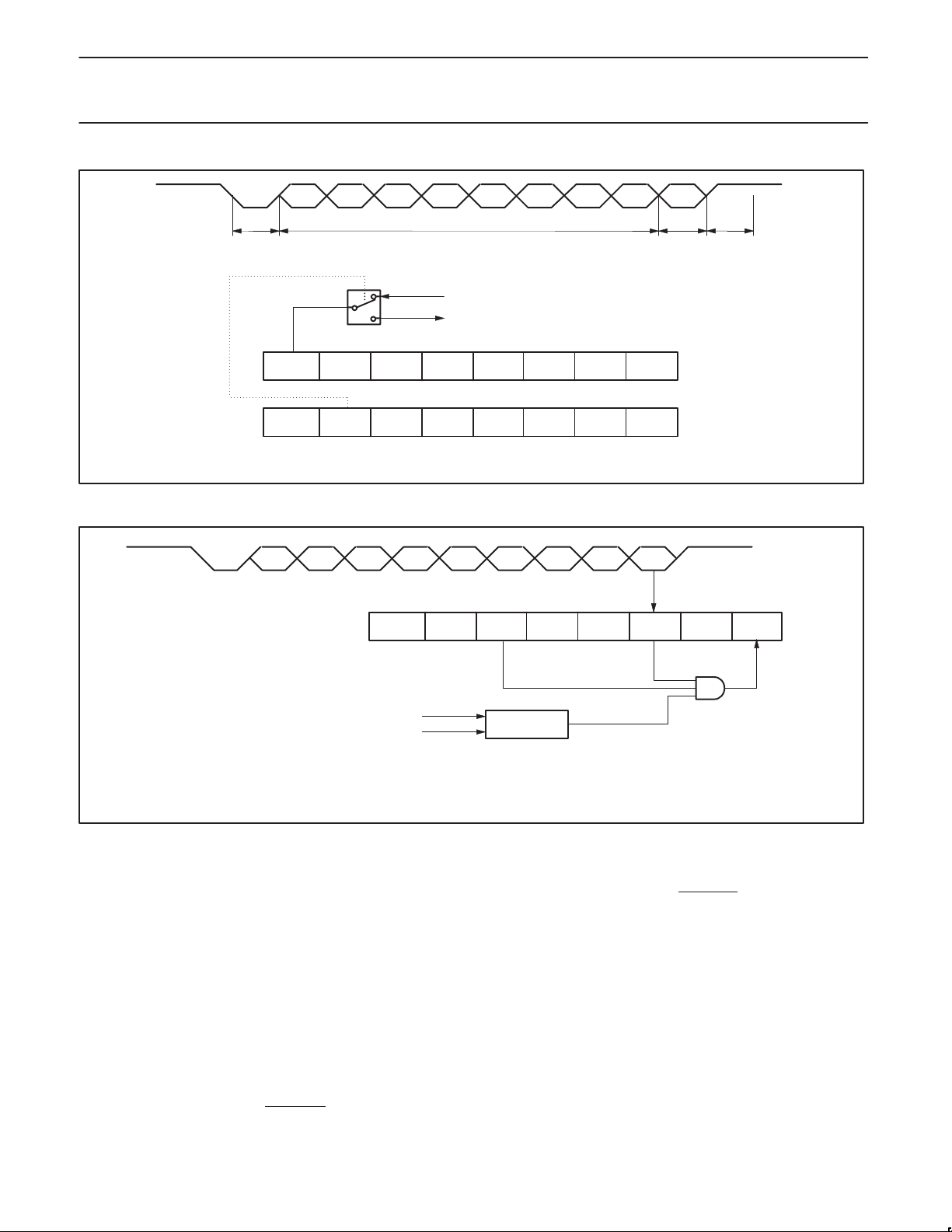
When used for framing error detect the UART looks for missing stop
bits in the communication. A missing bit will set the FE bit in the
S0CON register. The FE bit shares the S0CON.7 bit with SM0 and
the function of S0CON.7 is determined by PCON.6 (SMOD0) (see
Figure 8). If SMOD0 is set then S0CON.7 functions as FE.
S0CON.7 functions as SM0 when SMOD0 is cleared. When used as
FE S0CON.7 can only be cleared by software. Refer to Figure 9.
Automatic Address Recognition
Automatic Address Recognition is a feature which allows the UART
to recognize certain addresses in the serial bit stream by using
Symbol Function
Data Handbook IC20, 80C51-Based 8-Bit
. In addition the UART can perform framing error
S0CON Address = 98H
Bit Addressable
SM0/FE SM1 SM2 REN TB8 RB8 Tl Rl
Bit: 76543210
(SMOD0 = 0/1)*
hardware to make the comparisons. This feature saves a great deal
of software overhead by eliminating the need for the software to
examine every serial address which passes by the serial port. This
feature is enabled by setting the SM2 bit in S0CON. In the 9 bit
UART modes, mode 2 and mode 3, the Receive Interrupt flag (RI)
will be automatically set when the received byte contains either the
“Given” address or the “Broadcast” address. The 9 bit mode
requires that the 9th information bit is a 1 to indicate that the
received information is an address and not data. Automatic address
recognition is shown in Figure 10.
The 8 bit mode is called Mode 1. In this mode the RI flag will be set
if SM2 is enabled and the information received has a valid stop bit
following the 8 address bits and the information is either a Given or
Broadcast address.
Reset Value = 0000 0000B
FE Framing Error bit. This bit is set by the receiver when an invalid stop bit is detected. The FE bit is not cleared by valid
frames but should be cleared by software. The SMOD0 bit must be set to enable access to the FE bit.
SM0 Serial Port Mode Bit 0, (SMOD0 must = 0 to access bit SM0)
SM1 Serial Port Mode Bit 1
SM0 SM1 Mode Description Baud Rate**
0 0 0 shift register f
OSC
/12
0 1 1 8-bit UART variable
1 0 2 9-bit UART f
OSC
/64 or f
OSC
/32
1 1 3 9-bit UART variable
SM2 Enables the Automatic Address Recognition feature in Modes 2 or 3. If SM2 = 1 then Rl will not be set unless the
received 9th data bit (RB8) is 1, indicating an address, and the received byte is a Given or Broadcast Address.
In Mode 1, if SM2 = 1 then Rl will not be activated unless a valid stop bit was received, and the received byte is a
Given or Broadcast Address. In Mode 0, SM2 should be 0.
REN Enables serial reception. Set by software to enable reception. Clear by software to disable reception.
TB8 The 9th data bit that will be transmitted in Modes 2 and 3. Set or clear by software as desired.
RB8 In modes 2 and 3, the 9th data bit that was received. In Mode 1, if SM2 = 0, RB8 is the stop bit that was received.
In Mode 0, RB8 is not used.
Tl Transmit interrupt flag. Set by hardware at the end of the 8th bit time in Mode 0, or at the beginning of the stop bit in the
other modes, in any serial transmission. Must be cleared by software.
Rl Receive interrupt flag. Set by hardware at the end of the 8th bit time in Mode 0, or halfway through the stop bit time in
the other modes, in any serial reception (except see SM2). Must be cleared by software.
NOTE:
*SMOD0 is located at PCON6.
= oscillator frequency
**f
OSC
Figure 8. S0CON: Serial Port Control Register
SU00981
1999 Apr 07
14
Page 15
Philips Semiconductors Preliminary specification
80C51 8-bit microcontroller
16K/512 OTP/ROM/ROMless, 8 channel 10 bit A/D, I2C, PWM,
80C554/83C554/87C554
capture/compare, high I/O
D0 D1 D2 D3 D4 D5 D6 D7 D8
START
BIT
SM0 / FE SM1 SM2 REN TB8 RB8 TI RI
SMOD1 SMOD0 POF WLE GF1 GF0 PD IDL
0 : S0CON.7 = SM0
1 : S0CON.7 = FE
DATA BYTE
SET FE BIT IF STOP BIT IS 0 (FRAMING ERROR)
SM0 TO UART MODE CONTROL
Figure 9. UART Framing Error Detection
D0 D1 D2 D3 D4 D5 D6 D7 D8
SM0 SM1 SM2 REN TB8 RB8 TI RI
1
1
1
0
11 X
ONLY IN
MODE 2, 3
SCON
(98H)
PCON
(87H)
STOP
BIT
SU00982
SCON
(98H)
RECEIVED ADDRESS D0 TO D7
PROGRAMMED ADDRESS
IN UART MODE 2 OR MODE 3 AND SM2 = 1:
INTERRUPT IF REN=1, RB8=1 AND “RECEIVED ADDRESS” = “PROGRAMMED ADDRESS”
– WHEN OWN ADDRESS RECEIVED, CLEAR SM2 TO RECEIVE DATA BYTES
– WHEN ALL DATA BYTES HAVE BEEN RECEIVED: SET SM2 TO WAIT FOR NEXT ADDRESS.
Figure 10. UART Multiprocessor Communication, Automatic Address Recognition
Mode 0 is the Shift Register mode and SM2 is ignored.
Using the Automatic Address Recognition feature allows a master to
selectively communicate with one or more slaves by invoking the
Given slave address or addresses. All of the slaves may be
contacted by using the Broadcast address. Two special Function
Registers are used to define the slave’s address, SADDR, and the
address mask, SADEN. SADEN is used to define which bits in the
SADDR are to b used and which bits are “don’t care”. The SADEN
mask can be logically ANDed with the SADDR to create the “Given”
address which the master will use for addressing each of the slaves.
Use of the Given address allows multiple slaves to be recognized
while excluding others. The following examples will help to show the
versatility of this scheme:
Slave 0 SADDR = 1100 0000
SADEN = 1111 1101
Given = 1100 00X0
COMPARATOR
SU00045
Slave 1 SADDR = 1100 0000
SADEN = 1111 1110
Given = 1100 000X
In the above example SADDR is the same and the SADEN data is
used to differentiate between the two slaves. Slave 0 requires a 0 in
bit 0 and it ignores bit 1. Slave 1 requires a 0 in bit 1 and bit 0 is
ignored. A unique address for Slave 0 would be 1100 0010 since
slave 1 requires a 0 in bit 1. A unique address for slave 1 would be
1100 0001 since a 1 in bit 0 will exclude slave 0. Both slaves can be
selected at the same time by an address which has bit 0 = 0 (for
slave 0) and bit 1 = 0 (for slave 1). Thus, both could be addressed
with 1100 0000.
1999 Apr 07
15
Page 16

Philips Semiconductors Preliminary specification
80C51 8-bit microcontroller
16K/512 OTP/ROM/ROMless, 8 channel 10 bit A/D, I2C, PWM,
80C554/83C554/87C554
capture/compare, high I/O
In a more complex system the following could be used to select
slaves 1 and 2 while excluding slave 0:
Slave 0 SADDR = 1100 0000
SADEN = 1111 1001
Given = 1100 0XX0
Slave 1 SADDR = 1110 0000
Slave 2 SADDR = 1110 0000
In the above example the differentiation among the 3 slaves is in the
lower 3 address bits. Slave 0 requires that bit 0 = 0 and it can be
uniquely addressed by 1110 01 10. Slave 1 requires that bit 1 = 0 and
it can be uniquely addressed by 1110 and 0101. Slave 2 requires
that bit 2 = 0 and its unique address is 1110 0011. To select Slaves 0
and 1 and exclude Slave 2 use address 1110 0100, since it is
necessary to make bit 2 = 1 to exclude slave 2.
The Broadcast Address for each slave is created by taking the
logical OR of SADDR and SADEN. Zeros in this result are trended
as don’t-cares. In most cases, interpreting the don’t-cares as ones,
the broadcast address will be FF hexadecimal.
Upon reset SADDR (SFR address 0A9H) and SADEN (SFR
address 0B9H) are leaded with 0s. This produces a given address
of all “don’t cares” as well as a Broadcast address of all “don’t
cares”. This effectively disables the Automatic Addressing mode and
allows the microcontroller to use standard 80C51 type UART drivers
which do not make use of this feature.
Timer T2
Timer T2 is a 16-bit timer consisting of two registers TMH2 (HIGH
byte) and TML2 (LOW byte). The 16-bit timer/counter can be
switched off or clocked via a prescaler from one of two sources:
f
/12 or an external signal. When Timer T2 is configured as a
OSC
counter, the prescaler is clocked by an external signal on T2 (P1.4).
A rising edge on T2 increments the prescaler, and the maximum
repetition rate is one count per machine cycle (1MHz with a 12MHz
oscillator).
The maximum repetition rate for Timer T2 is twice the maximum
repetition rate for Timer 0 and Timer 1. T2 (P1.4) is sampled at
S2P1 and again at S5P1 (i.e., twice per machine cycle). A rising
edge is detected when T2 is LOW during one sample and HIGH
during the next sample. To ensure that a rising edge is detected, the
input signal must be LOW for at least 1/2 cycle and then HIGH for at
least 1/2 cycle. If a rising edge is detected before the end of S2P1,
the timer will be incremented during the following cycle; otherwise it
will be incremented one cycle later. The prescaler has a
programmable division factor of 1, 2, 4, or 8 and is cleared if its
division factor or input source is changed, or if the timer/counter is
reset.
Timer T2 may be read “on the fly” but possesses no extra read
latches, and software precautions may have to be taken to avoid
misinterpretation in the event of an overflow from least to most
significant byte while Timer T2 is being read. Timer T2 is not
loadable and is reset by the RST signal or by a rising edge on the
input signal RT2, if enabled. RT2 is enabled by setting bit T2ER
(TM2CON.5).
When the least significant byte of the timer overflows or when a
16-bit overflow occurs, an interrupt request may be generated.
SADEN = 1111 1010
Given = 11 10 0X0X
SADEN = 1111 1100
Given = 1110 00XX
Either or both of these overflows can be programmed to request an
interrupt. In both cases, the interrupt vector will be the same. When
the lower byte (TML2) overflows, flag T2B0 (TM2CON) is set and
flag T20V (TM2IR) is set when TMH2 overflows. These flags are set
one cycle after an overflow occurs. Note that when T20V is set,
T2B0 will also be set. To enable the byte overflow interrupt, bits ET2
(IEN1.7, enable overflow interrupt, see Figure 11) and T2IS0
(TM2CON.6, byte overflow interrupt select) must be set. Bit TWB0
(TM2CON.4) is the Timer T2 byte overflow flag.
To enable the 16-bit overflow interrupt, bits ET2 (IE1.7, enable
overflow interrupt) and T2IS1 (TM2CON.7, 16-bit overflow interrupt
select) must be set. Bit T2OV (TM2IR.7) is the Timer T2 16-bit
overflow flag. All interrupt flags must be reset by software. To enable
both byte and 16-bit overflow, T2IS0 and T2IS1 must be set and two
interrupt service routines are required. A test on the overflow flags
indicates which routine must be executed. For each routine, only the
corresponding overflow flag must be cleared.
Timer T2 may be reset by a rising edge on RT2 (P1.5) if the Timer
T2 external reset enable bit (T2ER) in T2CON is set. This reset also
clears the prescaler. In the idle mode, the timer/counter and
prescaler are reset and halted. Timer T2 is controlled by the
TM2CON special function register (see Figure 12).
Timer T2 Extension: When a 12MHz oscillator is used, a 16-bit
overflow on Timer T2 occurs every 65.5, 131, 262, or 524 ms,
depending on the prescaler division ratio; i.e., the maximum cycle
time is approximately 0.5 seconds. In applications where cycle times
are greater than 0.5 seconds, it is necessary to extend Timer T2.
This is achieved by selecting fosc/12 as the clock source (set
T2MS0, reset T2MS1), setting the prescaler division ration to 1/8
(set T2P0, set T2P1), disabling the byte overflow interrupt (reset
T2IS0) and enabling the 16-bit overflow interrupt (set T2IS1). The
following software routine is written for a three-byte extension which
gives a maximum cycle time of approximately 2400 hours.
OVINT: PUSH ACC ;save accumulator
PUSH PSW ;save status
INC TIMEX1 ;increment first byte (low order)
;of extended timer
MOV A,TIMEX1
JNZ INTEX ;jump to INTEX if ;there is no overflow
INC TIMEX2 ;increment second byte
MOV A,TIMEX2
JNZ INTEX ;jump to INTEX if there is no overflow
INC TIMEX3 ;increment third byte (high order)
INTEX: CLR T2OV ;reset interrupt flag
POP PSW ;restore status
POP ACC ;restore accumulator
RETI ;return from interrupt
Timer T2, Capture and Compare Logic: Timer T2 is connected to
four 16-bit capture registers and three 16-bit compare registers. A
capture register may be used to capture the contents of Timer T2
when a transition occurs on its corresponding input pin. A compare
register may be used to set, reset, or toggle port 4 output pins at
certain pre-programmable time intervals.
The combination of Timer T2 and the capture and compare logic is
very powerful in applications involving rotating machinery,
automotive injection systems, etc. Timer T2 and the capture and
compare logic are shown in Figure 13.
1999 Apr 07
16
Page 17

Philips Semiconductors Preliminary specification
80C51 8-bit microcontroller
16K/512 OTP/ROM/ROMless, 8 channel 10 bit A/D, I2C, PWM,
80C554/83C554/87C554
capture/compare, high I/O
IEN1 (E8H)
TM2CON (EAH)
01234567
ECT1ECT2ECT3ECM0ECM1ECM2ET2
BIT SYMBOL FUNCTION
IEN1.7 ET2 Enable Timer T2 overflow interrupt(s)
IEN1.6 ECM2 Enable T2 Comparator 2 interrupt
IEN1.5 ECM1 Enable T2 Comparator 1 interrupt
IEN1.4 ECM0 Enable T2 Comparator 0 interrupt
IEN1.3 ECT3 Enable T2 Capture register 3 interrupt
IEN1.2 ECT2 Enable T2 Capture register 2 interrupt
IEN1.1 ECT1 Enable T2 Capture register 1 interrupt
IEN1.0 ECT0 Enable T2 Capture register 0 interrupt
Figure 11. Timer T2 Interrupt Enable Register (IEN1)
T2MS1T2P0T2P1T2BOT2ERT2IS0T2IS1
BIT SYMBOL FUNCTION
TM2CON.7 TSIS1 Timer T2 16-bit overflow interrupt select
TM2CON.6 T2IS0 Timer T2 byte overflow interrupt select
TM2CON.5 T2ER Timer T2 external reset enable. When this bit is set,
TM2CON.4 T2BO Timer T2 byte overflow interrupt flag
TM2CON.3 T2P1
TM2CON.2 T2P0
Timer T2 may be reset by a rising edge on RT2 (P1.5).
Timer T2 prescaler select
ECT0
(LSB)(MSB)
01234567
T2MS0
(LSB)(MSB)
Reset Value = 00H
SU01083
Reset Value = 00H
T2P1 T2P0 Timer T2 Clock
0 0 Clock source
0 1 Clock source/2
1 0 Clock source/4
1 1 Clock source/8
TM2CON.1 T2MS1
TM2CON.0 T2MS0
T2MS1 T2MS0 Mode Selected
0 0 Timer T2 halted (of f)
0 1 T2 clock source = f
1 0 Test mode; do not use
1 1 T2 clock source = pin T2
Figure 12. T2 Control Register (TM2CON)
Timer T2 mode select
OSC
/12
SU01084
1999 Apr 07
17
Page 18

Philips Semiconductors Preliminary specification
80C51 8-bit microcontroller
16K/512 OTP/ROM/ROMless, 8 channel 10 bit A/D, I2C, PWM,
80C554/83C554/87C554
capture/compare, high I/O
off
f
osc
T2
RT2
T2ER
External reset
S
S
S
S
S
S
TG
TG
STE RTE
1/12
enable
INTCT0I
CTI0
CT0 CT1 CT2 CT3
Prescaler T2 Counter
R
R
R
R
R
R
T
T
P4.0
P4.1
P4.2
P4.3
P4.4
P4.5
P4.6
P4.7
I/O port 4
CT1I
CT2I
CTI1
COMP
CMO (S)
S = set
R = reset
T = toggle
TG = toggle status
INTINT
CTI2
8-bit overflow interrupt
16-bit overflow interrupt
INT
T2 SFR address:
COMP
CM1 (R)
TML2 = lower 8 bits
TMH2 = higher 8 bits
Figure 13. Block Diagram of Timer 2
INT
CT3I
COMP
CM2 (T)
INT
CTI3
INT
SU00757
Capture Logic: The four 16-bit capture registers that Timer T2 is
connected to are: CT0, CT1, CT2, and CT3. These registers are
loaded with the contents of Timer T2, and an interrupt is requested
upon receipt of the input signals CT0I, CT1I, CT2I, or CT3I. These
input signals are shared with port 1. The four interrupt flags are in
the Timer T2 interrupt register (TM2IR special function register). If
the capture facility is not required, these inputs can be regarded as
additional external interrupt inputs.
Using the capture control register CTCON (see Figure 14), these
inputs may capture on a rising edge, a falling edge, or on either a
rising or falling edge. The inputs are sampled during S1P1 of each
cycle. When a selected edge is detected, the contents of Timer T2
are captured at the end of the cycle.
Measuring Time Intervals Using Capture Registers: When a
recurring external event is represented in the form of rising or falling
edges on one of the four capture pins, the time between two events
can be measured using Timer T2 and a capture register . When an
event occurs, the contents of Timer T2 are copied into the relevant
capture register and an interrupt request is generated. The interrupt
service routine may then compute the interval time if it knows the
previous contents of Timer T2 when the last event occurred. With a
12MHz oscillator, Timer T2 can be programmed to overflow every
524ms. When event interval times are shorter than this, computing
the interval time is simple, and the interrupt service routine is short.
For longer interval times, the Timer T2 extension routine may be
used.
Compare Logic: Each time Timer T2 is incremented, the contents
of the three 16-bit compare registers CM0, CM1, and CM2 are
compared with the new counter value of Timer T2. When a match is
found, the corresponding interrupt flag in TM2IR is set at the end of
the following cycle. When a match with CM0 occurs, the controller
sets bits 0-5 of port 4 if the corresponding bits of the set enable
register STE are at logic 1.
1999 Apr 07
18
Page 19

Philips Semiconductors Preliminary specification
80C51 8-bit microcontroller
16K/512 OTP/ROM/ROMless, 8 channel 10 bit A/D, I2C, PWM,
80C554/83C554/87C554
capture/compare, high I/O
CTCON (EBH)
BIT SYMBOL CAPTURE/INTERRUPT ON:
CTCON.7 CTN3 Capture Register 3 triggered by a falling edge on CT3I
CTCON.6 CTP3 Capture Register 3 triggered by a rising edge on CT3I
CTCON.5 CTN2 Capture Register 2 triggered by a falling edge on CT2I
CTCON.4 CTP2 Capture Register 2 triggered by a rising edge on CT2I
CTCON.3 CTN1 Capture Register 1 triggered by a falling edge on CT1I
CTCON.2 CTP1 Capture Register 1 triggered by a rising edge on CT1I
CTCON.1 CTN0 Capture Register 0 triggered by a falling edge on CT0I
CTCON.0 CTP0 Capture Register 0 triggered by a rising edge on CT0I
Figure 14. Capture Control Register (CTCON)
When a match with CM1 occurs, the controller resets bits 0-5 of port
4 if the corresponding bits of the reset/toggle enable register RTE
are at logic 1 (see Figure 15 for RTE register function). If RTE is “0”,
then P4.n is not affected by a match between CM1 or CM2 and
Timer 2. When a match with CM2 occurs, the controller “toggles”
bits 6 and 7 of port 4 if the corresponding bits of the RTE are at
logic 1. The port latches of bits 6 and 7 are not toggled.
Two additional flip-flops store the last operation, and it is these
flip-flops that are toggled.
Thus, if the current operation is “set,” the next operation will be
“reset” even if the port latch is reset by software before the “reset”
operation occurs. The first “toggle” after a chip RESET will set the
port latch. The contents of these two flip-flops can be read at STE.6
and STE.7 (corresponding to P4.6 and P4.7, respectively). Bits
STE.6 and STE.7 are read only (see Figure 16 for STE register
function). A logic 1 indicates that the next toggle will set the port
latch; a logic 0 indicates that the next toggle will reset the port latch.
CM0, CM1, and CM2 are reset by the RST signal.
The modified port latch information appears at the port pin during
S5P1 of the cycle following the cycle in which a match occurred. If
the port is modified by software, the outputs change during S1P1 of
the following cycle. Each port 4 bit can be set or reset by software at
any time. A hardware modification resulting from a comparator
match takes precedence over a software modification in the same
cycle. When the comparator results require a “set” and a “reset” at
the same time, the port latch will be reset.
01234567
CTN1CTP1CTN1CTP2CTN2CTP3CTN3
Timer T2 Interrupt Flag Register TM2IR: Eight of the nine Timer
T2 interrupt flags are located in special function register TM2IR (see
Figure 17). The ninth flag is TM2CON.4.
The CT0I and CT1I flags are set during S4 of the cycle in which the
contents of Timer T2 are captured. CT0I is scanned by the interrupt
logic during S2, and CT1I is scanned during S3. CT2I and CT3I are
set during S6 and are scanned during S4 and S5. The associated
interrupt requests are recognized during the following cycle. If these
flags are polled, a transition at CT0I or CT1I will be recognized one
cycle before a transition on CT2I or CT3I since registers are read
during S5. The CMI0, CMI1, and CMI2 flags are set during S6 of the
cycle following a match. CMI0 is scanned by the interrupt logic
during S2; CMI1 and CMI2 are scanned during S3 and S4. A match
will be recognized by the interrupt logic (or by polling the flags) two
cycles after the match takes place.
The 16-bit overflow flag (T2OV) and the byte overflow flag (T2BO)
are set during S6 of the cycle in which the overflow occurs. These
flags are recognized by the interrupt logic during the next cycle.
Special function register IP1 (Figure 17) is used to determine the
Timer T2 interrupt priority. Setting a bit high gives that function a
high priority , and setting a bit low gives the function a low priority.
The functions controlled by the various bits of the IP1 register are
shown in Figure 17.
CTP0
(LSB)(MSB)
Reset Value = 00H
SU01085
1999 Apr 07
RTE (EFH)
01234567
RO41RP42RP43RP44RP45TP46TP47
BIT SYMBOL FUNCTION
RTE.7 TP47 If “1” then P4.7 toggles on a match between CM1 and Timer T2
RTE.6 TP46 If “1” then P4.6 toggles on a match between CM1 and Timer T2
RTE.5 RP45 If “1” then P4.5 is reset on a match between CM1 and Timer T2
RTE.4 RP44 If “1” then P4.4 is reset on a match between CM1 and Timer T2
RTE.3 RP43 If “1” then P4.3 is reset on a match between CM1 and Timer T2
RTE.2 RP42 If “1” then P4.2 is reset on a match between CM1 and Timer T2
RTE.1 RP41 If “1” then P4.1 is reset on a match between CM1 and Timer T2
RTE.0 RP40 If “1” then P4.0 is reset on a match between CM1 and Timer T2
Figure 15. Reset/Toggle Enable Register (RTE)
19
RP40
(LSB)(MSB)
Reset Value = 00H
SU01086
Page 20

Philips Semiconductors Preliminary specification
80C51 8-bit microcontroller
16K/512 OTP/ROM/ROMless, 8 channel 10 bit A/D, I2C, PWM,
80C554/83C554/87C554
capture/compare, high I/O
STE (EEH)
TM2IR (C8H)
01234567
SP41SP42SP43SP44SP45TG46TG47
BIT SYMBOL FUNCTION
STE.7 TG47 Toggle flip-flops
STE.6 TG46 Toggle flip-flops
STE.5 SP45 If “1” then P4.5 is set on a match between CM0 and Timer T2
STE.4 SP44 If “1” then P4.4 is set on a match between CM0 and Timer T2
STE.3 SP43 If “1” then P4.3 is set on a match between CM0 and Timer T2
STE.2 SP42 If “1” then P4.2 is set on a match between CM0 and Timer T2
STE.1 SP41 If “1” then P4.1 is set on a match between CM0 and Timer T2
STE.0 SP40 If “1” then P4.0 is set on a match between CM0 and Timer T2
Figure 16. Set Enable Register (STE)
CTI1CTI2CTI3CMI0CMI1CMI2T2OV
BIT SYMBOL FUNCTION
TM2IR.7 T2OV Timer T2 16-bit overflow interrupt flag
TM2IR.6 CMI2 CM2 interrupt flag
TM2IR.5 CMI1 CM1 interrupt flag
TM2IR.4 CMI0 CM0 interrupt flag
TM2IR.3 CTI3 CT3 interrupt flag
TM2IR.2 CTI2 CT2 interrupt flag
TM2IR.1 CTI1 CT1 interrupt flag
TM2IR.0 CTI0 CT0 interrupt flag
SP40
(LSB)(MSB)
01234567
CTI0
(LSB)(MSB)
Reset Value = C0H
SU01087
Reset Value = 00H
Interrupt Flag Register (TM2IR)
01234567
IP1 (F8H)
BIT SYMBOL FUNCTION
IP1.7 PT2 Timer T2 overflow interrupt(s) priority level
IP1.6 PCM2 T imer T2 comparator 2 interrupt priority level
IP1.5 PCM1 T imer T2 comparator 1 interrupt priority level
IP1.4 PCM0 T imer T2 comparator 0 interrupt priority level
IP1.3 PCT3 Timer T2 capture register 3 interrupt priority level
IP1.2 PCT2 Timer T2 capture register 2 interrupt priority level
IP1.1 PCT1 Timer T2 capture register 1 interrupt priority level
IP1.0 PCT0 Timer T2 capture register 0 interrupt priority level
Timer 2 Interrupt Priority Register (IP1)
Figure 17. Interrupt Flag Register (TM2IR) and Timer T2 Interrupt Priority Register (IP1)
PCT1PCT2PCT3PCM0PCM1PCM2PT2
PCT0
(LSB)(MSB)
Reset Value = 00H
SU01088
1999 Apr 07
20
Page 21

Philips Semiconductors Preliminary specification
80C51 8-bit microcontroller
16K/512 OTP/ROM/ROMless, 8 channel 10 bit A/D, I2C, PWM,
80C554/83C554/87C554
capture/compare, high I/O
Timer T3, The Watchdog T imer
In addition to Timer T2 and the standard timers, a watchdog timer is
also incorporated on the 8xC554. The purpose of a watchdog timer
is to reset the microcontroller if it enters erroneous processor states
(possibly caused by electrical noise or RFI) within a reasonable
period of time. An analogy is the “dead man’s handle” in railway
locomotives. When enabled, the watchdog circuitry will generate a
system reset if the user program fails to reload the watchdog timer
within a specified length of time known as the “watchdog interval.”
Watchdog Circuit Description: The watchdog timer (Timer T3)
consists of an 8-bit timer with an 11-bit prescaler as shown in
Figure 18. The prescaler is fed with a signal whose frequency is
1/12 the oscillator frequency (1MHz with a 12MHz oscillator). The
8-bit timer is incremented every “t” seconds, where:
t = 12 × 2048 × 1/f
(= 1.5ms at f
OSC
OSC
= 16MHz; = 1ms at f
= 24MHz)
OSC
If the 8-bit timer overflows, a short internal reset pulse is generated
which will reset the 8xC554. A short output reset pulse is also
generated at the RST pin. This short output pulse (3 machine
cycles) may be destroyed if the RST pin is connected to a capacitor.
This would not, however, affect the internal reset operation.
Watchdog operation is activated when external pin EW
When EW
is tied low, it is impossible to disable the watchdog
is tied low.
operation by software.
How to Operate the Watchdog Timer: The watchdog timer has to
be reloaded within periods that are shorter than the programmed
watchdog interval; otherwise the watchdog timer will overflow and a
system reset will be generated. The user program must therefore
continually execute sections of code which reload the watchdog
timer. The period of time elapsed between execution of these
sections of code must never exceed the watchdog interval. When
using a 16MHz oscillator, the watchdog interval is programmable
between 1.5ms and 392ms. When using a 24MHz oscillator, the
watchdog interval is programmable between 1ms and 255ms.
In order to prepare software for watchdog operation, a programmer
should first determine how long his system can sustain an
erroneous processor state. The result will be the maximum
watchdog interval. As the maximum watchdog interval becomes
shorter, it becomes more dif ficult for the programmer to ensure that
the user program always reloads the watchdog timer within the
watchdog interval, and thus it becomes more difficult to implement
watchdog operation.
The programmer must now partition the software in such a way that
reloading of the watchdog is carried out in accordance with the above
requirements. The programmer must determine the execution times
of all software modules. The effect of possible conditional branches,
subroutines, external and internal interrupts must all be taken into
account. Since it may be very difficult to evaluate the execution
times of some sections of code, the programmer should use worst
case estimations. In any event, the programmer must make sure
that the watchdog is not activated during normal operation.
The watchdog timer is reloaded in two stages in order to prevent
erroneous software from reloading the watchdog. First PCON.4
(WLE) must be set. The T3 may be loaded. When T3 is loaded,
PCON.4 (WLE) is automatically reset. T3 cannot be loaded if
PCON.4 (WLE) is reset. Reload code may be put in a subroutine as
it is called frequently. Since Timer T3 is an up-counter, a reload
value of 00H gives the maximum watchdog interval (510ms with a
12MHz oscillator), and a reload value of 0FFH gives the minimum
watchdog interval (2ms with a 12MHz oscillator).
In the idle mode, the watchdog circuitry remains active. When
watchdog operation is implemented, the power-down mode cannot
be used since both states are contradictory. Thus, when watchdog
operation is enabled by tying external pin EW
low, it is impossible to
enter the power-down mode, and an attempt to set the power-down
bit (PCON.1) will have no effect. PCON.1 will remain at logic 0.
f
OSC
1999 Apr 07
/12
EW
PRESCALER (11-BIT)
WRITE T3
CLEAR
INTERNAL BUS
TIMER T3 (8-BIT)
LOAD LOADEN
INTERNAL
RESET
CLEAR
WLE
PCON.4 PCON.1
INTERNAL BUS
Figure 18. Watchdog Timer
21
OVERFLOW
LOADEN
PD
V
DD
P
RST
R
RST
SU00955
Page 22

Philips Semiconductors Preliminary specification
80C51 8-bit microcontroller
16K/512 OTP/ROM/ROMless, 8 channel 10 bit A/D, I2C, PWM,
80C554/83C554/87C554
capture/compare, high I/O
During the early stages of software development/debugging, the
watchdog may be disabled by tying the EW
stage, EW
may be tied low to complete the debugging process.
pin high. At a later
Watchdog Software Example: The following example shows how
watchdog operation might be handled in a user program.
;at the program start:
T3 EQU 0FFH ;address of watchdog timer T3
PCON EQU 087H ;address of PCON SFR
WATCH-INTV EQU 156 ;watchdog interval (e.g., 2x100ms)
;to be inserted at each watchdog reload location within
;the user program:
LCALL WATCHDOG
;watchdog service routine:
WATCHDOG: ORL PCON,#10H ;set condition flag (PCON.4)
MOV T3,WATCH-INV ;load T3 with watchdog interval
RET
If it is possible for this subroutine to be called in an erroneous state,
then the condition flag WLE should be set at different parts of the
main program.
Serial I/O
The 8xC554 is equipped with two independent serial ports: SIO0
and SIO1. SIO0 is a full duplex UART port and is similar to the
Enhanced UART serial port. SIO1 accommodates the I
2
C bus.
SIO0: SIO0 is a full duplex serial I/O port identical to that of the
Enhanced UART except Time 2 cannot be used as a baud rate
generator. Its operation is the same, including the use of timer 1 as a
baud rate generator.
Port 5 Operation
Port 5 may be used to input up to 8 analog signals to the ADC.
Unused ADC inputs may be used to input digital inputs. These
inputs have an inherent hysteresis to prevent the input logic from
drawing excessive current from the power lines when driven by
analog signals. Channel to channel crosstalk (Ct) should be taken
into consideration when both analog and digital signals are
simultaneously input to Port 5 (see, D.C. characteristics in data
sheet).
Port 5 is not bidirectional and may not be configured as an output
port. All six ports are multifunctional, and their alternate functions
are listed in the Pin Descriptions section of this datasheet.
Pulse Width Modulated Outputs
The 8xC554 contains two pulse width modulated output channels
(see Figure 19). These channels generate pulses of programmable
length and interval. The repetition frequency is defined by an 8-bit
prescaler PWMP, which supplies the clock for the counter. The
prescaler and counter are common to both PWM channels. The 8-bit
counter counts modulo 255, i.e., from 0 to 254 inclusive. The value
of the 8-bit counter is compared to the contents of two registers:
PWM0 and PWM1. Provided the contents of either of these registers
is greater than the counter value, the corresponding PWM0
PWM1
output is set LOW. If the contents of these registers are
or
equal to, or less than the counter value, the output will be HIGH. The
pulse-width-ratio is therefore defined by the contents of the registers
PWM0 and PWM1. The pulse-width-ratio is in the range of 0 to 1
and may be programmed in increments of 1/255.
Buffered PWM outputs may be used to drive DC motors. The
rotation speed of the motor would be proportional to the contents of
PWMn. The PWM outputs may also be configured as a dual DAC. In
this application, the PWM outputs must be integrated using
conventional operational amplifier circuitry. If the resulting output
voltages have to be accurate, external buffers with their own analog
supply should be used to buffer the PWM outputs before they are
integrated. The repetition frequency f
, at the PWMn outputs is
PWM
give by:
f
f
PWM
2 (1 PWMP) 255
This gives a repetition frequency range of 123Hz to 31.4kHz (f
OSC
OSC
=
16MHz). At fosc = 24MHz, the frequency range is 184Hz to 47.1Hz.
By loading the PWM registers with either 00H or FFH, the PWM
channels will output a constant HIGH or LOW level, respectively.
Since the 8-bit counter counts modulo 255, it can never actually
reach the value of the PWM registers when they are loaded with
FFH.
When a compare register (PWM0 or PWM1) is loaded with a new
value, the associated output is updated immediately. It does not
have to wait until the end of the current counter period. Both PWMn
output pins are driven by push-pull drivers. These pins are not used
for any other purpose.
Prescaler frequency control register PWMP Reset Value = 00H
PWMP (FEH) 765 43210
MSB LSB
PWMP.0-7 Prescaler division factor = PWMP + 1.
Reading PWMP gives the current reload value. The actual count of
the prescaler cannot be read.
Reset Value = 00H
PWM0 (FCH)
PWM1 (FDH)
PWM0/1.0-7} Low/high ratio of PWMn
765 43 210
MSB LSB
(PWMn)
255 (PWMn)
Analog-to-Digital Converter
The analog input circuitry consists of an 8-input analog multiplexer
and a 10-bit, straight binary, successive approximation ADC. The
A/D can also be operated in 8-bit mode with faster conversion times
by setting bit ADC8 (AUXR1.7). The 8-bit results will be contained in
the ADCH register. The analog reference voltage and analog power
supplies are connected via separate input pins. For 10-bit accuracy,
the conversion takes 50 machine cycles, i.e., 37.5µs at an oscillator
frequency of 16MHz, 25µs at an oscillator frequency of 24MHz. For
the 8-bit mode, the conversion takes 24 machine cycles. Input
voltage swing is from 0V to +5V . Because the internal DAC employs
a ratiometric potentiometer , there are no discontinuities in the
converter characteristic. Figure 20 shows a functional diagram of the
analog input circuitry.
The ADC has the option of either being powered off in idle mode for
reduced power consumption or being active in idle mode for
reducing internal noise during the conversion. This option is selected
by the AIDL bit of AUXR1 register (AUXR1.6). With the AIDL bit set,
the ADC is active in the idle mode, and with the AIDL bit cleared, the
ADC is powered off in idle mode.
1999 Apr 07
22
Page 23

Philips Semiconductors Preliminary specification
80C51 8-bit microcontroller
16K/512 OTP/ROM/ROMless, 8 channel 10 bit A/D, I2C, PWM,
80C554/83C554/87C554
capture/compare, high I/O
PWM0
ADC0
ADC1
ADC2
ADC3
ADC4
ADC5
ADC6
ADC7
INTERNAL BUS
MULTIPLEXER
8-BIT COMPARATOR
f
OSC
PRESCALER1/2
PWMP
8-BIT COUNTER
8-BIT COMPARATOR
PWM1
Figure 19. Functional Diagram of Pulse Width Modulated Outputs
10-BIT A/D CONVERTERANALOG INPUT
OUTPUT
BUFFER
OUTPUT
BUFFER
PWM0
PWM1
SU00956
STADC
+
ANALOG REF.
–
ANALOG SUPPLY
ANALOG GROUND
ADCON ADCH
01234567 01234567
INTERNAL BUS
Figure 20. Functional Diagram of Analog Input Circuitry
10-Bit Analog-to-Digital Conversion: Figure 21 shows the
elements of a successive approximation (SA) ADC. The ADC
contains a DAC which converts the contents of a successive
approximation register to a voltage (VDAC) which is compared to
the analog input voltage (Vin). The output of the comparator is fed to
the successive approximation control logic which controls the
successive approximation register. A conversion is initiated by
setting ADCS in the ADCON register. ADCS can be set by software
only or by either hardware or software.
1999 Apr 07
SU00957
The software only start mode is selected when control bit ADCON.5
(ADEX) = 0. A conversion is then started by setting control bit
ADCON.3 (ADCS). The hardware or software start mode is selected
when ADCON.5 = 1, and a conversion may be started by setting
ADCON.3 as above or by applying a rising edge to external pin
STADC. When a conversion is started by applying a rising edge, a
low level must be applied to STADC for at least one machine cycle
followed by a high level for at least one machine cycle.
23
Page 24

Philips Semiconductors Preliminary specification
80C51 8-bit microcontroller
16K/512 OTP/ROM/ROMless, 8 channel 10 bit A/D, I2C, PWM,
80C554/83C554/87C554
capture/compare, high I/O
V
V
FULL SCALE 1
V
DAC
in
DAC
V
+
–
DAC
in
1/2
0
3/4
1
23456
APPROXIMATION
7/8
Figure 21. Successive Approximation ADC
The low-to-high transition of STADC is recognized at the end of a
machine cycle, and the conversion commences at the beginning of
the next cycle. When a conversion is initiated by software, the
conversion starts at the beginning of the machine cycle which
follows the instruction that sets ADCS. ADCS is actually
implemented with two flip-flops: a command flip-flop which is
affected by set operations, and a status flag which is accessed
during read operations.
The next two machine cycles are used to initiate the converter. At
the end of the first cycle, the ADCS status flag is set and a value of
“1” will be returned if the ADCS flag is read while the conversion is in
progress. Sampling of the analog input commences at the end of the
second cycle.
During the next eight machine cycles, the voltage at the previously
selected pin of port 5 is sampled, and this input voltage should be
stable in order to obtain a useful sample. In any event, the input
voltage slew rate must be less than 10V/ms in order to prevent an
undefined result.
The successive approximation control logic first sets the most
significant bit and clears all other bits in the successive
approximation register (10 0000 0000B). The output of the DAC
(50% full scale) is compared to the input voltage Vin. If the input
voltage is greater than VDAC, then the bit remains set; otherwise it
is cleared.
The successive approximation control logic now sets the next most
significant bit (11 0000 0000B or 01 0000 0000B, depending on the
t/tau
SUCCESSIVE
APPROXIMATION
CONTROL LOGIC
59/64
SU00958
SUCCESSIVE
REGISTER
START STOP
15/16
29/32
previous result), and VDAC is compared to Vin again. If the input
voltage is greater than VDAC, then the bit being tested remains set;
otherwise the bit being tested is cleared. This process is repeated
until all ten bits have been tested, at which stage the result of the
conversion is held in the successive approximation register.
Figure 22 shows a conversion flow chart. The bit pointer identifies
the bit under test. The conversion takes four machine cycles per bit.
The end of the 10-bit conversion is flagged by control bit ADCON.4
(ADCI). The upper 8 bits of the result are held in special function
register ADCH, and the two remaining bits are held in ADCON.7
(ADC.1) and ADCON.6 (ADC.0). The user may ignore the two least
significant bits in ADCON and use the ADC as an 8-bit converter (8
upper bits in ADCH). In any event, the total actual conversion time is
50 machine cycles for the 8XC552 or 24 machine cycles for the
8XC562. ADCI will be set and the ADCS status flag will be reset 50
(or 24) cycles after the command flip-flop (ADCS) is set.
Control bits ADCON.0, ADCON.1, and ADCON.2 are used to control
an analog multiplexer which selects one of eight analog channels
(see Figure 23). An ADC conversion in progress is unaffected by an
external or software ADC start. The result of a completed
conversion remains unaffected provided ADCI = logic 1; a new ADC
conversion already in progress is aborted when the idle or
power-down mode is entered. The result of a completed conversion
(ADCI = logic 1) remains unaffected when entering the idle mode.
1999 Apr 07
24
Page 25
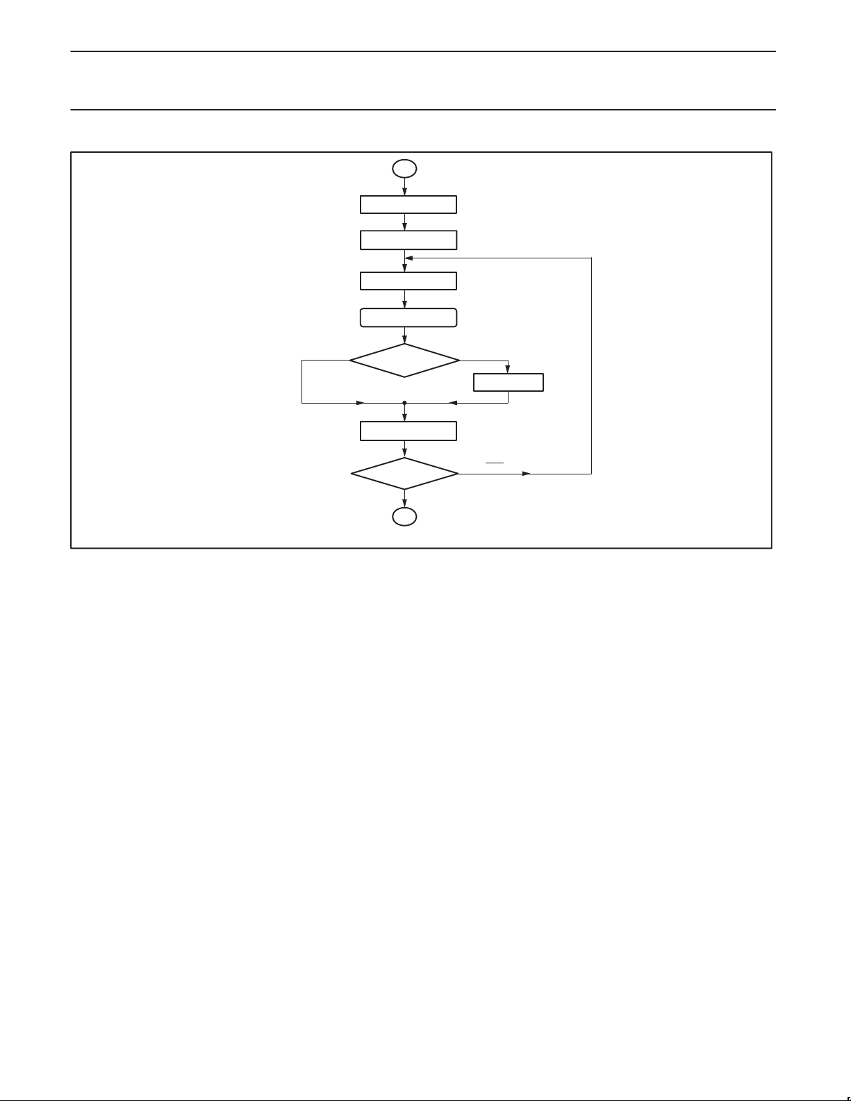
Philips Semiconductors Preliminary specification
80C51 8-bit microcontroller
16K/512 OTP/ROM/ROMless, 8 channel 10 bit A/D, I2C, PWM,
80C554/83C554/87C554
capture/compare, high I/O
Start of Conversion
SOC
RESET SAR
[BIT POINTER] = MSB
[BIT]N = 1
CONVERSION TIME
10
TEST
COMPLETE
[BIT POINTER] + 1
TEST BIT
POINTER
END
END OF CONVERSION
EOC
[BIT]N = 0
END
SU00959
Figure 22. A/D Conversion Flowchart
1999 Apr 07
25
Page 26

Philips Semiconductors Preliminary specification
80C51 8-bit microcontroller
16K/512 OTP/ROM/ROMless, 8 channel 10 bit A/D, I2C, PWM,
80C554/83C554/87C554
capture/compare, high I/O
7654321 0
ADCON (C5H)
(MSB) (LSB)
Bit Symbol Function
ADCON.7 ADC.1 Bit 1 of ADC result
ADCON.6 ADC.0
ADCON.5 ADEX
ADCON.4 ADCI
ADCON.3 ADCS
ADCON.2 AADR2
ADCON.1 AADR1
ADCON.0 AADR0
Bit 0 of ADC result
Enable external start of conversion by STADC
0 = Conversion can be started by software only (by setting ADCS)
1 = Conversion can be started by software or externally (by a rising edge on STADC)
ADC interrupt flag: this flag is set when an A/D conversion result is ready to be read. An interrupt is
invoked if it is enabled. The flag may be cleared by the interrupt service routine. While this flag is set,
the ADC cannot start a new conversion. ADCI cannot be set by software.
ADC start and status: setting this bit starts an A/D conversion. It may be set by software or by the
external signal STADC. The ADC logic ensures that this signal is HIGH while the ADC is busy. On
completion of the conversion, ADCS is reset immediately after the interrupt flag has been set. ADCS
cannot be reset by software. A new conversion may not be started while either ADCS or ADCI is high.
ADCI ADCS ADC Status
0 0 ADC not busy; a conversion can be started
0 1 ADC busy; start of a new conversion is blocked
1 0 Conversion completed; start of a new conversion requires ADCI=0
1 1 Conversion completed; start of a new conversion requires ADCI=0
If ADCI is cleared by software while ADCS is set at the same time, a new A/D conversion with the
same channel number may be started.
But it is recommended to reset ADCI
Analogue input select: this binary coded address selects one of the
eight analogue port bits of P5 to be input to the converter. It can only
be changed when ADCI and ADCS are both LOW.
AADR2 AADR1 Selected Analog Channel
0 0 ADC0 (P5.0)
0 0 ADC1 (P5.1)
0 1 ADC2 (P5.2)0
0 1 ADC3 (P5.3)1
1 0 ADC4 (P5.4)0
1 0 ADC5 (P5.5)1
1 1 ADC6 (P5.6)0
1 1 ADC7 (P5.7)1
ADEX ADCI ADCSADC.1 ADC.0
before
AADR0
0
1
Figure 23. ADC Control Register (ADCON)
AADR2 AADR1 AADR0
ADCS is set.
Reset Value = xx00 0000B
SU00960
1999 Apr 07
26
Page 27
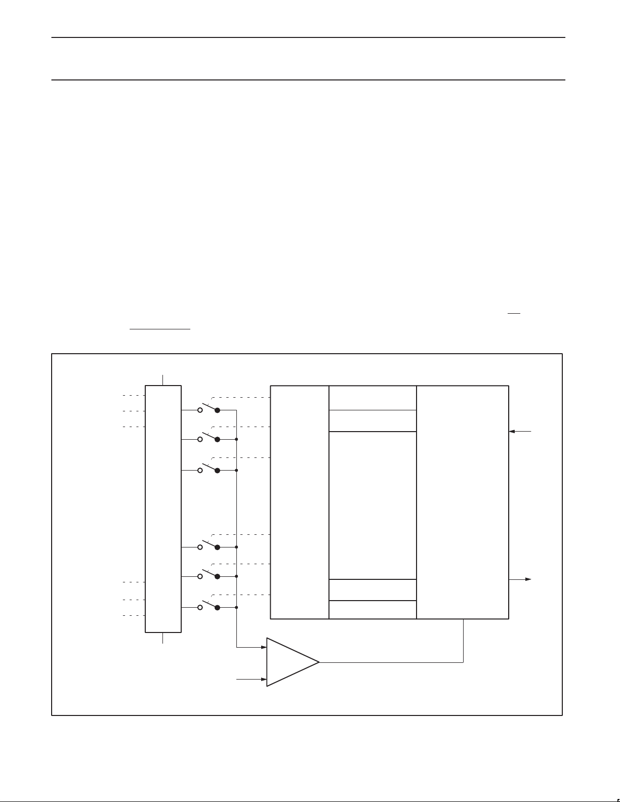
Philips Semiconductors Preliminary specification
80C51 8-bit microcontroller
16K/512 OTP/ROM/ROMless, 8 channel 10 bit A/D, I2C, PWM,
80C554/83C554/87C554
capture/compare, high I/O
10-Bit ADC Resolution and Analog Supply: Figure 24 shows how
the ADC is realized. The ADC has its own supply pins (AV
AV
) and two pins (Vref+ and Vref–) connected to each end of the
SS
DD
and
DAC’s resistance-ladder . The ladder has 1023 equally spaced taps,
separated by a resistance of “R”. The first tap is located 0.5 x R
above Vref–, and the last tap is located 1.5 x R below Vref+. This
gives a total ladder resistance of 1024 x R. This structure ensures
that the DAC is monotonic and results in a symmetrical quantization
error as shown in Figure 26.
For input voltages between Vref– and (Vref–) + 1/2 LSB, the 10-bit
result of an A/D conversion will be 00 0000 0000B = 000H. For input
voltages between (Vref+) – 3/2 LSB and V ref+, the result of a
conversion will be 11 11 11 1 111B = 3FFH. AVref+ and AVref– may
be between AV
+ 0.2V and AVSS – 0.2V. AVref+ should be
DD
positive with respect to AVref–, and the input voltage (Vin) should be
between AVref+ and AV ref–. If the analog input voltage range is from
2V to 4V , then 10-bit resolution can be obtained over this range if
AVref+ = 4V and AVref– = 2V.
The result can always be calculated from the following formula:
V
AV
IN
Result 1024
AV
R/2
R
R
R
ref
AV
AV
ref+
ref
ref
1023
1022
Power Reduction Modes
The 8XC554 has two reduced power modes of operation: the idle
mode and the power-down mode. These modes are entered by
setting bits in the PCON special function register. When the 8XC554
enters the idle mode, the following functions are disabled:
CPU (halted)
Timer T2 (halted and reset)
PWM0, PWM1 (reset; outputs are high)
ADC (may be enabled for operation in Idle mode
by setting bit AIDC (AUXR1.6) ).
In idle mode, the following functions remain active:
Timer 0
Timer 1
Timer T3
SIO0 SIO1
External interrupts
When the 8XC554 enters the power-down mode, the oscillator is
stopped. The power-down mode is entered by setting the PD bit in
the PCON register. The PD bit can only be set if the EW
input is tied
HIGH.
MSB
START
TOTAL RESISTANCE
= 1023R + 2 x R/
= 1024R
R
R
R/2
1021
DECODER
3
2
1
0
V
AV
ref–
Value 0000 0000 00 is output for voltages V
Value 111 1 1111 11 is output for voltages (V
ref
V
in
–
COMPARATOR
+
SUCCESSIVE
APPROXIMATION
REGISTER
LSB
to (V
ref–
ref–
– 3/2 LSB) to V
ref+
+ 1/2 LSB)
ref+
SUCCESSIVE
APPROXIMATION
CONTROL LOGIC
READY
SU00961
Figure 24. ADC Realization
1999 Apr 07
27
Page 28
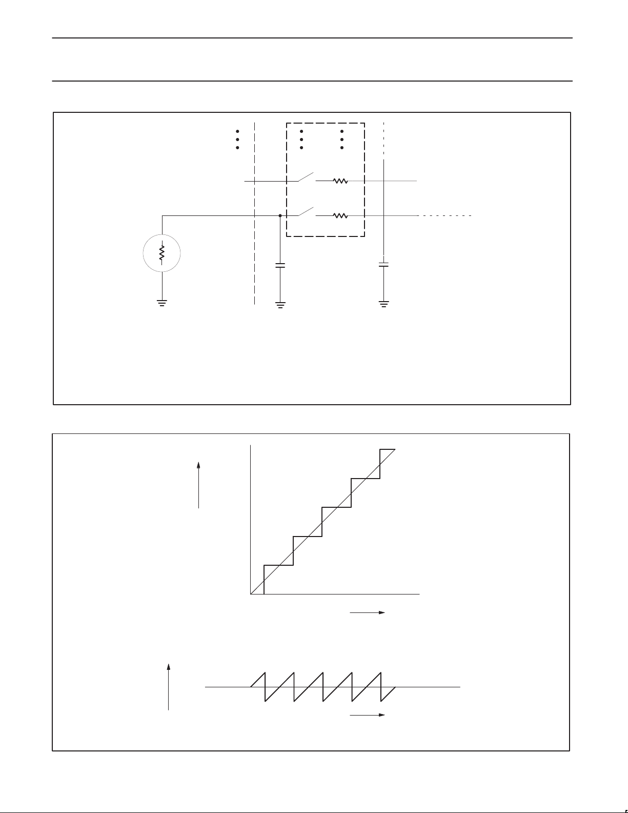
Philips Semiconductors Preliminary specification
80C51 8-bit microcontroller
16K/512 OTP/ROM/ROMless, 8 channel 10 bit A/D, I2C, PWM,
80C554/83C554/87C554
capture/compare, high I/O
I
Sm
N+1
I
N
+
R
S
V
ANALOG
INPUT
Sm
C
Rm
N+1
Rm
N
MULTIPLEXER
S
N+1
N
TO COMPARATOR
C
C
Rm = 0.5 - 3 kΩ
C
+ CC = 15pF maximum
S
= Recommended < 9.6 kΩ for 1 LSB @ 12MHz
R
S
NOTE:
Because the analog to digital converter has a sampled-data comparator, the input looks capacitive to a source. When a conversion
is initiated, switch Sm closes for 8t
be noted that the sampling causes the analog input to present a varying load to an analog source.
(8µs @ 12MHz crystal frequency) during which time capacitance CS + CC is charged. It should
CY
SU00962
Figure 25. A/D Input: Equivalent Circuit
CODE
OUT
101
Vin – V
digital
100
011
010
001
000
0 q 2q 3q 4q 5q
QUANTIZATION ERROR
q = LSB = 5 mV
+ q/2
– q/2
SYMMETRICAL QUANTIZATION ERROR
V
V
Figure 26. Effective Conversion Characteristic
in
in
SU00963
1999 Apr 07
28
Page 29

Philips Semiconductors Preliminary specification
INTERRUPT PRIORITY LEVEL
80C51 8-bit microcontroller
16K/512 OTP/ROM/ROMless, 8 channel 10 bit A/D, I2C, PWM,
80C554/83C554/87C554
capture/compare, high I/O
Interrupts
The 8XC554 has fifteen interrupt sources, each of which can be
assigned one of four priority levels. The five interrupt sources
common to the 80C51 are the external interrupts (INT0
the timer 0 and timer 1 interrupts (IT0 and IT1), and the serial I/O
interrupt (RI or TI). In the 8XC554, the standard serial interrupt is
called SIO0.
The eight Timer T2 interrupts are generated by flags CTI0-CT13,
CMI0-CMI2, and by the logical OR of flags T2OV and T2BO. Flags
CTI0 to CT13 are set by input signals CT0I to CT3i. Flags CMI0 to
CMI2 are set when a match occurs between Timer T2 and the
compare registers CM0, CM1, and CM2. When an 8-bit or 16-bit
overflow occurs, flags T2BO and T2OV are set, respectively. These
nine flags are not cleared by hardware and must be reset by
software to avoid recurring interrupts.
The ADC interrupt is generated by the ADCI flag in the ADC control
register (ADCON). This flag is set when an ADC conversion result is
ready to be read. ADCI is not cleared by hardware and must be
reset by software to avoid recurring interrupts.
The SIO1 (I
control register (S1CON). This flag is set when S1STA is loaded
with a valid status code.
The ADCI flag may be reset by software. It cannot be set by
software. All other flags that generate interrupts may be set or
cleared by software, and the effect is the same as setting or
resetting the flags by hardware. Thus, interrupts may be generated
by software and pending interrupts can be canceled by software.
Interrupt Enable Registers: Each interrupt source can be
individually enabled or disabled by setting or clearing a bit in the
2
C) interrupt is generated by the SI flag in the SIO1
and INT1),
interrupt enable special function registers IEN0 and IEN1. All
interrupt sources can also be globally enabled or disabled by setting
or clearing bit EA in IEN0. The interrupt enable registers are
described in Figures 27 and 28.
There are 3 SFRs associated with each of the four-level interrupts.
They are the IENx, IPx, and IPxH. (See Figures 29, 30, and 31.) The
IPxH (Interrupt Priority High) register makes the four-level interrupt
structure possible.
The function of the IPxH SFR is simple and when combined with the
IPx SFR determines the priority of each interrupt. The priority of
each interrupt is determined as shown in the following table:
PRIORITY BITS
IPxH.x IPx.x
0 0 Level 0 (lowest priority)
0 1 Level 1
1 0 Level 2
1 1 Level 3 (highest priority)
The priority scheme for servicing the interrupts is the same as that
for the 80C51, except there are four interrupt levels rather than two
as on the 80C51. An interrupt will be serviced as long as an interrupt
of equal or higher priority is not already being serviced. If an
interrupt of equal or higher level priority is being serviced, the new
interrupt will wait until it is finished before being serviced. If a lower
priority level interrupt is being serviced, it will be stopped and the
new interrupt serviced. When the new interrupt is finished, the lower
priority level interrupt that was stopped will be completed.
IEN0 (A8H)
BIT SYMBOL FUNCTION
IEN0.7 EA Global enable/disable control
IEN0.6 EAD Eanble ADC interrupt
IEN0.5 ES1 Enable SIO1 (I
IEN0.4 ES0 Enable SIO0 (UART) interrupt
IEN0.3 ET1 Enable Timer 1 interrupt
IEN0.2 EX1 Enable External interrupt 1
IEN0.1 ET0 Enable Timer 0 interrupt
IEN0.0 EX0 Enable External interrupt 0
Figure 27. Interrupt Enable Register (IEN0)
0 = No interrupt is enabled
1 = Any individually enabled interrupt will be accepted
2
C) interrupt
01234567
ET0EX1ET1ES0ES1EADEA
EX0
(LSB)(MSB)
SU00762
1999 Apr 07
29
Page 30

Philips Semiconductors Preliminary specification
80C51 8-bit microcontroller
16K/512 OTP/ROM/ROMless, 8 channel 10 bit A/D, I2C, PWM,
80C554/83C554/87C554
capture/compare, high I/O
01234567
IEN1 (E8H)
BIT SYMBOL FUNCTION
IEN1.7 ET2 Enable Timer T2 overflow interrupt(s)
IEN1.6 ECM2 Enable T2 Comparator 2 interrupt
IEN1.5 ECM1 Enable T2 Comparator 1 interrupt
IEN1.4 ECM0 Enable T2 Comparator 0 interrupt
IEN1.3 ECT3 Enable T2 Capture register 3 interrupt
IEN1.2 ECT2 Enable T2 Capture register 2 interrupt
IEN1.1 ECT1 Enable T2 Capture register 1 interrupt
IEN1.0 ECT0 Enable T2 Capture register 0 interrupt
In all cases, if the enable bit is 0, then the interrupt is disabled, and if the enable bit is 1, then the interrupt is enabled.
Figure 28. Interrupt Enable Register (IEN1)
ECT1ECT2ECT3ECM0ECM1ECM2ET2
ECT0
(LSB)(MSB)
SU00755
IP0 (B8H)
IP0H (B7H)
PT0PX1PT1PS0PS1PAD–
BIT SYMBOL FUNCTION
IP0.7 – Unused
IP0.6 PAD ADC interrupt priority level
IP0.5 PS1 SIO1 (I2C) interrupt priority level
IP0.4 PS0 SIO0 (UART) interrupt priority level
IP0.3 PT1 Timer 1 interrupt priority level
IP0.2 PX1 External interrupt 1 priority level
IP0.1 PT0 Timer 0 interrupt priority level
IP0.0 PX0 External interrupt 0 priority level
Figure 29. Interrupt Priority Register (IP0)
PT0HPX1HPT1HPS0HPS1HPADH–
BIT SYMBOL FUNCTION
IP0H.7 – Unused
IP0H.6 PADH ADC interrupt priority level high
IP0H.5 PS1H SIO1 (I2C) interrupt priority level high
IP0H.4 PS0H SIO0 (UART) interrupt priority level high
IP0H.3 PT1H Timer 1 interrupt priority level high
IP0H.2 PX1H External interrupt 1 priority level high
IP0H.1 PT0H Timer 0 interrupt priority level high
IP0H.0 PX0H External interrupt 0 priority level high
Figure 30. Interrupt Priority Register High (IP0H)
01234567
PX0
(LSB)(MSB)
SU00763
01234567
PX0H
(LSB)(MSB)
SU00983
1999 Apr 07
30
Page 31
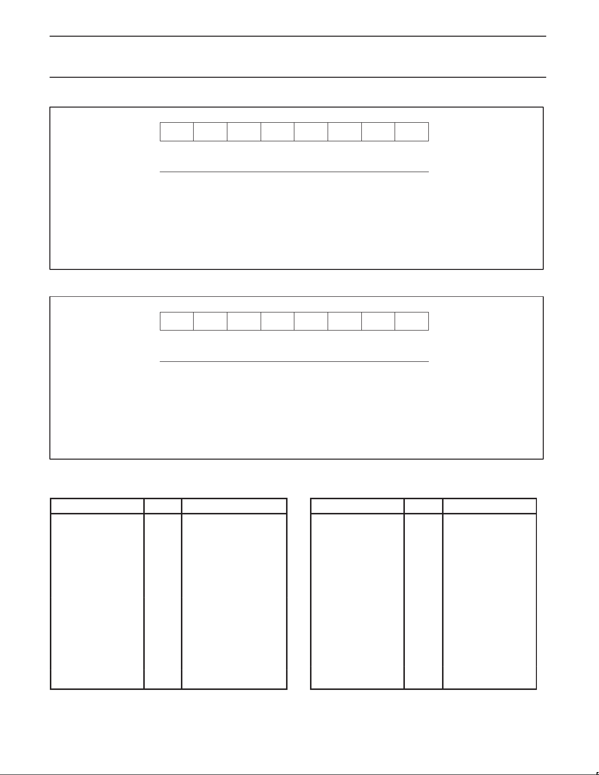
Philips Semiconductors Preliminary specification
80C51 8-bit microcontroller
16K/512 OTP/ROM/ROMless, 8 channel 10 bit A/D, I2C, PWM,
80C554/83C554/87C554
capture/compare, high I/O
01234567
IP1 (F8H)
IP1H (F7H)
PCT1PCT2PCT3PCM0PCM1PCM2PT2
BIT SYMBOL FUNCTION
IP1.7 PT2 T2 overflow interrupt(s) priority level
IP1.6 PCM2 T2 comparator 2 interrupt priority level
IP1.5 PCM1 T2 comparator 1 interrupt priority level
IP1.4 PCM0 T2 comparator 0 interrupt priority level
IP1.3 PCT3 T2 capture register 3 interrupt priority level
IP1.2 PCT2 T2 capture register 2 interrupt priority level
IP1.1 PCT1 T2 capture register 1 interrupt priority level
IP1.0 PCT0 T2 capture register 0 interrupt priority level
Figure 31. Interrupt Priority Register (IP1)
PCT1HPCT2HPCT3HPCM0HPCM1HPCM2HPT2H
PCT0
(LSB)(MSB)
SU00764
01234567
PCT0H
(LSB)(MSB)
BIT SYMBOL FUNCTION
IP1H.7 PT2H T2 overflow interrupt(s) priority level high
IP1H.6 PCM2H T2 comparator 2 interrupt priority level high
IP1H.5 PCM1H T2 comparator 1 interrupt priority level high
IP1H.4 PCM0H T2 comparator 0 interrupt priority level high
IP1H.3 PCT3H T2 capture register 3 interrupt priority level high
IP1H.2 PCT2H T2 capture register 2 interrupt priority level high
IP1H.1 PCT1H T2 capture register 1 interrupt priority level high
IP1H.0 PCT0H T2 capture register 0 interrupt priority level high
Figure 32. Interrupt Priority Register High (IP1H)
Table 3. Interrupt Priority Structure
SOURCE NAME PRIORITY WITHIN LEVEL
External interrupt 0 X0
SIO1 (I2C) S1
ADC completion ADC
Timer 0 overflow T0
T2 capture 0 CT0
T2 compare 0 CM0
External interrupt 1 X1
T2 capture 1 CT1
T2 compare 1 CM1
Timer 1 overflow T1
T2 capture 2 CT2
T2 compare 2 CM2
SIO0 (UART) S0
T2 capture 3 CT3
Timer T2 overflow T2 ↓
(highest)
↑
(lowest)
SU00984
Table 4. Interrupt Vector Addresses
SOURCE NAME VECTOR ADDRESS
External interrupt 0 X0 0003H
Timer 0 overflow T0 000BH
External interrupt 1 X1 0013H
Timer 1 overflow T1 001BH
SIO0 (UART) S0 0023H
SIO1 (I2C) S1 002BH
T2 capture 0 CT0 0033H
T2 capture 1 CT1 003BH
T2 capture 2 CT2 0043H
T2 capture 3 CT3 004BH
ADC completion ADC 0053H
T2 compare 0 CM0 005BH
T2 compare 1 CM1 0063H
T2 compare 2 CM2 006BH
T2 overflow T2 0073H
1999 Apr 07
31
Page 32

Philips Semiconductors Preliminary specification
80C51 8-bit microcontroller
16K/512 OTP/ROM/ROMless, 8 channel 10 bit A/D, I2C, PWM,
80C554/83C554/87C554
capture/compare, high I/O
2
C Serial I/O: The I2C bus uses two wires (SDA and SCL) to
SIO1, I
transfer information between devices connected to the bus. The
main features of the bus are:
– Bidirectional data transfer between masters and slaves
– Multimaster bus (no central master)
– Arbitration between simultaneously transmitting masters without
corruption of serial data on the bus
– Serial clock synchronization allows devices with dif ferent bit rates
to communicate via one serial bus
– Serial clock synchronization can be used as a handshake
mechanism to suspend and resume serial transfer
2
– The I
C bus may be used for test and diagnostic purposes
The output latches of P1.6 and P1.7 must be set to logic 1 in order
to enable SIO1.
The 8XC554 on-chip I
2
C bus specification and supports all transfer modes (other than
the I
the low-speed mode) from and to the I
2
C logic provides a serial interface that meets
2
C bus. The SIO1 logic
handles bytes transfer autonomously. It also keeps track of serial
transfers, and a status register (S1STA) reflects the status of SIO1
and the I
2
C bus.
The CPU interfaces to the I2C logic via the following four special
function registers: S1CON (SIO1 control register), S1STA (SIO1
status register), S1DAT (SIO1 data register), and S1ADR (SIO1
slave address register). The SIO1 logic interfaces to the external I
2
bus via two port 1 pins: P1.6/SCL (serial clock line) and P1.7/SDA
(serial data line).
A typical I
2
C bus configuration is shown in Figure 33, and Figure 34
shows how a data transfer is accomplished on the bus. Depending
on the state of the direction bit (R/W), two types of data transfers are
possible on the I
2
C bus:
1. Data transfer from a master transmitter to a slave receiver. The
first byte transmitted by the master is the slave address. Next
follows a number of data bytes. The slave returns an
acknowledge bit after each received byte.
2. Data transfer from a slave transmitter to a master receiver. The
first byte (the slave address) is transmitted by the master. The
slave then returns an acknowledge bit. Next follows the data
bytes transmitted by the slave to the master. The master returns
an acknowledge bit after all received bytes other than the last
byte. At the end of the last received byte, a “not acknowledge” is
returned.
The master device generates all of the serial clock pulses and the
START and STOP conditions. A transfer is ended with a STOP
condition or with a repeated STAR T condition. Since a repeated
STAR T condition is also the beginning of the next serial transfer, the
2
I
C bus will not be released.
Modes of Operation: The on-chip SIO1 logic may operate in the
following four modes:
1. Master Transmitter Mode:
Serial data output through P1.7/SDA while P1.6/SCL outputs the
serial clock. The first byte transmitted contains the slave address
of the receiving device (7 bits) and the data direction bit. In this
case the data direction bit (R/W
) will be logic 0, and we say that
a “W” is transmitted. Thus the first byte transmitted is SLA+W.
Serial data is transmitted 8 bits at a time. After each byte is
transmitted, an acknowledge bit is received. STAR T and STOP
conditions are output to indicate the beginning and the end of a
serial transfer.
2. Master Receiver Mode:
The first byte transmitted contains the slave address of the
transmitting device (7 bits) and the data direction bit. In this case
the data direction bit (R/W
) will be logic 1, and we say that an “R”
is transmitted. Thus the first byte transmitted is SLA+R. Serial
data is received via P1.7/SDA while P1.6/SCL outputs the serial
clock. Serial data is received 8 bits at a time. After each byte is
received, an acknowledge bit is transmitted. STAR T and STOP
conditions are output to indicate the beginning and end of a
serial transfer.
3. Slave Receiver Mode:
C
Serial data and the serial clock are received through P1.7/SDA
and P1.6/SCL. After each byte is received, an acknowledge bit is
transmitted. ST ART and STOP conditions are recognized as the
beginning and end of a serial transfer. Address recognition is
performed by hardware after reception of the slave address and
direction bit.
4. Slave Transmitter Mode:
The first byte is received and handled as in the slave receiver
mode. However, in this mode, the direction bit will indicate that
the transfer direction is reversed. Serial data is transmitted via
P1.7/SDA while the serial clock is input through P1.6/SCL.
STAR T and ST OP conditions are recognized as the beginning
and end of a serial transfer.
In a given application, SIO1 may operate as a master and as a
slave. In the slave mode, the SIO1 hardware looks for its own slave
address and the general call address. If one of these addresses is
detected, an interrupt is requested. When the microcontroller wishes
to become the bus master, the hardware waits until the bus is free
before the master mode is entered so that a possible slave action is
not interrupted. If bus arbitration is lost in the master mode, SIO1
switches to the slave mode immediately and can detect its own
slave address in the same serial transfer.
1999 Apr 07
32
Page 33
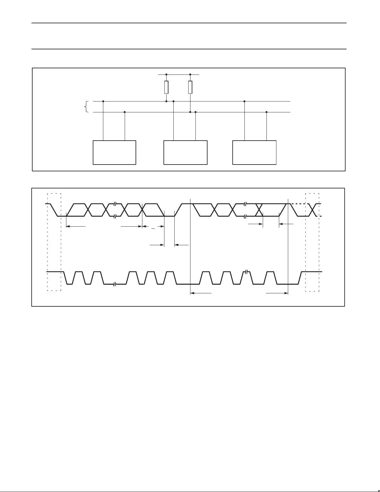
Philips Semiconductors Preliminary specification
80C51 8-bit microcontroller
16K/512 OTP/ROM/ROMless, 8 channel 10 bit A/D, I2C, PWM,
80C554/83C554/87C554
capture/compare, high I/O
V
DD
SDA
2
I
C bus
MSB
P1.7/SDA P1.6/SCL
8XC554
SLAVE ADDRESS
R
P
OTHER DEVICE WITH
2
I
C INTERFACE
R
P
Figure 33. Typical I2C Bus Configuration
R/W
DIRECTION
BIT
ACKNOWLEDGMENT
SIGNAL FROM RECEIVER
CLOCK LINE HELD LOW WHILE
INTERRUPTS ARE SERVICED
OTHER DEVICE WITH
I2C INTERFACE
ACKNOWLEDGMENT
SIGNAL FROM RECEIVER
SDA
SCL
SU00964
STOP
CONDITION
REPEATED
START
CONDITION
SCL
CONDITION
S
START
1 2 7 8 9 1 2 3–8
ACK
Figure 34. Data Transfer on the I2C Bus
SIO1 Implementation and Operation: Figure 35 shows how the
on-chip I
2
C bus interface is implemented, and the following text
describes the individual blocks.
I
NPUT FILTERS AND OUTPUT STAGES
The input filters have I2C compatible input levels. If the input voltage
is less than 1.5V , the input logic level is interpreted as 0; if the input
voltage is greater than 3.0V , the input logic level is interpreted as 1.
Input signals are synchronized with the internal clock (f
OSC
/4), and
spikes shorter than three oscillator periods are filtered out.
The output stages consist of open drain transistors that can sink
3mA at V
clamping diodes to V
bus and V
A
DDRESS REGISTER, S1ADR
< 0.4V . These open drain outputs do not have
OUT
is switched off, the I2C bus is not affected.
DD
. Thus, if the device is connected to the I2C
DD
This 8-bit special function register may be loaded with the 7-bit slave
address (7 most significant bits) to which SIO1 will respond when
programmed as a slave transmitter or receiver. The LSB (GC) is
used to enable general call address (00H) recognition.
9
REPEATED IF MORE BYTES
ARE TRANSFERRED
C
OMPARATOR
ACK
P/S
SU00965
The comparator compares the received 7-bit slave address with its
own slave address (7 most significant bits in S1ADR). It also
compares the first received 8-bit byte with the general call address
(00H). If an equality is found, the appropriate status bits are set and
an interrupt is requested.
S
HIFT REGISTER, S1DAT
This 8-bit special function register contains a byte of serial data to
be transmitted or a byte which has just been received. Data in
S1DAT is always shifted from right to left; the first bit to be
transmitted is the MSB (bit 7) and, after a byte has been received,
the first bit of received data is located at the MSB of S1DAT. While
data is being shifted out, data on the bus is simultaneously being
shifted in; S1DAT always contains the last byte present on the bus.
Thus, in the event of lost arbitration, the transition from master
transmitter to slave receiver is made with the correct data in S1DAT.
1999 Apr 07
33
Page 34
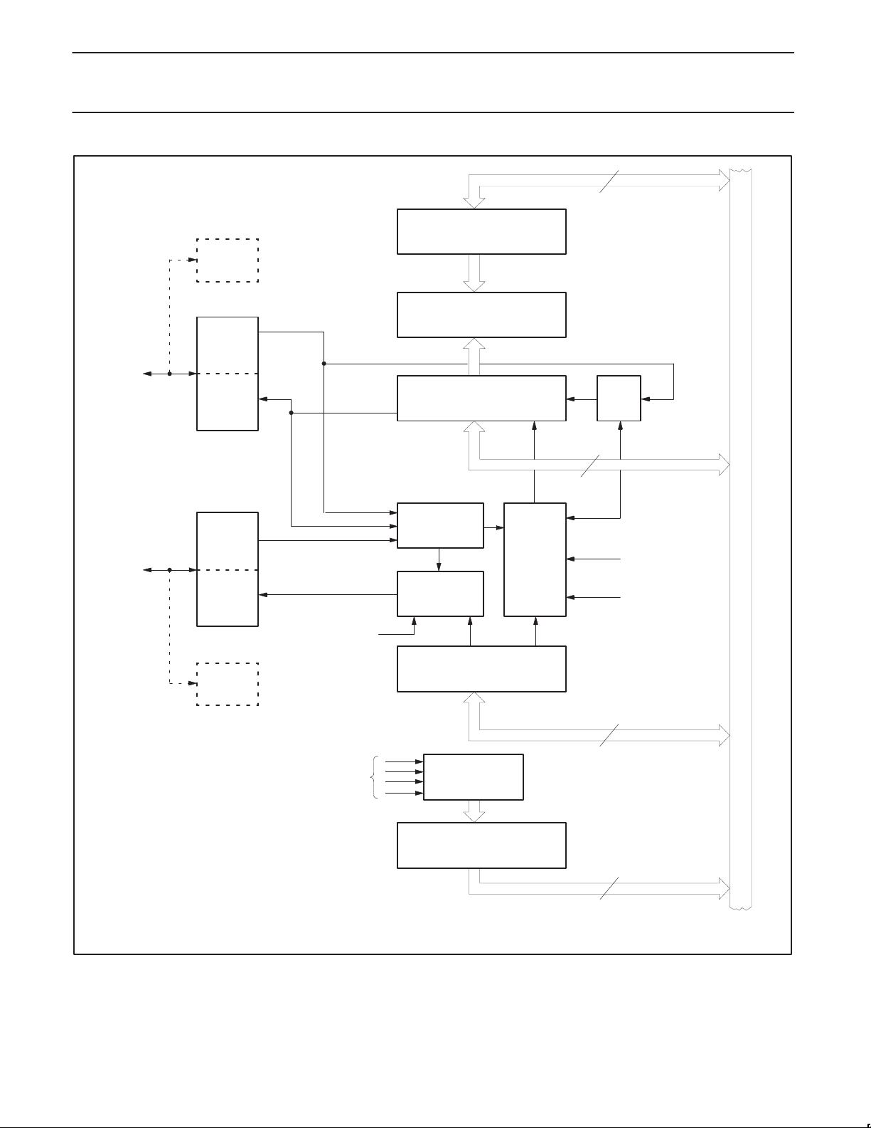
Philips Semiconductors Preliminary specification
80C51 8-bit microcontroller
16K/512 OTP/ROM/ROMless, 8 channel 10 bit A/D, I2C, PWM,
80C554/83C554/87C554
capture/compare, high I/O
8
P1.7/SDA
P1.6/SCL
P1.7
INPUT
FILTER
OUTPUT
STAGE
INPUT
FILTER
OUTPUT
STAGE
TIMER 1
OVERFLOW
S1ADR
S1DAT
ADDRESS REGISTER
COMPARATOR
SHIFT REGISTER
ARBITRATION &
SYNC LOGIC
SERIAL CLOCK
GENERATOR
TIMING
&
CONTROL
LOGIC
ACK
8
f
/4
OSC
INTERRUPT
INTERNAL BUS
P1.6
S1CON
STATUS BITS
S1STA
CONTROL REGISTER
STATUS
DECODER
STATUS REGISTER
Figure 35. I2C Bus Serial Interface Block Diagram
8
8
su00966
1999 Apr 07
34
Page 35
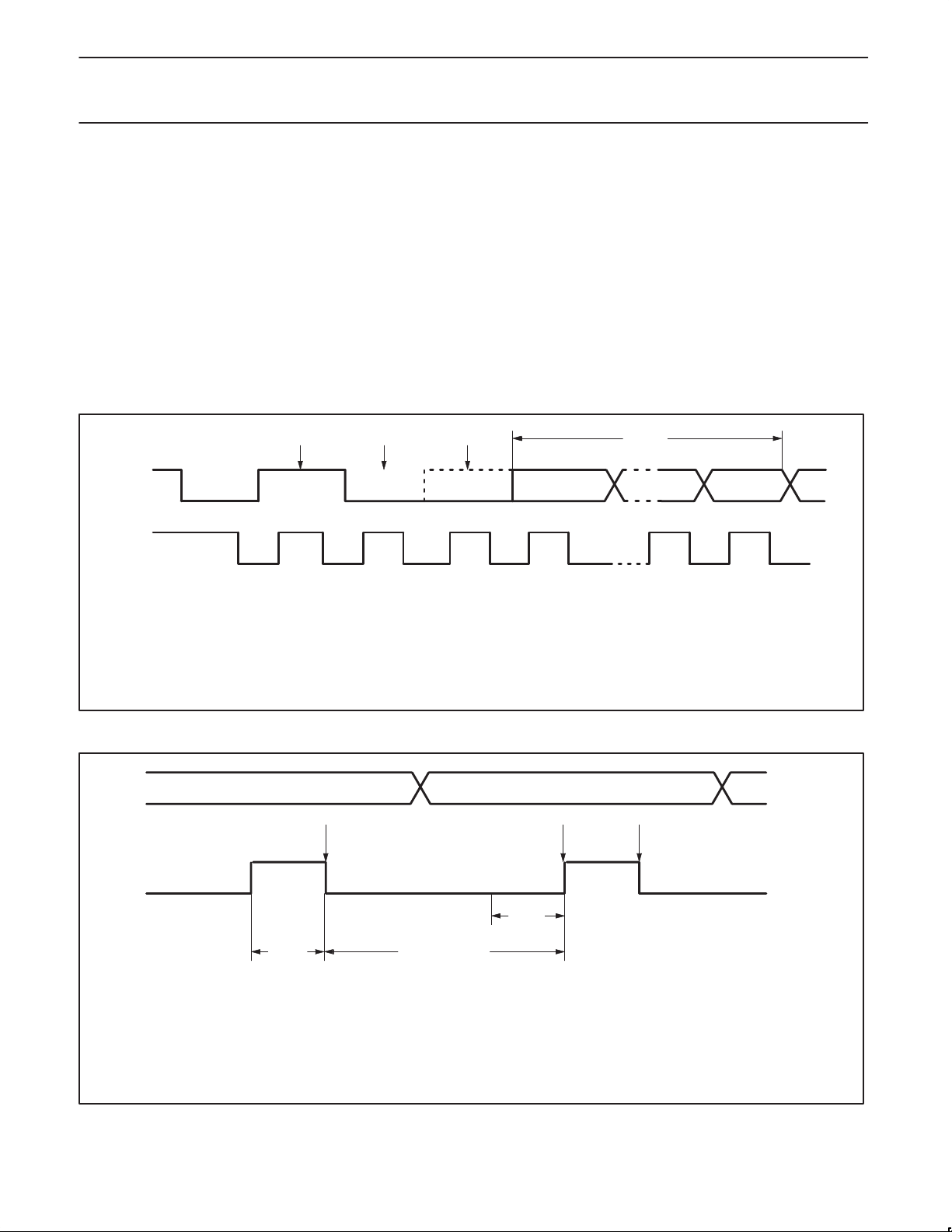
Philips Semiconductors Preliminary specification
80C51 8-bit microcontroller
16K/512 OTP/ROM/ROMless, 8 channel 10 bit A/D, I2C, PWM,
80C554/83C554/87C554
capture/compare, high I/O
RBITRATION AND SYNCHRONIZATION LOGIC
A
In the master transmitter mode, the arbitration logic checks that
every transmitted logic 1 actually appears as a logic 1 on the I
2
C
bus. If another device on the bus overrules a logic 1 and pulls the
SDA line low, arbitration is lost, and SIO1 immediately changes from
master transmitter to slave receiver. SIO1 will continue to output
clock pulses (on SCL) until transmission of the current serial byte is
complete.
Arbitration may also be lost in the master receiver mode. Loss of
arbitration in this mode can only occur while SIO1 is returning a “not
acknowledge: (logic 1) to the bus. Arbitration is lost when another
device on the bus pulls this signal LOW. Since this can occur only at
the end of a serial byte, SIO1 generates no further clock pulses.
The synchronization logic will synchronize the serial clock generator
with the clock pulses on the SCL line from another device. If two or
more master devices generate clock pulses, the “mark” duration is
determined by the device that generates the shortest “marks,” and
the “space” duration is determined by the device that generates the
longest “spaces.” Figure 37 shows the synchronization procedure.
A slave may stretch the space duration to slow down the bus
master. The space duration may also be stretched for handshaking
purposes. This can be done after each bit or after a complete byte
transfer. SIO1 will stretch the SCL space duration after a byte has
been transmitted or received and the acknowledge bit has been
transferred. The serial interrupt flag (SI) is set, and the stretching
continues until the serial interrupt flag is cleared.
Figure 36 shows the arbitration procedure.
(3)
SDA
SCL
(1) (1) (2)
1
234 89
1. Another device transmits identical serial data.
2. Another device overrules a logic 1 (dotted line) transmitted by SIO1 (master) by pulling the SDA line low. Arbitration is
lost, and SIO1 enters the slave receiver mode.
3. SIO1 is in the slave receiver mode but still generates clock pulses until the current byte has been transmitted. SIO1 will
not generate clock pulses for the next byte. Data on SDA originates from the new master once it has won arbitration.
ACK
SU00967
Figure 36. Arbitration Procedure
SDA
SCL
MARK
DURATION
(1)
(2)
SPACE DURATION
(3) (1)
1. Another service pulls the SCL line low before the SIO1 “mark” duration is complete. The serial clock generator is immediately
reset and commences with the “space” duration by pulling SCL low.
2. Another device still pulls the SCL line low after SIO1 releases SCL. The serial clock generator is forced into the wait state
until the SCL line is released.
3. The SCL line is released, and the serial clock generator commences with the mark duration.
SU00968
Figure 37. Serial Clock Synchronization
1999 Apr 07
35
Page 36

Philips Semiconductors Preliminary specification
80C51 8-bit microcontroller
16K/512 OTP/ROM/ROMless, 8 channel 10 bit A/D, I2C, PWM,
80C554/83C554/87C554
capture/compare, high I/O
ERIAL CLOCK GENERATOR
S
This programmable clock pulse generator provides the SCL clock
pulses when SIO1 is in the master transmitter or master receiver
mode. It is switched off when SIO1 is in a slave mode. The
programmable output clock frequencies are: f
OSC
/120, f
OSC
/9600,
and the Timer 1 overflow rate divided by eight. The output clock
pulses have a 50% duty cycle unless the clock generator is
synchronized with other SCL clock sources as described above.
T
IMING AND CONTROL
The timing and control logic generates the timing and control signals
for serial byte handling. This logic block provides the shift pulses for
S1DAT, enables the comparator, generates and detects start and
stop conditions, receives and transmits acknowledge bits, controls
the master and slave modes, contains interrupt request logic, and
monitors the I
2
C bus status.
CONTROL REGISTER, S1CON
This 7-bit special function register is used by the microcontroller to
control the following SIO1 functions: start and restart of a serial
transfer, termination of a serial transfer, bit rate, address recognition,
and acknowledgment.
S
TATUS DECODER AND STATUS REGISTER
The status decoder takes all of the internal status bits and
compresses them into a 5-bit code. This code is unique for each I
2
C
bus status. The 5-bit code may be used to generate vector
addresses for fast processing of the various service routines. Each
service routine processes a particular bus status. There are 26
possible bus states if all four modes of SIO1 are used. The 5-bit
status code is latched into the five most significant bits of the status
register when the serial interrupt flag is set (by hardware) and
remains stable until the interrupt flag is cleared by software. The
three least significant bits of the status register are always zero. If
the status code is used as a vector to service routines, then the
routines are displaced by eight address locations. Eight bytes of
code is sufficient for most of the service routines (see the software
example in this section).
The Four SIO1 Special Function Registers: The microcontroller
interfaces to SIO1 via four special function registers. These four
SFRs (S1ADR, S1DAT, S1CON, and S1STA) are described
individually in the following sections.
The Address Register, S1ADR: The CPU can read from and write
to this 8-bit, directly addressable SFR. S1ADR is not affected by the
SIO1 hardware. The contents of this register are irrelevant when
SIO1 is in a master mode. In the slave modes, the seven most
significant bits must be loaded with the microcontroller’s own slave
address, and, if the least significant bit is set, the general call
address (00H) is recognized; otherwise it is ignored.
65 43210
7
S1ADR (DBH) XGC
The most significant bit corresponds to the first bit received from the
2
I
C bus after a start condition. A logic 1 in S1ADR corresponds to a
high level on the I
X XXXX X
own slave address
2
C bus, and a logic 0 corresponds to a low level
on the bus.
The Data Register, S1DAT: S1DAT contains a byte of serial data to
be transmitted or a byte which has just been received. The CPU can
read from and write to this 8-bit, directly addressable SFR while it is
not in the process of shifting a byte. This occurs when SIO1 is in a
defined state and the serial interrupt flag is set. Data in S1DAT
remains stable as long as SI is set. Data in S1DAT is always shifted
from right to left: the first bit to be transmitted is the MSB (bit 7), and,
after a byte has been received, the first bit of received data is
located at the MSB of S1DAT. While data is being shifted out, data
on the bus is simultaneously being shifted in; S1DAT always
contains the last data byte present on the bus. Thus, in the event of
lost arbitration, the transition from master transmitter to slave
receiver is made with the correct data in S1DAT.
65 43210
7
S1DAT (DAH) SD7 SD6 SD5 SD4 SD3 SD2 SD1 SD0
shift direction
SD7 - SD0:
Eight bits to be transmitted or just received. A logic 1 in S1DAT
corresponds to a high level on the I
corresponds to a low level on the bus. Serial data shifts through
S1DAT from right to left. Figure 38 shows how data in S1DAT is
serially transferred to and from the SDA line.
S1DAT and the ACK flag form a 9-bit shift register which shifts in or
shifts out an 8-bit byte, followed by an acknowledge bit. The ACK
flag is controlled by the SIO1 hardware and cannot be accessed by
the CPU. Serial data is shifted through the ACK flag into S1DAT on
the rising edges of serial clock pulses on the SCL line. When a byte
has been shifted into S1DAT, the serial data is available in S1DAT,
and the acknowledge bit is returned by the control logic during the
ninth clock pulse. Serial data is shifted out from S1DAT via a buf fer
(BSD7) on the falling edges of clock pulses on the SCL line.
When the CPU writes to S1DAT, BSD7 is loaded with the content of
S1DAT.7, which is the first bit to be transmitted to the SDA line (see
Figure 39). After nine serial clock pulses, the eight bits in S1DAT will
have been transmitted to the SDA line, and the acknowledge bit will
be present in ACK. Note that the eight transmitted bits are shifted
back into S1DAT.
The Control Register, S1CON: The CPU can read from and write
to this 8-bit, directly addressable SFR. Two bits are affected by the
SIO1 hardware: the SI bit is set when a serial interrupt is requested,
and the STO bit is cleared when a STOP condition is present on the
2
I
C bus. The STO bit is also cleared when ENS1 = “0”.
7
6543210
S1CON (D8H) ENS1 STA STO SI AA CR1 CR0
CR2
ENS1, THE SIO1 ENABLE BIT
ENS1 = “0”: When ENS1 is “0”, the SDA and SCL outputs are in a
high impedance state. SDA and SCL input signals are ignored, SIO1
is in the “not addressed” slave state, and the STO bit in S1CON is
forced to “0”. No other bits are affected. P1.6 and P1.7 may be used
as open drain I/O ports.
ENS1 = “1”: When ENS1 is “1”, SIO1 is enabled. The P1.6 and P1.7
port latches must be set to logic 1.
ENS1 should not be used to temporarily release SIO1 from the I2C
bus since, when ENS1 is reset, the I2C bus status is lost. The AA
flag should be used instead (see description of the AA flag in the
following text).
2
C bus, and a logic 0
1999 Apr 07
36
Page 37
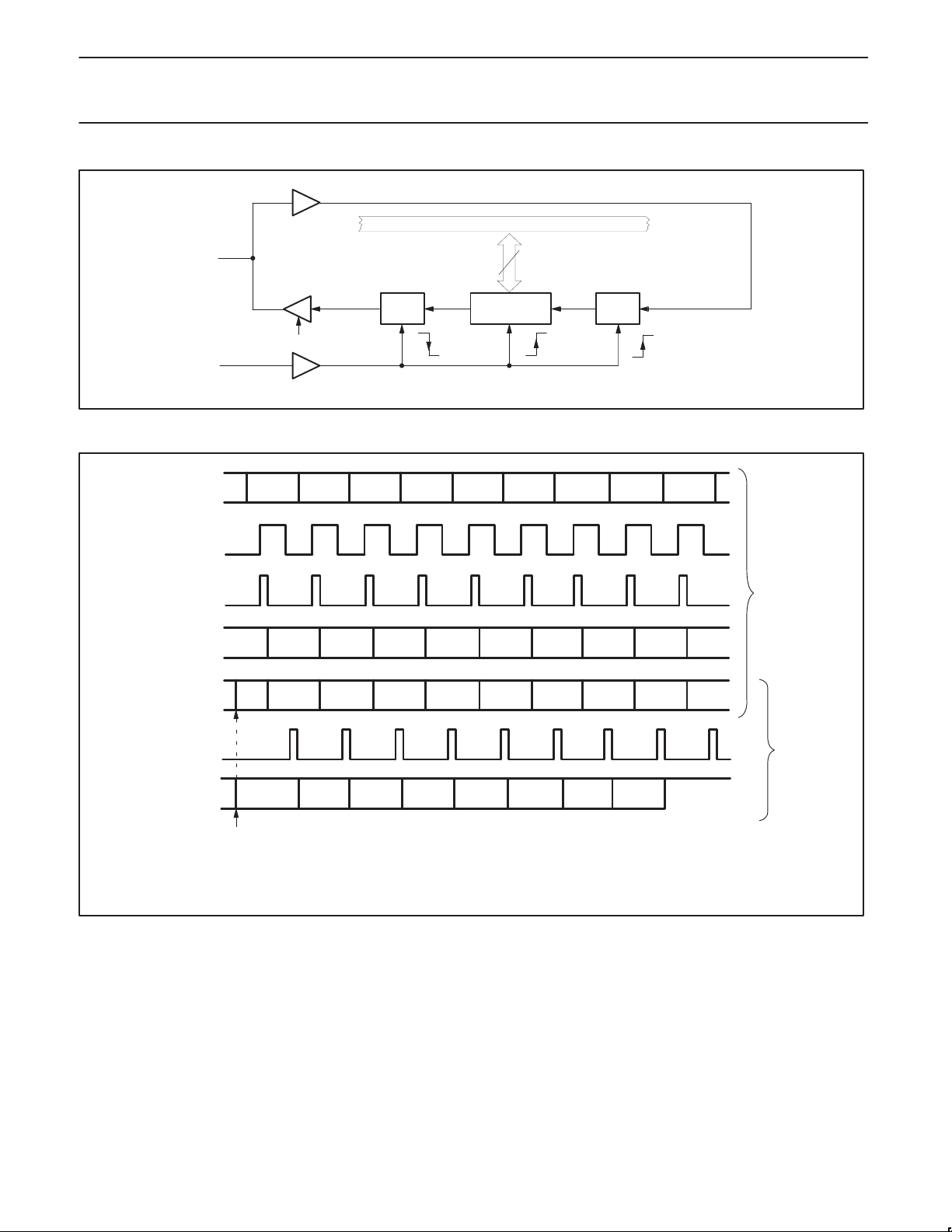
Philips Semiconductors Preliminary specification
80C51 8-bit microcontroller
16K/512 OTP/ROM/ROMless, 8 channel 10 bit A/D, I2C, PWM,
80C554/83C554/87C554
capture/compare, high I/O
INTERNAL BUS
SDA
SCL
SDA
SCL
SHIFT ACK & S1DAT
ACK
8
BSD7 S1DAT ACK
SHIFT PULSES
SU00969
Figure 38. Serial Input/Output Configuration
D7 D6 D5 D4 D3 D2 D1 D0 A
SHIFT IN
(2) (2) (2) (2) (2) (2) (2) (2) A
(2) (2) (2) (2) (2) (2) (2) (2) (1)(1)S1DAT
SHIFT BSD7
BSD7
(1) Valid data in S1DAT
(2) Shifting data in S1DAT and ACK
(3) High level on SDA
D7 D6 D5 D4 D3 D2 D1 D0 (3)
LOADED BY THE CPU
Figure 39. Shift-in and Shift-out Timing
In the following text, it is assumed that ENS1 = “1”.
STA, THE START FLAG
STA = “1”: When the STA bit is set to enter a master mode, the SIO1
hardware checks the status of the I2C bus and generates a START
condition if the bus is free. If the bus is not free, then SIO1 waits for
a STOP condition (which will free the bus) and generates a START
condition after a delay of a half clock period of the internal serial
clock generator.
If STA is set while SIO1 is already in a master mode and one or
more bytes are transmitted or received, SIO1 transmits a repeated
START condition. STA may be set at any time. STA may also be set
when SIO1 is an addressed slave.
SHIFT OUT
SU00970
STA = “0”: When the STA bit is reset, no START condition or
repeated START condition will be generated.
STO
, THE STOP FLAG
STO = “1”: When the STO bit is set while SIO1 is in a master mode,
a STOP condition is transmitted to the I
2
C bus. When the STOP
condition is detected on the bus, the SIO1 hardware clears the STO
flag. In a slave mode, the STO flag may be set to recover from an
error condition. In this case, no STOP condition is transmitted to the
2
I
C bus. However, the SIO1 hardware behaves as if a STOP
condition has been received and switches to the defined “not
addressed” slave receiver mode. The STO flag is automatically
cleared by hardware.
1999 Apr 07
37
Page 38

Philips Semiconductors Preliminary specification
80C51 8-bit microcontroller
16K/512 OTP/ROM/ROMless, 8 channel 10 bit A/D, I2C, PWM,
80C554/83C554/87C554
capture/compare, high I/O
If the STA and STO bits are both set, the a STOP condition is
transmitted to the I
2
C bus if SIO1 is in a master mode (in a slave
mode, SIO1 generates an internal STOP condition which is not
transmitted). SIO1 then transmits a STAR T condition.
STO = “0”: When the STO bit is reset, no STOP condition will be
generated.
SI
, THE SERIAL INTERRUPT FLAG
SI = “1”: When the SI flag is set, then, if the EA and ES1 (interrupt
enable register) bits are also set, a serial interrupt is requested. SI is
set by hardware when one of 25 of the 26 possible SIO1 states is
entered. The only state that does not cause SI to be set is state
F8H, which indicates that no relevant state information is available.
While SI is set, the low period of the serial clock on the SCL line is
stretched, and the serial transfer is suspended. A high level on the
SCL line is unaffected by the serial interrupt flag. SI must be reset
by software.
SI = “0”: When the SI flag is reset, no serial interrupt is requested,
and there is no stretching of the serial clock on the SCL line.
AA
, THE ASSERT ACKNOWLEDGE FLAG
AA = “1”: If the AA flag is set, an acknowledge (low level to SDA) will
be returned during the acknowledge clock pulse on the SCL line
when:
– The “own slave address” has been received
– The general call address has been received while the general call
bit (GC) in S1ADR is set
– A data byte has been received while SIO1 is in the master
receiver mode
– A data byte has been received while SIO1 is in the addressed
slave receiver mode
AA = “0”: if the AA flag is reset, a not acknowledge (high level to
SDA) will be returned during the acknowledge clock pulse on SCL
when:
– A data has been received while SIO1 is in the master receiver
mode
– A data byte has been received while SIO1 is in the addressed
slave receiver mode
When SIO1 is in the addressed slave transmitter mode, state C8H
will be entered after the last serial is transmitted (see Figure 43).
When SI is cleared, SIO1 leaves state C8H, enters the not
addressed slave receiver mode, and the SDA line remains at a high
level. In state C8H, the AA flag can be set again for future address
recognition.
When SIO1 is in the not addressed slave mode, its own slave
address and the general call address are ignored. Consequently, no
acknowledge is returned, and a serial interrupt is not requested.
Thus, SIO1 can be temporarily released from the I
2
C bus while the
bus status is monitored. While SIO1 is released from the bus,
STAR T and STOP conditions are detected, and serial data is shifted
in. Address recognition can be resumed at any time by setting the
AA flag. If the AA flag is set when the part’s own slave address or
the general call address has been partly received, the address will
be recognized at the end of the byte transmission.
CR
0, CR1, AND CR2, THE CLOCK RATE BITS
These three bits determine the serial clock frequency when SIO1 is
in a master mode. The various serial rates are shown in Table 5.
2
A 12.5kHz bit rate may be used by devices that interface to the I
C
bus via standard I/O port lines which are software driven and slow.
100kHz is usually the maximum bit rate and can be derived from a
16MHz, 12MHz, or a 6MHz oscillator. A variable bit rate (0.5kHz to
62.5kHz) may also be used if Timer 1 is not required for any other
purpose while SIO1 is in a master mode.
The frequencies shown in Table 5 are unimportant when SIO1 is in a
slave mode. In the slave modes, SIO1 will automatically synchronize
with any clock frequency up to 100kHz.
The Status Register, S1STA: S1STA is an 8-bit read-only special
function register. The three least significant bits are always zero.
The five most significant bits contain the status code. There are 26
possible status codes. When S1STA contains F8H, no relevant state
information is available and no serial interrupt is requested. All other
S1STA values correspond to defined SIO1 states. When each of
these states is entered, a serial interrupt is requested (SI = “1”). A
valid status code is present in S1STA one machine cycle after SI is
set by hardware and is still present one machine cycle after SI has
been reset by software.
Table 5. Serial Clock Rates
BIT FREQUENCY (kHz) AT f
CR2 CR1 CR0 6MHz 12MHz 16MHz 24MHz
0 0 0 23 47 62.5 94 117
0 0 1 27 54 71 107
0 1 0 31 63 83.3 125
0 1 1 37 75 100 150
1 0 0 6.25 12.5 17 25 31 960
1 0 1 50 100 133
1 1 0 100 200 267
1 1 1 0.24 < 62.5
0 < 255
0.49 < 62.5
0 < 254
NOTES:
1. These frequencies exceed the upper limit of 100kHz of the I
2. At f
= 24MHz/30MHz the maximum I2C bus rate of 100kHz cannot be realized due to the fixed divider rates.
OSC
1
1
0.65 < 55.6
0 < 253
2
C-bus specification and cannot be used in an I2C-bus application.
1999 Apr 07
38
OSC
2
1
1
1
1
200
1
400
0.98 < 50.0
0 < 251
2
30MHz
1
1
134
1
156
1
188
1
250
1
500
1.22 < 52.1
0 < 250
f
OSC
96 × (256 – (reload value Timer 1))
Reload value Timer 1 in Mode 2.
DIVIDED BY
256
224
192
160
120
60
Page 39

Philips Semiconductors Preliminary specification
80C51 8-bit microcontroller
16K/512 OTP/ROM/ROMless, 8 channel 10 bit A/D, I2C, PWM,
80C554/83C554/87C554
capture/compare, high I/O
More Information on SIO1 Operating Modes: The four operating
modes are:
– Master Transmitter
– Master Receiver
– Slave Receiver
– Slave Transmitter
Data transfers in each mode of operation are shown in Figures
40–43. These figures contain the following abbreviations:
Abbreviation Explanation
S Start condition
SLA 7-bit slave address
R Read bit (high level at SDA)
W Write bit (low level at SDA)
A Acknowledge bit (low level at SDA)
A
Not acknowledge bit (high level at SDA)
Data 8-bit data byte
P Stop condition
In Figures 40-43, circles are used to indicate when the serial
interrupt flag is set. The numbers in the circles show the status code
held in the S1STA register. At these points, a service routine must
be executed to continue or complete the serial transfer. These
service routines are not critical since the serial transfer is suspended
until the serial interrupt flag is cleared by software.
When a serial interrupt routine is entered, the status code in S1STA
is used to branch to the appropriate service routine. For each status
code, the required software action and details of the following serial
transfer are given in Tables 6-10.
Master Transmitter Mode: In the master transmitter mode, a
number of data bytes are transmitted to a slave receiver (see
Figure 40). Before the master transmitter mode can be entered,
S1CON must be initialized as follows:
7
6543210
S1CON (D8H) CR2 ENS1 STA STO SI AA CR1 CR0
bit
rate
1000X
bit rate
CR0, CR1, and CR2 define the serial bit rate. ENS1 must be set to
logic 1 to enable SIO1. If the AA bit is reset, SIO1 will not
acknowledge its own slave address or the general call address in
the event of another device becoming master of the bus. In other
words, if AA is reset, SIO0 cannot enter a slave mode. STA, STO,
and SI must be reset.
The master transmitter mode may now be entered by setting the
STA bit using the SETB instruction. The SIO1 logic will now test the
2
I
C bus and generate a start condition as soon as the bus becomes
free. When a STAR T condition is transmitted, the serial interrupt flag
(SI) is set, and the status code in the status register (S1STA) will be
08H. This status code must be used to vector to an interrupt service
routine that loads S1DA T with the slave address and the data
direction bit (SLA+W). The SI bit in S1CON must then be reset
before the serial transfer can continue.
When the slave address and the direction bit have been transmitted
and an acknowledgment bit has been received, the serial interrupt
flag (SI) is set again, and a number of status codes in S1STA are
possible. There are 18H, 20H, or 38H for the master mode and also
68H, 78H, or B0H if the slave mode was enabled (AA = logic 1). The
appropriate action to be taken for each of these status codes is
detailed in Table 6. After a repeated start condition (state 10H). SIO1
may switch to the master receiver mode by loading S1DAT with
SLA+R).
Master Receiver Mode: In the master receiver mode, a number of
data bytes are received from a slave transmitter (see Figure 41).
The transfer is initialized as in the master transmitter mode. When
the start condition has been transmitted, the interrupt service routine
must load S1DAT with the 7-bit slave address and the data direction
bit (SLA+R). The SI bit in S1CON must then be cleared before the
serial transfer can continue.
When the slave address and the data direction bit have been
transmitted and an acknowledgment bit has been received, the
serial interrupt flag (SI) is set again, and a number of status codes in
S1STA are possible. These are 40H, 48H, or 38H for the master
mode and also 68H, 78H, or B0H if the slave mode was enabled
(AA = logic 1). The appropriate action to be taken for each of these
status codes is detailed in Table 7. ENS1, CR1, and CR0 are not
affected by the serial transfer and are not referred to in Table 7. After
a repeated start condition (state 10H), SIO1 may switch to the
master transmitter mode by loading S1DAT with SLA+W.
Slave Receiver Mode: In the slave receiver mode, a number of
data bytes are received from a master transmitter (see Figure 42).
To initiate the slave receiver mode, S1ADR and S1CON must be
loaded as follows:
7
65 4321 0
S1ADR (DBH) XGC
X XXXXX
own slave address
The upper 7 bits are the address to which SIO1 will respond when
addressed by a master. If the LSB (GC) is set, SIO1 will respond to
the general call address (00H); otherwise it ignores the general call
address.
6543210
7
S1CON (D8H) ENS1 STA STO SI AA CR1 CR0
CR2
X1 0001X X
CR0, CR1, and CR2 do not affect SIO1 in the slave mode. ENS1
must be set to logic 1 to enable SIO1. The AA bit must be set to
enable SIO1 to acknowledge its own slave address or the general
call address. STA, STO, and SI must be reset.
When S1ADR and S1CON have been initialized, SIO1 waits until it
is addressed by its own slave address followed by the data direction
bit which must be “0” (W) for SIO1 to operate in the slave receiver
mode. After its own slave address and the W bit have been
received, the serial interrupt flag (I) is set and a valid status code
can be read from S1STA. This status code is used to vector to an
interrupt service routine, and the appropriate action to be taken for
each of these status codes is detailed in Table 8. The slave receiver
mode may also be entered if arbitration is lost while SIO1 is in the
master mode (see status 68H and 78H).
If the AA bit is reset during a transfer, SIO1 will return a not
acknowledge (logic 1) to SDA after the next received data byte.
While AA is reset, SIO1 does not respond to its own slave address
or a general call address. However, the I
2
C bus is still monitored
and address recognition may be resumed at any time by setting AA.
This means that the AA bit may be used to temporarily isolate SIO1
from the I
2
C bus.
1999 Apr 07
39
Page 40
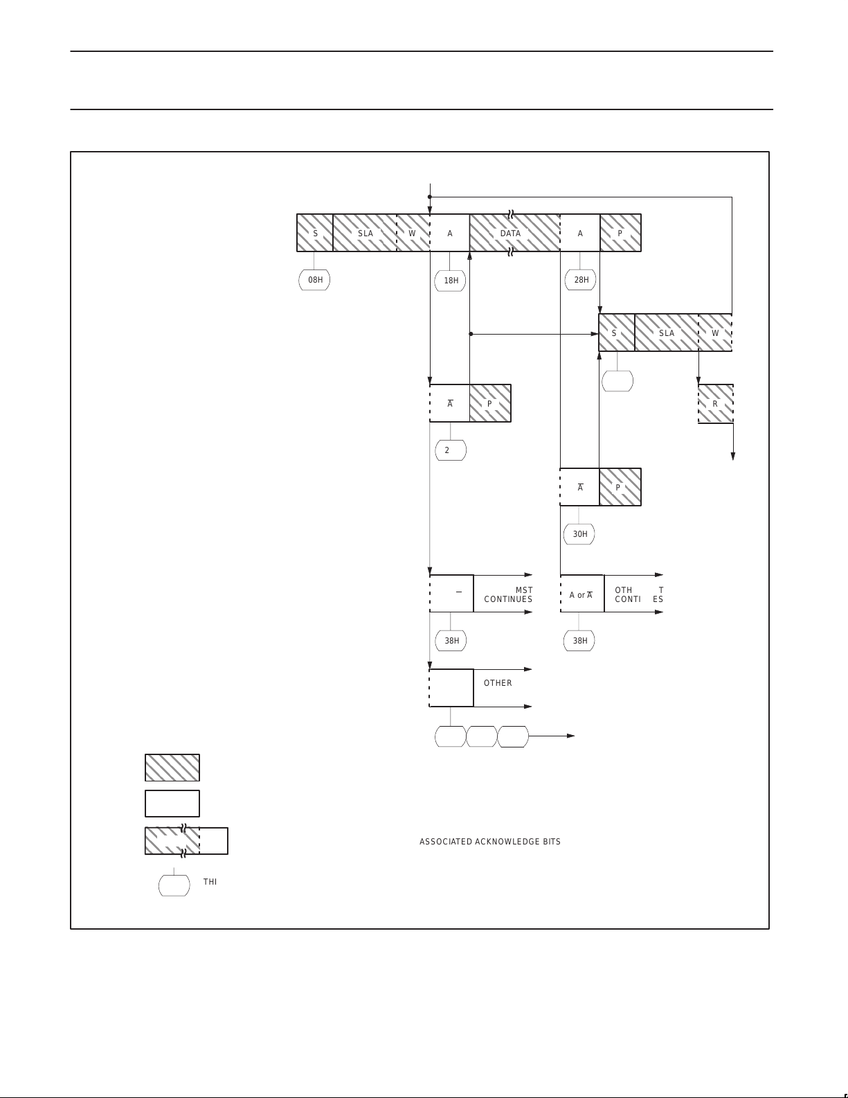
Philips Semiconductors Preliminary specification
80C51 8-bit microcontroller
16K/512 OTP/ROM/ROMless, 8 channel 10 bit A/D, I2C, PWM,
80C554/83C554/87C554
capture/compare, high I/O
MT
SUCCESSFUL TRANSMISSION
TO A SLAVE RECEIVER
NEXT TRANSFER STARTED WITH A REPEATED START CONDITION
NOT ACKNOWLEDGE RECEIVED AFTER THE SLAVE ADDRESS
NOT ACKNOWLEDGE RECEIVED AFTER A DATA BYTE
ARBITRATION LOST IN SLAVE ADDRESS OR DATA BYTE
S SLA WA ADATA P
08H
18H
A P
20H
A or A
OTHER MST
CONTINUES
28H
A P
30H
A or A
S SLA W
10H
TO MST/REC MODE
ENTRY = MR
OTHER MST
CONTINUES
R
ARBITRATION LOST AND ADDRESSED AS SLAVE
FROM MASTER TO SLAVE
FROM SLAVE TO MASTER
Data
A
ANY NUMBER OF DATA BYTES AND THEIR ASSOCIATED ACKNOWLEDGE BITS
THIS NUMBER (CONTAINED IN S1STA) CORRESPONDS TO A DEFINED STATE OF THE I
n
Figure 40. Format and States in the Master Transmitter Mode
38H
OTHER MST
A
CONTINUES
68H 78H 80H
38H
TO CORRESPONDING
STATES IN SLAVE MODE
2
C BUS. SEE TABLE 6.
SU00971
1999 Apr 07
40
Page 41
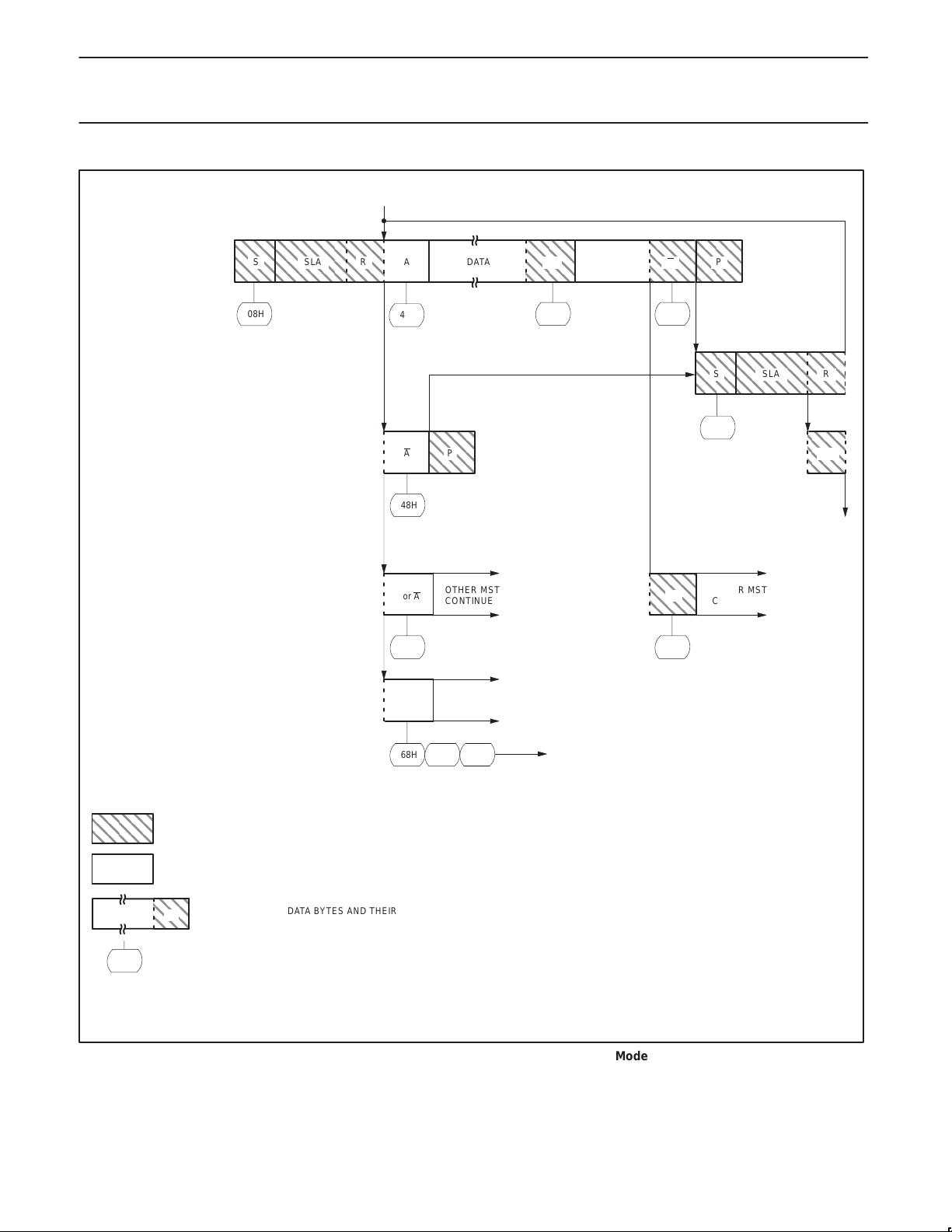
Philips Semiconductors Preliminary specification
ÇÇÇ
80C51 8-bit microcontroller
16K/512 OTP/ROM/ROMless, 8 channel 10 bit A/D, I2C, PWM,
80C554/83C554/87C554
capture/compare, high I/O
MR
SUCCESSFUL RECEPTION
FROM A SLAVE TRANSMITTER
NEXT TRANSFER STARTED WITH A
REPEATED START CONDITION
NOT ACKNOWLEDGE RECEIVED
AFTER THE SLAVE ADDRESS
ARBITRATION LOST IN SLAVE ADDRESS
OR ACKNOWLEDGE BIT
ARBITRATION LOST AND ADDRESSED AS SLAVE
S SLA RA DATA P
08H
40H
A P
48H
A or A
38H
A
OTHER MST
CONTINUES
OTHER MST
CONTINUES
A
50H
DATA
A
58H
A
38H
S SLA R
10H
TO MST/TRX MODE
ENTRY = MT
OTHER MST
CONTINUES
W
DATA A
n
1999 Apr 07
68H 78H 80H
FROM MASTER TO SLAVE
FROM SLAVE TO MASTER
ANY NUMBER OF DATA BYTES AND THEIR ASSOCIATED ACKNOWLEDGE BITS
THIS NUMBER (CONTAINED IN S1STA) CORRESPONDS TO A DEFINED STATE OF THE I
Figure 41. Format and States in the Master Receiver Mode
41
TO CORRESPONDING
STATES IN SLAVE MODE
2
C BUS. SEE TABLE 7.
SU00972
Page 42
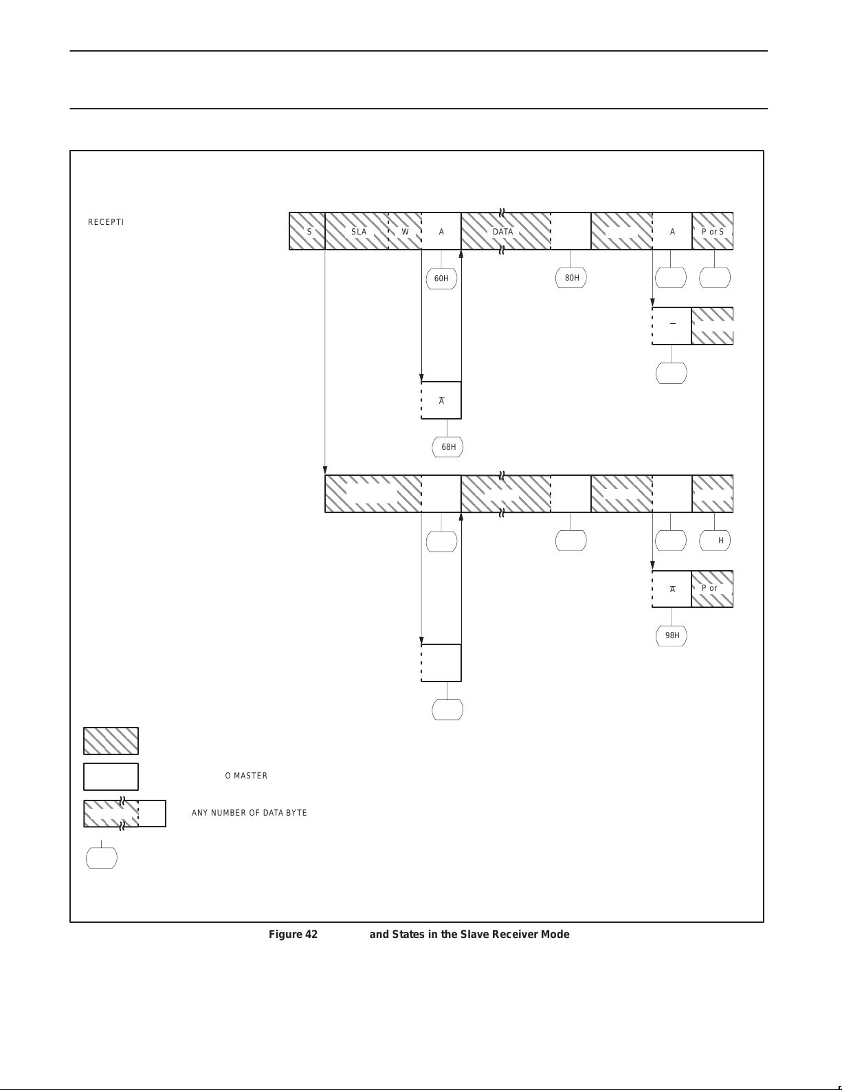
Philips Semiconductors Preliminary specification
ÇÇÇ
ÇÇÇ
ÇÇÇ
80C51 8-bit microcontroller
16K/512 OTP/ROM/ROMless, 8 channel 10 bit A/D, I2C, PWM,
80C554/83C554/87C554
capture/compare, high I/O
RECEPTION OF THE OWN SLAVE ADDRESS
AND ONE OR MORE DATA BYTES
ALL ARE ACKNOWLEDGED.
S SLA WA ADATA P or S
A SLA
DATA
LAST DATA BYTE RECEIVED IS
NOT ACKNOWLEDGED
ARBITRATION LOST AS MST AND
ADDRESSED AS SLAVE
RECEPTION OF THE GENERAL CALL ADDRESS
AND ONE OR MORE DATA BYTES
LAST DATA BYTE IS NOT ACKNOWLEDGED
ARBITRATION LOST AS MST AND ADDRESSED AS SLAVE BY GENERAL CALL
GENERAL
CALL
60H
A
68H
AA
70H
A
DATA P or S
80H
A
90H
DATA
80H A0H
P or S
A
88H
90H A0H
P or S
A
98H
Data
n
1999 Apr 07
78H
FROM MASTER TO SLAVE
FROM SLAVE TO MASTER
A
ANY NUMBER OF DATA BYTES AND THEIR ASSOCIATED ACKNOWLEDGE BITS
THIS NUMBER (CONTAINED IN S1STA) CORRESPONDS TO A DEFINED STATE OF THE I
Figure 42. Format and States in the Slave Receiver Mode
42
2
C BUS. SEE TABLE 8.
SU00973
Page 43
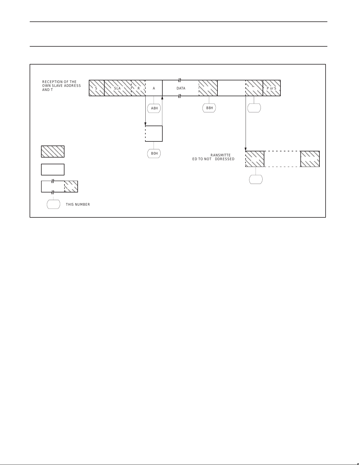
Philips Semiconductors Preliminary specification
80C51 8-bit microcontroller
16K/512 OTP/ROM/ROMless, 8 channel 10 bit A/D, I2C, PWM,
80C554/83C554/87C554
capture/compare, high I/O
RECEPTION OF THE
OWN SLAVE ADDRESS
AND TRANSMISSION
OF ONE OR MORE
DATA BYTES
S SLA RA DATA P or S
ADATAA
A8H
A
FROM MASTER TO SLAVE
FROM SLAVE TO MASTER
DATA
A
ANY NUMBER OF DATA BYTES AND THEIR ASSOCIATED ACKNOWLEDGE BITS
n
THIS NUMBER (CONTAINED IN S1STA) CORRESPONDS TO A DEFINED STATE OF THE I
B0H
Figure 43. Format and States of the Slave Transmitter Mode
B8H
ARBITRATION LOAST AS MST
AND ADDRESSED AS SLAVE
LAST DATA BYTE TRANSMITTED.
SWITCHED TO NOT ADDRESSED
SLAVE (AA BIT IN S1CON = “0”
2
C BUS. SEE TABLE 9.
C0H
C8H
A
All “1”s
P or S
SU00974
1999 Apr 07
43
Page 44

Philips Semiconductors Preliminary specification
STATUS
STATUS OF THE
(S1STA)
SIO1 HARDWARE
TO/FROM S1DAT
80C51 8-bit microcontroller
16K/512 OTP/ROM/ROMless, 8 channel 10 bit A/D, I2C, PWM,
80C554/83C554/87C554
capture/compare, high I/O
Table 6. Master Transmitter Mode
APPLICATION SOFTWARE RESPONSE
CODE
08H A START condition has
10H A repeated START
18H SLA+W has been
20H SLA+W has been
28H Data byte in S1DAT has
30H Data byte in S1DAT has
38H Arbitration lost in
I2C BUS AND
been transmitted
condition has been
transmitted
transmitted; ACK has
been received
transmitted; NOT ACK
has been received
been transmitted; ACK
has been received
been transmitted; NOT
ACK has been received
SLA+R/W or
Data bytes
TO S1CON
STA STO SI AA
Load SLA+W X 0 0 X SLA+W will be transmitted;
Load SLA+W or X 0 0 X As above
Load SLA+R X 0 0 X SLA+W will be transmitted;
Load data byte or 0 0 0 X Data byte will be transmitted;
no S1DAT action or 1 0 0 X Repeated START will be transmitted;
no S1DAT action or 0 1 0 X STOP condition will be transmitted;
no S1DAT action 1 1 0 X STOP condition followed by a
Load data byte or 0 0 0 X Data byte will be transmitted;
no S1DAT action or 1 0 0 X Repeated START will be transmitted;
no S1DAT action or 0 1 0 X STOP condition will be transmitted;
no S1DAT action 1 1 0 X STOP condition followed by a
Load data byte or 0 0 0 X Data byte will be transmitted;
no S1DAT action or 1 0 0 X Repeated START will be transmitted;
no S1DAT action or 0 1 0 X STOP condition will be transmitted;
no S1DAT action 1 1 0 X STOP condition followed by a
Load data byte or 0 0 0 X Data byte will be transmitted;
no S1DAT action or 1 0 0 X Repeated START will be transmitted;
no S1DAT action or 0 1 0 X STOP condition will be transmitted;
no S1DAT action 1 1 0 X STOP condition followed by a
No S1DAT action or 0 0 0 X I2C bus will be released;
No S1DAT action 1 0 0 X A START condition will be transmitted when the
NEXT ACTION TAKEN BY SIO1 HARDWARE
ACK bit will be received
SIO1 will be switched to MST/REC mode
ACK bit will be received
STO flag will be reset
STAR T condition will be transmitted;
STO flag will be reset
ACK bit will be received
STO flag will be reset
STAR T condition will be transmitted;
STO flag will be reset
ACK bit will be received
STO flag will be reset
STAR T condition will be transmitted;
STO flag will be reset
ACK bit will be received
STO flag will be reset
STAR T condition will be transmitted;
STO flag will be reset
not addressed slave will be entered
bus becomes free
1999 Apr 07
44
Page 45

Philips Semiconductors Preliminary specification
2
STATUS
STATUS OF THE I C
(S1STA)
SIO1 HARDWARE
TO/FROM S1DAT
80C51 8-bit microcontroller
16K/512 OTP/ROM/ROMless, 8 channel 10 bit A/D, I2C, PWM,
80C554/83C554/87C554
capture/compare, high I/O
Table 7. Master Receiver Mode
APPLICATION SOFTWARE RESPONSE
CODE
08H A STAR T condition has
10H A repeated STAR T
38H Arbitration lost in
40H SLA+R has been
48H SLA+R has been
50H Data byte has been
58H Data byte has been
BUS AND
been transmitted
condition has been
transmitted
NOT ACK bit
transmitted; ACK has
been received
transmitted; NOT ACK
has been received
received; ACK has been
returned
received; NOT ACK has
been returned
TO S1CON
STA STO SI AA
Load SLA+R X 0 0 X SLA+R will be transmitted;
Load SLA+R or X 0 0 X As above
Load SLA+W X 0 0 X SLA+W will be transmitted;
No S1DAT action or 0 0 0 X I2C bus will be released;
No S1DAT action 1 0 0 X A ST AR T condition will be transmitted when the
No S1DAT action or 0 0 0 0 Data byte will be received;
no S1DAT action 0 0 0 1 Data byte will be received;
No S1DAT action or 1 0 0 X Repeated START condition will be transmitted
no S1DAT action or 0 1 0 X STOP condition will be transmitted;
no S1DAT action 1 1 0 X STOP condition followed by a
Read data byte or 0 0 0 0 Data byte will be received;
read data byte 0 0 0 1 Data byte will be received;
Read data byte or 1 0 0 X Repeated START condition will be transmitted
read data byte or 0 1 0 X STOP condition will be transmitted;
read data byte 1 1 0 X STOP condition followed by a
NEXT ACTION TAKEN BY SIO1 HARDWARE
ACK bit will be received
SIO1 will be switched to MST/TRX mode
SIO1 will enter a slave mode
bus becomes free
NOT ACK bit will be returned
ACK bit will be returned
STO flag will be reset
STAR T condition will be transmitted;
STO flag will be reset
NOT ACK bit will be returned
ACK bit will be returned
STO flag will be reset
STAR T condition will be transmitted;
STO flag will be reset
1999 Apr 07
45
Page 46

Philips Semiconductors Preliminary specification
STATUS
STATUS OF THE
(S1STA)
SIO1 HARDWARE
TO/FROM S1DAT
received ACK has
has been received
80C51 8-bit microcontroller
16K/512 OTP/ROM/ROMless, 8 channel 10 bit A/D, I2C, PWM,
80C554/83C554/87C554
capture/compare, high I/O
Table 8. Slave Receiver Mode
APPLICATION SOFTWARE RESPONSE
CODE
60H Own SLA+W has
68H Arbitration lost in
70H General call address
78H Arbitration lost in
80H Previously addressed
88H Previously addressed
90H Previously addressed
98H Previously addressed
I2C BUS AND
been received; ACK
has been returned
SLA+R/W as master;
Own SLA+W has
been received, ACK
returned
(00H) has been
;
been returned
SLA+R/W as master;
General call address
,
ACK has been
returned
with own SLV
address; DATA has
been received; ACK
has been returned
with own SLA; DATA
byte has been
received; NOT ACK
has been returned
with General Call;
DATA byte has been
received; ACK has
been returned
with General Call;
DATA byte has been
received; NOT ACK
has been returned
TO S1CON
STA STO SI AA
No S1DAT action or X 0 0 0 Data byte will be received and NOT ACK will be
no S1DAT action X 0 0 1 Data byte will be received and ACK will be returned
No S1DAT action or X 0 0 0 Data byte will be received and NOT ACK will be
no S1DAT action X 0 0 1 Data byte will be received and ACK will be returned
No S1DAT action or X 0 0 0 Data byte will be received and NOT ACK will be
no S1DAT action X 0 0 1 Data byte will be received and ACK will be returned
No S1DAT action or X 0 0 0 Data byte will be received and NOT ACK will be
no S1DAT action X 0 0 1 Data byte will be received and ACK will be returned
Read data byte or X 0 0 0 Data byte will be received and NOT ACK will be
read data byte X 0 0 1 Data byte will be received and ACK will be returned
Read data byte or 0 0 0 0 Switched to not addressed SLV mode; no recognition
read data byte or 0 0 0 1 Switched to not addressed SLV mode; Own SLA will
read data byte or 1 0 0 0 Switched to not addressed SLV mode; no recognition
read data byte 1 0 0 1 Switched to not addressed SLV mode; Own SLA will
Read data byte or X 0 0 0 Data byte will be received and NOT ACK will be
read data byte X 0 0 1 Data byte will be received and ACK will be returned
Read data byte or 0 0 0 0 Switched to not addressed SLV mode; no recognition
read data byte or 0 0 0 1 Switched to not addressed SLV mode; Own SLA will
read data byte or 1 0 0 0 Switched to not addressed SLV mode; no recognition
read data byte 1 0 0 1 Switched to not addressed SLV mode; Own SLA will
NEXT ACTION TAKEN BY SIO1 HARDWARE
returned
returned
returned
returned
returned
of own SLA or General call address
be recognized; General call address will be
recognized if S1ADR.0 = logic 1
of own SLA or General call address. A START
condition will be transmitted when the bus becomes
free
be recognized; General call address will be
recognized if S1ADR.0 = logic 1. A START condition
will be transmitted when the bus becomes free.
returned
of own SLA or General call address
be recognized; General call address will be
recognized if S1ADR.0 = logic 1
of own SLA or General call address. A START
condition will be transmitted when the bus becomes
free
be recognized; General call address will be
recognized if S1ADR.0 = logic 1. A START condition
will be transmitted when the bus becomes free.
1999 Apr 07
46
Page 47
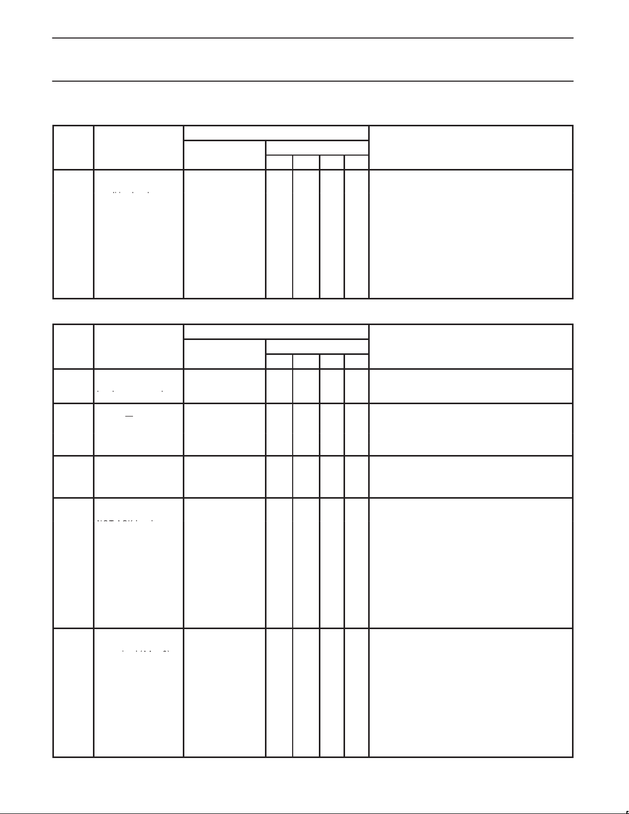
Philips Semiconductors Preliminary specification
STATUS
STATUS OF THE
(S1STA)
SIO1 HARDWARE
TO/FROM S1DAT
SLV/REC
SLV/TRX
STATUS
STATUS OF THE
(S1STA)
SIO1 HARDWARE
TO/FROM S1DAT
ACK has been
80C51 8-bit microcontroller
16K/512 OTP/ROM/ROMless, 8 channel 10 bit A/D, I2C, PWM,
80C554/83C554/87C554
capture/compare, high I/O
Table 8. Slave Receiver Mode (Continued)
APPLICATION SOFTWARE RESPONSE
CODE
A0H A STOP condition or
Table 9. Slave Transmitter Mode
CODE
A8H Own SLA+R has
B0H Arbitration lost in
B8H Data byte in S1DAT
C0H Data byte in S1DA T
C8H Last data byte in
I2C BUS AND
repeated STAR T
condition has been
received while still
addressed as
or
I2C BUS AND
been received; ACK
has been returned
SLA+R/W as master;
Own SLA+R has
been received, ACK
has been returned
has been transmitted;
received
has been transmitted;
NOT ACK has been
received
S1DAT has been
transmitted (AA = 0);
ACK has been
received
TO S1CON
STA STO SI AA
No STDAT action or 0 0 0 0 Switched to not addressed SLV mode; no recognition
No STDAT action or 0 0 0 1 Switched to not addressed SLV mode; Own SLA will
No STDAT action or 1 0 0 0 Switched to not addressed SLV mode; no recognition
No STDAT action 1 0 0 1 Switched to not addressed SLV mode; Own SLA will
APPLICATION SOFTWARE RESPONSE
TO S1CON
STA STO SI AA
Load data byte or X 0 0 0 Last data byte will be transmitted and ACK bit will be
load data byte X 0 0 1 Data byte will be transmitted; ACK will be received
Load data byte or X 0 0 0 Last data byte will be transmitted and ACK bit will be
load data byte X 0 0 1 Data byte will be transmitted; ACK bit will be received
Load data byte or X 0 0 0 Last data byte will be transmitted and ACK bit will be
load data byte X 0 0 1 Data byte will be transmitted; ACK bit will be received
No S1DAT action or 0 0 0 01 Switched to not addressed SLV mode; no recognition
no S1DAT action or 0 0 0 1 Switched to not addressed SLV mode; Own SLA will
no S1DAT action or 1 0 0 0 Switched to not addressed SLV mode; no recognition
no S1DAT action 1 0 0 1 Switched to not addressed SLV mode; Own SLA will
No S1DAT action or 0 0 0 0 Switched to not addressed SLV mode; no recognition
no S1DAT action or 0 0 0 1 Switched to not addressed SLV mode; Own SLA will
no S1DAT action or 1 0 0 0 Switched to not addressed SLV mode; no recognition
no S1DAT action 1 0 0 1 Switched to not addressed SLV mode; Own SLA will
NEXT ACTION TAKEN BY SIO1 HARDWARE
of own SLA or General call address
be recognized; General call address will be
recognized if S1ADR.0 = logic 1
of own SLA or General call address. A START
condition will be transmitted when the bus becomes
free
be recognized; General call address will be
recognized if S1ADR.0 = logic 1. A START condition
will be transmitted when the bus becomes free.
NEXT ACTION TAKEN BY SIO1 HARDWARE
received
received
received
of own SLA or General call address
be recognized; General call address will be
recognized if S1ADR.0 = logic 1
of own SLA or General call address. A START
condition will be transmitted when the bus becomes
free
be recognized; General call address will be
recognized if S1ADR.0 = logic 1. A START condition
will be transmitted when the bus becomes free.
of own SLA or General call address
be recognized; General call address will be
recognized if S1ADR.0 = logic 1
of own SLA or General call address. A START
condition will be transmitted when the bus becomes
free
be recognized; General call address will be
recognized if S1ADR.0 = logic 1. A START condition
will be transmitted when the bus becomes free.
1999 Apr 07
47
Page 48
Philips Semiconductors Preliminary specification
STATUS
STATUS OF THE
(S1STA)
SIO1 HARDWARE
TO/FROM S1DAT
80C51 8-bit microcontroller
16K/512 OTP/ROM/ROMless, 8 channel 10 bit A/D, I2C, PWM,
80C554/83C554/87C554
capture/compare, high I/O
Table 10. Miscellaneous States
APPLICATION SOFTWARE RESPONSE
CODE
F8H No relevant state
00H Bus error during MST
I2C BUS AND
information available;
SI = 0
or selected slave
modes, due to an
illegal STAR T or
STOP condition. State
00H can also occur
when interference
causes SIO1 to enter
an undefined state.
TO S1CON
NEXT ACTION TAKEN BY SIO1 HARDWARE
STA STO SI AA
No S1DAT action No S1CON action Wait or proceed current transfer
No S1DAT action 0 1 0 X Only the internal hardware is affected in the MST or
addressed SLV modes. In all cases, the bus is
released and SIO1 is switched to the not addressed
SLV mode. STO is reset.
Slave Transmitter Mode: In the slave transmitter mode, a number
of data bytes are transmitted to a master receiver (see Figure 43).
Data transfer is initialized as in the slave receiver mode. When
S1ADR and S1CON have been initialized, SIO1 waits until it is
addressed by its own slave address followed by the data direction
bit which must be “1” (R) for SIO1 to operate in the slave transmitter
mode. After its own slave address and the R bit have been received,
the serial interrupt flag (SI) is set and a valid status code can be
read from S1ST A. This status code is used to vector to an interrupt
service routine, and the appropriate action to be taken for each of
these status codes is detailed in Table 9. The slave transmitter mode
may also be entered if arbitration is lost while SIO1 is in the master
mode (see state B0H).
If the AA bit is reset during a transfer, SIO1 will transmit the last byte
of the transfer and enter state C0H or C8H. SIO1 is switched to the
not addressed slave mode and will ignore the master receiver if it
continues the transfer. Thus the master receiver receives all 1s as
serial data. While AA is reset, SIO1 does not respond to its own
slave address or a general call address. However, the I
2
C bus is still
monitored, and address recognition may be resumed at any time by
setting AA. This means that the AA bit may be used to temporarily
isolate SIO1 from the I
2
C bus.
Miscellaneous States: There are two S1STA codes that do not
correspond to a defined SIO1 hardware state (see Table 10). These
are discussed below.
S1STA = F8H:
This status code indicates that no relevant information is available
because the serial interrupt flag, SI, is not yet set. This occurs
between other states and when SIO1 is not involved in a serial
transfer.
S1STA = 00H:
This status code indicates that a bus error has occurred during an
SIO1 serial transfer. A bus error is caused when a START or STOP
condition occurs at an illegal position in the format frame. Examples
of such illegal positions are during the serial transfer of an address
byte, a data byte, or an acknowledge bit. A bus error may also be
caused when external interference disturbs the internal SIO1
signals. When a bus error occurs, SI is set. To recover from a bus
error, the ST O flag must be set and SI must be cleared. This causes
SIO1 to enter the “not addressed” slave mode (a defined state) and
to clear the STO flag (no other bits in S1CON are affected). The
SDA and SCL lines are released (a STOP condition is not
transmitted).
Some Special Cases: The SIO1 hardware has facilities to handle
the following special cases that may occur during a serial transfer:
Simultaneous Repeated START Conditions from Two Masters
A repeated STAR T condition may be generated in the master
transmitter or master receiver modes. A special case occurs if
another master simultaneously generates a repeated STAR T
condition (see Figure 44). Until this occurs, arbitration is not lost by
either master since they were both transmitting the same data.
If the SIO1 hardware detects a repeated STAR T condition on the I
2
bus before generating a repeated STAR T condition itself, it will
release the bus, and no interrupt request is generated. If another
master frees the bus by generating a STOP condition, SIO1 will
transmit a normal STAR T condition (state 08H), and a retry of the
total serial data transfer can commence.
D
ATA TRANSFER AFTER LOSS OF ARBITRATION
Arbitration may be lost in the master transmitter and master receiver
modes (see Figure 36). Loss of arbitration is indicated by the
following states in S1STA; 38H, 68H, 78H, and B0H (see Figures 40
and 41).
If the STA flag in S1CON is set by the routines which service these
states, then, if the bus is free again, a STAR T condition (state 08H)
is transmitted without intervention by the CPU, and a retry of the
total serial transfer can commence.
F
ORCED ACCESS TO THE I
2
C BUS
In some applications, it may be possible for an uncontrolled source
to cause a bus hang-up. In such situations, the problem may be
caused by interference, temporary interruption of the bus or a
temporary short-circuit between SDA and SCL.
If an uncontrolled source generates a superfluous STAR T or masks
a STOP condition, then the I
2
C bus stays busy indefinitely. If the
STA flag is set and bus access is not obtained within a reasonable
amount of time, then a forced access to the I2C bus is possible. This
is achieved by setting the STO flag while the STA flag is still set. No
STOP condition is transmitted. The SIO1 hardware behaves as if a
STOP condition was received and is able to transmit a START
condition. The STO flag is cleared by hardware (see Figure 45).
C
1999 Apr 07
48
Page 49
Philips Semiconductors Preliminary specification
80C51 8-bit microcontroller
16K/512 OTP/ROM/ROMless, 8 channel 10 bit A/D, I2C, PWM,
80C554/83C554/87C554
capture/compare, high I/O
S
08H
SLA W A DATA A S
18H 28H 08H
OTHER MASTER SENDS REPEATED
START CONDITION EARLIER
Figure 44. Simultaneous Repeated START Conditions from 2 Masters
TIME LIMIT
STA FLAG
STO FLAG
SDA LINE
OTHER MST
CONTINUES
P S SLA
RETRY
SU00975
SCL LINE
Figure 45. Forced Access to a Busy I2C Bus
I2C BUS OBSTRUCTED BY A LOW LEVEL ON SCL OR SDA
2
An I
C bus hang-up occurs if SDA or SCL is pulled LOW by an
uncontrolled source. If the SCL line is obstructed (pulled LOW) by a
device on the bus, no further serial transfer is possible, and the
SIO1 hardware cannot resolve this type of problem. When this
occurs, the problem must be resolved by the device that is pulling
the SCL bus line LOW.
If the SDA line is obstructed by another device on the bus (e.g., a
slave device out of bit synchronization), the problem can be solved
by transmitting additional clock pulses on the SCL line (see Figure
46). The SIO1 hardware transmits additional clock pulses when the
STA flag is set, but no START condition can be generated because
the SDA line is pulled LOW while the I
2
C bus is considered free.
The SIO1 hardware attempts to generate a STAR T condition after
every two additional clock pulses on the SCL line. When the SDA
line is eventually released, a normal STAR T condition is transmitted,
state 08H is entered, and the serial transfer continues.
If a forced bus access occurs or a repeated START condition is
transmitted while SDA is obstructed (pulled LOW), the SIO1
START CONDITION
SU00976
hardware performs the same action as described above. In each
case, state 08H is entered after a successful START condition is
transmitted and normal serial transfer continues. Note that the CPU
is not involved in solving these bus hang-up problems.
B
US ERROR
A bus error occurs when a START or STOP condition is present at
an illegal position in the format frame. Examples of illegal positions
are during the serial transfer of an address byte, a data or an
acknowledge bit.
The SIO1 hardware only reacts to a bus error when it is involved in
a serial transfer either as a master or an addressed slave. When a
bus error is detected, SIO1 immediately switches to the not
addressed slave mode, releases the SDA and SCL lines, sets the
interrupt flag, and loads the status register with 00H. This status
code may be used to vector to a service routine which either
attempts the aborted serial transfer again or simply recovers from
the error condition as shown in Table 10.
1999 Apr 07
49
Page 50
Philips Semiconductors Preliminary specification
80C51 8-bit microcontroller
16K/512 OTP/ROM/ROMless, 8 channel 10 bit A/D, I2C, PWM,
80C554/83C554/87C554
capture/compare, high I/O
STA FLAG
(2) (3)
SDA LINE
SCL LINE
(1) (1)
(1) Unsuccessful attempt to send a Start condition
(2) SDA line released
(3) Successful attempt to send a Start condition; state 08H is entered
Figure 46. Recovering from a Bus Obstruction Caused by a Low Level on SDA
Software Examples of SIO1 Service Routines: This section
consists of a software example for:
– Initialization of SIO1 after a RESET
– Entering the SIO1 interrupt routine
– The 26 state service routines for the
– Master transmitter mode
– Master receiver mode
– Slave receiver mode
– Slave transmitter mode
I
NITIALIZATION
In the initialization routine, SIO1 is enabled for both master and
slave modes. For each mode, a number of bytes of internal data
RAM are allocated to the SIO to act as either a transmission or
reception buffer. In this example, 8 bytes of internal data RAM are
reserved for different purposes. The data memory map is shown in
Figure 47. The initialization routine performs the following functions:
– S1ADR is loaded with the part’ s own slave address and the
general call bit (GC)
– P1.6 and P1.7 bit latches are loaded with logic 1s
– RAM location HADD is loaded with the high-order address byte of
the service routines
– The SIO1 interrupt enable and interrupt priority bits are set
– The slave mode is enabled by simultaneously setting the ENS1
and AA bits in S1CON and the serial clock frequency (for master
modes) is defined by loading CR0 and CR1 in S1CON. The
master routines must be started in the main program.
2
The SIO1 hardware now begins checking the I
C bus for its own
slave address and general call. If the general call or the own slave
address is detected, an interrupt is requested and S1STA is loaded
with the appropriate state information. The following text describes a
fast method of branching to the appropriate service routine.
START CONDITION
SU00977
SIO
1 INTERRUPT ROUTINE
When the SIO1 interrupt is entered, the PSW is first pushed on the
stack. Then S1STA and HADD (loaded with the high-order address
byte of the 26 service routines by the initialization routine) are
pushed on to the stack. S1STA contains a status code which is the
lower byte of one of the 26 service routines. The next instruction is
RET, which is the return from subroutine instruction. When this
instruction is executed, the high and low order address bytes are
popped from stack and loaded into the program counter.
The next instruction to be executed is the first instruction of the state
service routine. Seven bytes of program code (which execute in
eight machine cycles) are required to branch to one of the 26 state
service routines.
SI PUSH PSW Save PSW
PUSH S1STA Push status code
(low order address byte)
PUSH HADD Push high order address byte
RET Jump to state service routine
The state service routines are located in a 256-byte page of program
memory. The location of this page is defined in the initialization
routine. The page can be located anywhere in program memory by
loading data RAM register HADD with the page number. Page 01 is
chosen in this example, and the service routines are located
between addresses 0100H and 01FFH.
T
HE STATE SERVICE ROUTINES
The state service routines are located 8 bytes from each other. Eight
bytes of code are sufficient for most of the service routines. A few of
the routines require more than 8 bytes and have to jump to other
locations to obtain more bytes of code. Each state routine is part of
the SIO1 interrupt routine and handles one of the 26 states. It ends
with a RETI instruction which causes a return to the main program.
1999 Apr 07
50
Page 51
Philips Semiconductors Preliminary specification
80C51 8-bit microcontroller
16K/512 OTP/ROM/ROMless, 8 channel 10 bit A/D, I2C, PWM,
80C554/83C554/87C554
capture/compare, high I/O
SPECIAL FUNCTION REGISTERS
DBS1ADR GC
S1DAT
S1STA
S1CON
0
AAST0STACR2 ENS1
DA
00
D9
CR0CR!SI
D8
PSW
IPO B8
IEN0 AB
P1 90
P1.7 P1.6
INTERNAL DATA RAM
ORIGINAL VALUE OF NUMBYTMST
NUMBYTMST
HADD HIGHER ADDRESS BYTE INTERRUPT ROUTINE
NUMBER OF BYTES AS MASTER
SLA SLA+R/W TO BE TRANSMITTED TO SLA
SLAVE TRANSMITTER DATA RAM
STD
SLAVE RECEIVER DATA RAM
SRD
MASTER RECEIVER DATA RAM
MRD
MASTER TRANSMITTER DATA RAM
MTD
PS1
ES1EA
D0
80
7F
53BACKUP
52
51
50
4F
48
40
38
30
1999 Apr 07
R1
R0
Figure 47. SIO1 Data Memory Map
51
19
18
00
SU00978
Page 52

Philips Semiconductors Preliminary specification
80C51 8-bit microcontroller
16K/512 OTP/ROM/ROMless, 8 channel 10 bit A/D, I2C, PWM,
80C554/83C554/87C554
capture/compare, high I/O
ASTER TRANSMITTER AND MASTER RECEIVER MODES
M
The master mode is entered in the main program. To enter the
master transmitter mode, the main program must first load the
internal data RAM with the slave address, data bytes, and the
number of data bytes to be transmitted. To enter the master receiver
mode, the main program must first load the internal data RAM with
the slave address and the number of data bytes to be received. The
R/W
bit determines whether SIO1 operates in the master transmitter
or master receiver mode.
Master mode operation commences when the STA bit in S1CION is
set by the SETB instruction and data transfer is controlled by the
master state service routines in accordance with Table 6, Table 7,
Figure 40, and Figure 41. In the example below, 4 bytes are
transferred. There is no repeated STAR T condition. In the event of
lost arbitration, the transfer is restarted when the bus becomes free.
If a bus error occurs, the I
not selected slave receiver mode. If a slave device returns a not
acknowledge, a STOP condition is generated.
A repeated STAR T condition can be included in the serial transfer if
the STA flag is set instead of the STO flag in the state service
routines vectored to by status codes 28H and 58H. Additional
software must be written to determine which data is transferred after
a repeated STAR T condition.
LAVE TRANSMITTER AND SLAVE RECEIVER MODES
S
After initialization, SIO1 continually tests the I2C bus and branches
to one of the slave state service routines if it detects its own slave
address or the general call address (see Table 8, Table 9, Figure 42,
and Figure 43). If arbitration was lost while in the master mode, the
master mode is restarted after the current transfer. If a bus error
occurs, the I
2
C bus is released and SIO1 enters the not selected
slave receiver mode.
In the slave receiver mode, a maximum of 8 received data bytes can
be stored in the internal data RAM. A maximum of 8 bytes ensures
that other RAM locations are not overwritten if a master sends more
bytes. If more than 8 bytes are transmitted, a not acknowledge is
returned, and SIO1 enters the not addressed slave receiver mode. A
maximum of one received data byte can be stored in the internal
data RAM after a general call address is detected. If more than one
byte is transmitted, a not acknowledge is returned and SIO1 enters
the not addressed slave receiver mode.
In the slave transmitter mode, data to be transmitted is obtained
from the same locations in the internal data RAM that were
previously loaded by the main program. After a not acknowledge
has been returned by a master receiver device, SIO1 enters the not
addressed slave mode.
DAPTING THE SOFTWARE FOR DIFFERENT APPLICATIONS
A
The following software example shows the typical structure of the
interrupt routine including the 26 state service routines and may be
used as a base for user applications. If one or more of the four
modes are not used, the associated state service routines may be
removed but, care should be taken that a deleted routine can never
be invoked.
This example does not include any time-out routines. In the slave
modes, time-out routines are not very useful since, in these modes,
SIO1 behaves essentially as a passive device. In the master modes,
an internal timer may be used to cause a time-out if a serial transfer
is not complete after a defined period of time. This time period is
defined by the system connected to the I
2
C bus is released and SIO1 enters the
2
C bus.
1999 Apr 07
52
Page 53

Philips Semiconductors Preliminary specification
80C51 8-bit microcontroller
16K/512 OTP/ROM/ROMless, 8 channel 10 bit A/D, I2C, PWM,
80C554/83C554/87C554
capture/compare, high I/O
!********************************************************************************************************
! SI01 EQUATE LIST
!********************************************************************************************************
!********************************************************************************************************
! LOCATIONS OF THE SI01 SPECIAL FUNCTION REGISTERS
00D8 S1CON –0xd8
00D9 S1STA –0xd9
00DA S1DAT –0xda
00DB S1ADR –0xdb
00A8 IEN0 –0xa8
00B8 IP0 –02b8
00DD STA –0xdd ! STA bit in S1CON
00BD SI01HP –0xbd ! IP0, SI01 Priority bit
00D5 ENS1_NOTSTA_STO_NOTSI_AA_CR0 –0xd5 ! Generates STOP
00C5 ENS1_NOTSTA_NOTSTO_NOTSI_AA_CR0 –0xc5 ! Releases BUS and
00C1 ENS1_NOTSTA_NOTSTO_NOTSI_NOTAA_CR0 –0xc1 ! Releases BUS and
00E5 ENS1_STA_NOTSTO_NOTSI_AA_CR0 –0xe5 ! Releases BUS and
!********************************************************************************************************
!********************************************************************************************************
! BIT LOCATIONS
!********************************************************************************************************
!********************************************************************************************************
! IMMEDIATE DATA TO WRITE INTO REGISTER S1CON
!********************************************************************************************************
! (CR0 = 100kHz)
! ACK
! NOT ACK
! set STA
!********************************************************************************************************
! GENERAL IMMEDIATE DATA
0031 OWNSLA –0x31 ! Own SLA+General Call
00A0 ENSI01 –0xa0 ! EA+ES1, enable SIO1 interrupt
0001 PAG1 –0x01 ! select PAG1 as HADD
00C0 SLAW –0xc0 ! SLA+W to be transmitted
00C1 SLAR –0xc1 ! SLA+R to be transmitted
0018 SELRB3 –0x18 ! Select Register Bank 3
0030 MTD –0x30 ! MST/TRX/DATA base address
0038 MRD –0x38 ! MST/REC/DA TA base address
0040 SRD –0x40 ! SLV/REC/DATA base address
0048 STD –0x48 ! SLV/TRX/DATA base address
0053 BACKUP –0x53 ! Backup from NUMBYTMST
0052 NUMBYTMST –0x52 ! Number of bytes to transmit
0051 SLA –0x51 ! Contains SLA+R/W to be
0050 HADD –0x50 ! High Address byte for STATE 0
!********************************************************************************************************
! must be written into S1ADR
! must be written into IEN0
!********************************************************************************************************
! LOCATIONS IN DATA RAM
!********************************************************************************************************
! To restore NUMBYTMST in case
! of an Arbitration Loss.
! or receive as MST.
! transmitted.
! till STATE 25.
1999 Apr 07
53
Page 54

Philips Semiconductors Preliminary specification
80C51 8-bit microcontroller
16K/512 OTP/ROM/ROMless, 8 channel 10 bit A/D, I2C, PWM,
80C554/83C554/87C554
capture/compare, high I/O
!********************************************************************************************************
! INITIALIZATION ROUTINE
! Example to initialize IIC Interface as slave receiver or slave transmitter and
! start a MASTER TRANSMIT or a MASTER RECEIVE function. 4 bytes will be transmitted or received.
!********************************************************************************************************
.sect strt
0000 4100 ajmp INIT ! RESET
0200 75DB31 INIT : mov S1ADR,#OWNSLA ! Load own SLA + enable
0203 D296 setb P1(6) ! P1.6 High level.
0205 D297 setb P1(7) ! P1.7 High level.
0207 755001 mov HADD,#PAG1
020A 43A8A0 orl IEN0,#ENSI01 ! Enable SI01 interrupt
020D C2BD clr SI01HP ! SI01 interrupt low priority
020F 75D8C5 mov S1CON, #ENS1_NOTSTA_NOTSTO_NOTSI_AA_CR0
.base 0x00
.sect initial
.base 0x200
! general call recognition
! Initialize SLV funct.
!********************************************************************************************************
!– – – – – – – – – – – – – – – – – – – – – – – – – – – – – – – – – – – – – – – – – – – – – – – – –
! START MASTER TRANSMIT FUNCTION
!– – – – – – – – – – – – – – – – – – – – – – – – – – – – – – – – – – – – – – – – – – – – – – – – –
0212 755204 mov NUMBYTMST,#0x4 ! Transmit 4 bytes.
0215 7551C0 mov SLA,#SLAW ! SLA+W, T ransmit funct.
0218 D2DD setb STA ! set STA in S1CON
!– – – – – – – – – – – – – – – – – – – – – – – – – – – – – – – – – – – – – – – – – – – – – – – – –
! START MASTER RECEIVE FUNCTION
021A 755204 mov NUMBYTMST,#0x4 ! Receive 4 bytes.
021D 7551C1 mov SLA,#SLAR ! SLA+R, Receive funct.
0220 D2DD setb STA ! set STA in S1CON
002B C0D0 push psw ! save psw
002D C0D9 push S1STA
002F C050 push HADD
0031 22 ret ! JMP to address HADD,S1STA.
!– – – – – – – – – – – – – – – – – – – – – – – – – – – – – – – – – – – – – – – – – – – – – – – – –
!********************************************************************************************************
! SI01 INTERRUPT ROUTINE
!********************************************************************************************************
.sect intvec ! SI01 interrupt vector
.base 0x00
! S1STA and HADD are pushed onto the stack.
! They serve as return address for the RET instruction.
! The RET instruction sets the Program Counter to address HADD,
! S1STA and jumps to the right subroutine.
!– – – – – – – – – – – – – – – – – – – – – – – – – – – – – – – – – – – – – – – – – – – – – – – – –
! STATE : 00, Bus error.
! ACTION : Enter not addressed SLV mode and release bus. STO reset.
!– – – – – – – – – – – – – – – – – – – – – – – – – – – – – – – – – – – – – – – – – – – – – – – – –
.sect st0
.base 0x100
0100 75D8D5 mov S1CON,#ENS1_NOTSTA_STO_NOTSI_AA_CR0 ! clr SI
0103 D0D0 pop psw
0105 32 reti
1999 Apr 07
54
! set STO,AA
Page 55

Philips Semiconductors Preliminary specification
80C51 8-bit microcontroller
16K/512 OTP/ROM/ROMless, 8 channel 10 bit A/D, I2C, PWM,
80C554/83C554/87C554
capture/compare, high I/O
!********************************************************************************************************
!********************************************************************************************************
! MASTER STATE SERVICE ROUTINES
!********************************************************************************************************
! State 08 and State 10 are both for MST/TRX and MST/REC.
! The R/W bit decides whether the next state is within
! MST/TRX mode or within MST/REC mode.
!********************************************************************************************************
!– – – – – – – – – – – – – – – – – – – – – – – – – – – – – – – – – – – – – – – – – – – – – – – – –
! STATE : 08, A, ST AR T condition has been transmitted.
! ACTION : SLA+R/W are transmitted, ACK bit is received.
!– – – – – – – – – – – – – – – – – – – – – – – – – – – – – – – – – – – – – – – – – – – – – – – – –
.sect mts8
.base 0x108
0108 8551DA mov S1DAT,SLA ! Load SLA+R/W
010B 75D8C5 mov S1CON,#ENS1_NOTSTA_NOTSTO_NOTSI_AA_CR0
010E 01A0 ajmp INITBASE1
!– – – – – – – – – – – – – – – – – – – – – – – – – – – – – – – – – – – – – – – – – – – – – – – – –
! STATE : 10, A repeated START condition has been
! transmitted.
! ACTION : SLA+R/W are transmitted, ACK bit is received.
!– – – – – – – – – – – – – – – – – – – – – – – – – – – – – – – – – – – – – – – – – – – – – – – – –
.sect mts10
.base 0x110
! clr SI
0110 8551DA mov S1DAT,SLA ! Load SLA+R/W
0113 75D8C5 mov S1CON,#ENS1_NOTSTA_NOTSTO_NOTSI_AA_CR0
010E 01A0 ajmp INITBASE1
.sect ibase1
.base 0xa0
00A0 75D018 INITBASE1: mov psw,#SELRB3
00A3 7930 mov r1,#MTD
00A5 7838 mov r0,#MRD
00A7 855253 mov BACKUP,NUMBYTMST ! Save initial value
00AA D0D0 pop psw
00AC 32 reti
!********************************************************************************************************
!********************************************************************************************************
! MASTER TRANSMITTER STATE SERVICE ROUTINES
!********************************************************************************************************
!********************************************************************************************************
!– – – – – – – – – – – – – – – – – – – – – – – – – – – – – – – – – – – – – – – – – – – – – – – – –
! STATE : 18, Previous state was STATE 8 or STATE 10, SLA+W have been transmitted,
! ACK has been received.
! ACTION : First DATA is transmitted, ACK bit is received.
!– – – – – – – – – – – – – – – – – – – – – – – – – – – – – – – – – – – – – – – – – – – – – – – – –
.sect mts18
.base 0x118
! clr SI
0118 75D018 mov psw,#SELRB3
011B 87DA mov S1DAT,@r1
011D 01B5 ajmp CON
1999 Apr 07
55
Page 56

Philips Semiconductors Preliminary specification
80C51 8-bit microcontroller
16K/512 OTP/ROM/ROMless, 8 channel 10 bit A/D, I2C, PWM,
80C554/83C554/87C554
capture/compare, high I/O
!– – – – – – – – – – – – – – – – – – – – – – – – – – – – – – – – – – – – – – – – – – – – – – – – –
! STATE : 20, SLA+W have been transmitted, NOT ACK has been received
! ACTION : Transmit STOP condition.
!– – – – – – – – – – – – – – – – – – – – – – – – – – – – – – – – – – – – – – – – – – – – – – – – –
.sect mts20
.base 0x120
0120 75D8D5 mov S1CON,#ENS1_NOTSTA_STO_NOTSI_AA_CR0
0123 D0D0 pop psw
0125 32 reti
!– – – – – – – – – – – – – – – – – – – – – – – – – – – – – – – – – – – – – – – – – – – – – – – – –
! STATE : 28, DATA of S1DAT have been transmitted, ACK received.
! ACTION : If T ransmitted DATA is last DAT A then transmit a STOP condition,
! else transmit next DATA.
!– – – – – – – – – – – – – – – – – – – – – – – – – – – – – – – – – – – – – – – – – – – – – – – – –
.sect mts28
.base 0x128
0128 D55285 djnz NUMBYTMST,NOTLDAT1 ! JMP if NOT last DATA
012B 75D8D5 mov S1CON,#ENS1_NOTSTA_STO_NOTSI_AA_CR0
012E 01B9 ajmp RETmt
.sect mts28sb
.base 0x0b0
00B0 75D018 NOTLDAT1: mov psw,#SELRB3
00B3 87DA mov S1DAT,@r1
00B5 75D8C5 CON: mov S1CON,#ENS1_NOTSTA_NOTSTO_NOTSI_AA_CR0
00B8 09 inc r1
00B9 D0D0 RETmt : pop psw
00BB 32 reti
!– – – – – – – – – – – – – – – – – – – – – – – – – – – – – – – – – – – – – – – – – – – – – – – – –
! STATE : 30, DATA of S1DAT have been transmitted, NOT ACK received.
! ACTION : Transmit a STOP condition.
!– – – – – – – – – – – – – – – – – – – – – – – – – – – – – – – – – – – – – – – – – – – – – – – – –
.sect mts30
.base 0x130
! set STO, clr SI
! clr SI, set AA
! clr SI, set AA
0130 75D8D5 mov S1CON,#ENS1_NOTSTA_STO_NOTSI_AA_CR0
0133 D0D0 pop psw
0135 32 reti
!– – – – – – – – – – – – – – – – – – – – – – – – – – – – – – – – – – – – – – – – – – – – – – – – –
! STATE : 38, Arbitration lost in SLA+W or DATA.
! ACTION : Bus is released, not addressed SLV mode is entered.
! A new START condition is transmitted when the IIC bus is free again.
!– – – – – – – – – – – – – – – – – – – – – – – – – – – – – – – – – – – – – – – – – – – – – – – – –
.sect mts38
.base 0x138
0138 75D8E5 mov S1CON,#ENS1_STA_NOTSTO_NOTSI_AA_CR0
013B 855352 mov NUMBYTMST,BACKUP
013E 01B9 ajmp RETmt
1999 Apr 07
56
! set STO, clr SI
Page 57

Philips Semiconductors Preliminary specification
80C51 8-bit microcontroller
16K/512 OTP/ROM/ROMless, 8 channel 10 bit A/D, I2C, PWM,
80C554/83C554/87C554
capture/compare, high I/O
!********************************************************************************************************
!********************************************************************************************************
! MASTER RECEIVER STATE SERVICE ROUTINES
!********************************************************************************************************
!********************************************************************************************************
!– – – – – – – – – – – – – – – – – – – – – – – – – – – – – – – – – – – – – – – – – – – – – – – – –
! STATE : 40, Previous state was STATE 08 or STATE 10,
! SLA+R have been transmitted, ACK received.
! ACTION : DATA will be received, ACK returned.
!– – – – – – – – – – – – – – – – – – – – – – – – – – – – – – – – – – – – – – – – – – – – – – – – –
.sect mts40
.base 0x140
0140 75D8C5 mov S1CON,#ENS1_NOTSTA_NOTSTO_NOTSI_AA_CR0
0143 D0D0 pop psw
32 reti
!– – – – – – – – – – – – – – – – – – – – – – – – – – – – – – – – – – – – – – – – – – – – – – – – –
! STATE : 48, SLA+R have been transmitted, NOT ACK received.
! ACTION : STOP condition will be generated.
!– – – – – – – – – – – – – – – – – – – – – – – – – – – – – – – – – – – – – – – – – – – – – – – – –
.sect mts48
.base 0x148
0148 75D8D5 STOP: mov S1CON,#ENS1_NOTSTA_STO_NOTSI_AA_CR0
014B D0D0 pop psw
014D 32 reti
!– – – – – – – – – – – – – – – – – – – – – – – – – – – – – – – – – – – – – – – – – – – – – – – – –
! STATE : 50, DATA have been received, ACK returned.
! ACTION : Read DATA of S1DAT.
! DATA will be received, if it is last DATA
then NOT ACK will be returned else ACK will be returned.
!– – – – – – – – – – – – – – – – – – – – – – – – – – – – – – – – – – – – – – – – – – – – – – – – –
.sect mrs50
.base 0x150
0150 75D018 mov psw,#SELRB3
0153 A6DA mov @r0,S1DAT ! Read received DATA
0155 01C0 ajmp REC1
.sect mrs50s
.base 0xc0
! clr STA, STO, SI set AA
! set STO, clr SI
00C0 D55205 REC1: djnz NUMBYTMST,NOTLDAT2
00C3 75D8C1 mov S1CON,#ENS1_NOTSTA_NOTSTO_NOTSI_NOTAA_CR0
00C6 8003 sjmp RETmr
00C8 75D8C5 NOTLDAT2: mov S1CON,#ENS1_NOTSTA_NOTSTO_NOTSI_AA_CR0
00CB 08 RETmr: inc r0
00CC D0D0 pop psw
00CE 32 reti
!– – – – – – – – – – – – – – – – – – – – – – – – – – – – – – – – – – – – – – – – – – – – – – – – –
! STATE : 58, DATA have been received, NOT ACK returned.
! ACTION : Read DATA of S1DAT and generate a STOP condition.
!– – – – – – – – – – – – – – – – – – – – – – – – – – – – – – – – – – – – – – – – – – – – – – – – –
.sect mrs58
.base 0x158
0158 75D018 mov psw,#SELRB3
015B A6DA mov @R0,S1DAT
015D 80E9 sjmp STOP
1999 Apr 07
57
! clr SI,AA
! clr SI, set AA
Page 58

Philips Semiconductors Preliminary specification
80C51 8-bit microcontroller
16K/512 OTP/ROM/ROMless, 8 channel 10 bit A/D, I2C, PWM,
80C554/83C554/87C554
capture/compare, high I/O
!********************************************************************************************************
!********************************************************************************************************
! SLAVE RECEIVER STATE SERVICE ROUTINES
!********************************************************************************************************
!********************************************************************************************************
!– – – – – – – – – – – – – – – – – – – – – – – – – – – – – – – – – – – – – – – – – – – – – – – – –
! STATE : 60, Own SLA+W have been received, ACK returned.
! ACTION : DATA will be received and ACK returned.
!– – – – – – – – – – – – – – – – – – – – – – – – – – – – – – – – – – – – – – – – – – – – – – – – –
.sect srs60
0160 75D8C5 mov S1CON,#ENS1_NOTSTA_NOTSTO_NOTSI_AA_CR0
0163 75D018 mov psw,#SELRB3
0166 01D0 ajmp INITSRD
00D0 7840 INITSRD: mov r0,#SRD
00D2 7908 mov r1,#8
00D4 D0D0 pop psw
00D6 32 reti
.base 0x160
! clr SI, set AA
.sect insrd
.base 0xd0
!– – – – – – – – – – – – – – – – – – – – – – – – – – – – – – – – – – – – – – – – – – – – – – – – –
! STATE : 68, Arbitration lost in SLA and R/W as MST
! Own SLA+W have been received, ACK returned
! ACTION : DATA will be received and ACK returned.
! STA is set to restart MST mode after the bus is free again.
!– – – – – – – – – – – – – – – – – – – – – – – – – – – – – – – – – – – – – – – – – – – – – – – – –
.sect srs68
0168 75D8E5 mov S1CON,#ENS1_STA_NOTSTO_NOTSI_AA_CR0
016B 75D018 mov psw,#SELRB3
016E 01D0 ajmp INITSRD
0170 75D8C5 mov S1CON,#ENS1_NOTSTA_NOTSTO_NOTSI_AA_CR0
0173 75D018 mov psw,#SELRB3 ! Initialize SRD counter
0176 01D0 ajmp initsrd
0178 75D8E5 mov S1CON,#ENS1_STA_NOTSTO_NOTSI_AA_CR0
017B 75D018 mov psw,#SELRB3 ! Initialize SRD counter
017E 01D0 ajmp INITSRD
.base 0x168
!– – – – – – – – – – – – – – – – – – – – – – – – – – – – – – – – – – – – – – – – – – – – – – – – –
! STATE : 70, General call has been received, ACK returned.
! ACTION : DATA will be received and ACK returned.
!– – – – – – – – – – – – – – – – – – – – – – – – – – – – – – – – – – – – – – – – – – – – – – – – –
.sect srs70
.base 0x170
! clr SI, set AA
!– – – – – – – – – – – – – – – – – – – – – – – – – – – – – – – – – – – – – – – – – – – – – – – – –
! STATE : 78, Arbitration lost in SLA+R/W as MST.
! General call has been received, ACK returned.
! ACTION : DATA will be received and ACK returned.
! STA is set to restart MST mode after the bus is free again.
!– – – – – – – – – – – – – – – – – – – – – – – – – – – – – – – – – – – – – – – – – – – – – – – – –
.sect srs78
.base 0x178
1999 Apr 07
58
Page 59

Philips Semiconductors Preliminary specification
80C51 8-bit microcontroller
16K/512 OTP/ROM/ROMless, 8 channel 10 bit A/D, I2C, PWM,
80C554/83C554/87C554
capture/compare, high I/O
!– – – – – – – – – – – – – – – – – – – – – – – – – – – – – – – – – – – – – – – – – – – – – – – – –
! STATE : 80, Previously addressed with own SLA. DATA received, ACK returned.
! ACTION : Read DATA.
! IF received DATA was the last
! THEN superfluous DATA will be received and NOT ACK returned
!– – – – – – – – – – – – – – – – – – – – – – – – – – – – – – – – – – – – – – – – – – – – – – – – –
.sect srs80
.base 0x180
0180 75D018 mov psw,#SELRB3
0183 A6DA mov @r0,S1DAT ! Read received DATA
0185 01D8 ajmp REC2
.sect srs80s
.base 0xd8
00D8 D906 REC2: djnz r1,NOTLDAT3
00DA 75D8C1 LDAT: mov S1CON,#ENS1_NOTSTA_NOTSTO_NOTSI_NOTAA_CR0
00DD D0D0 pop psw
00DF 32 reti
00E0 75D8C5 NOTLDAT3: mov S1CON,#ENS1_NOTSTA_NOTSTO_NOTSI_AA_CR0
00E3 08 inc r0
00E4 D0D0 RETsr: pop psw
00E6 32 reti
ELSE next DATA will be received and ACK returned.
! clr SI,AA
! clr SI, set AA
!– – – – – – – – – – – – – – – – – – – – – – – – – – – – – – – – – – – – – – – – – – – – – – – – –
! STATE : 88, Previously addressed with own SLA. DATA received NOT ACK returned.
! ACTION : No save of DATA, Enter NOT addressed SLV mode.
! Recognition of own SLA. General call recognized, if S1ADR. 0–1.
!– – – – – – – – – – – – – – – – – – – – – – – – – – – – – – – – – – – – – – – – – – – – – – – – –
.sect srs88
.base 0x188
0188 75D8C5 mov S1CON,#ENS1_NOTSTA_NOTSTO_NOTSI_AA_CR0
018B 01E4 ajmp RETsr
!– – – – – – – – – – – – – – – – – – – – – – – – – – – – – – – – – – – – – – – – – – – – – – – – –
! STATE : 90, Previously addressed with general call.
! DATA has been received, ACK has been returned.
! ACTION : Read DATA.
After General call only one byte will be received with ACK
! the second DATA will be received with NOT ACK.
! DATA will be received and NOT ACK returned.
!– – – – – – – – – – – – – – – – – – – – – – – – – – – – – – – – – – – – – – – – – – – – – – – – –
.sect srs90
.base 0x190
0190 75D018 mov psw,#SELRB3
0193 A6DA mov @r0,S1DAT ! Read received DATA
0195 01DA ajmp LDAT
!– – – – – – – – – – – – – – – – – – – – – – – – – – – – – – – – – – – – – – – – – – – – – – – – –
! STATE : 98, Previously addressed with general call.
! DATA has been received, NOT ACK has been returned.
! ACTION : No save of DATA, Enter NOT addressed SLV mode.
Recognition of own SLA. General call recognized, if S1ADR. 0–1.
!– – – – – – – – – – – – – – – – – – – – – – – – – – – – – – – – – – – – – – – – – – – – – – – – –
.sect srs98
.base 0x198
! clr SI, set AA
0198 75D8C5 mov S1CON,#ENS1_NOTSTA_NOTSTO_NOTSI_AA_CR0
019B D0D0 pop psw
019D 32 reti
1999 Apr 07
59
! clr SI, set AA
Page 60

Philips Semiconductors Preliminary specification
80C51 8-bit microcontroller
16K/512 OTP/ROM/ROMless, 8 channel 10 bit A/D, I2C, PWM,
80C554/83C554/87C554
capture/compare, high I/O
!– – – – – – – – – – – – – – – – – – – – – – – – – – – – – – – – – – – – – – – – – – – – – – – – –
! STATE : A0, A STOP condition or repeated START has been received,
! while still addressed as SLV/REC or SLV/TRX.
! ACTION : No save of DATA, Enter NOT addressed SLV mode.
! Recognition of own SLA. General call recognized, if S1ADR. 0–1.
!– – – – – – – – – – – – – – – – – – – – – – – – – – – – – – – – – – – – – – – – – – – – – – – – –
.sect srsA0
.base 0x1a0
01A0 75D8C5 mov S1CON,#ENS1_NOTSTA_NOTSTO_NOTSI_AA_CR0
01A3 D0D0 pop psw
01A5 32 reti
!********************************************************************************************************
!********************************************************************************************************
! SLAVE TRANSMITTER STATE SERVICE ROUTINES
!********************************************************************************************************
!********************************************************************************************************
!– – – – – – – – – – – – – – – – – – – – – – – – – – – – – – – – – – – – – – – – – – – – – – – – –
! STATE : A8, Own SLA+R received, ACK returned.
! ACTION : DATA will be transmitted, A bit received.
!– – – – – – – – – – – – – – – – – – – – – – – – – – – – – – – – – – – – – – – – – – – – – – – – –
.sect stsa8
.base 0x1a8
01A8 8548DA mov S1DAT,STD ! load DATA in S1DAT
01AB 75D8C5 mov S1CON,#ENS1_NOTSTA_NOTSTO_NOTSI_AA_CR0
01AE 01E8 ajmp INITBASE2
.sect ibase2
.base 0xe8
00E8 75D018 INITBASE2: mov psw,#SELRB3
00EB 7948 mov r1, #STD
00ED 09 inc r1
00EE D0D0 pop psw
00F0 32 reti
! clr SI, set AA
! clr SI, set AA
!– – – – – – – – – – – – – – – – – – – – – – – – – – – – – – – – – – – – – – – – – – – – – – – – –
! STATE : B0, Arbitration lost in SLA and R/W as MST. Own SLA+R received, ACK returned.
! ACTION : DATA will be transmitted, A bit received.
! STA is set to restart MST mode after the bus is free again.
!– – – – – – – – – – – – – – – – – – – – – – – – – – – – – – – – – – – – – – – – – – – – – – – – –
.sect stsb0
.base 0x1b0
01B0 8548DA mov S1DAT,STD ! load DATA in S1DAT
01B3 75D8E5 mov S1CON,#ENS1_STA_NOTST O_NOTSI_AA_CR0
01B6 01E8 ajmp INITBASE2
1999 Apr 07
60
Page 61

Philips Semiconductors Preliminary specification
80C51 8-bit microcontroller
16K/512 OTP/ROM/ROMless, 8 channel 10 bit A/D, I2C, PWM,
80C554/83C554/87C554
capture/compare, high I/O
!– – – – – – – – – – – – – – – – – – – – – – – – – – – – – – – – – – – – – – – – – – – – – – – – –
! STATE : B8, DATA has been transmitted, ACK received.
! ACTION : DATA will be transmitted, ACK bit is received.
!– – – – – – – – – – – – – – – – – – – – – – – – – – – – – – – – – – – – – – – – – – – – – – – – –
.sect stsb8
01B8 75D018 mov psw,#SELRB3
01BB 87DA mov S1DAT,@r1
01BD 01F8 ajmp SCON
.base 0x1b8
.sect scn
.base 0xf8
00F8 75D8C5 SCON: mov S1CON,#ENS1_NOTSTA_NOTSTO_NOTSI_AA_CR0
00FB 09 inc r1
00FC D0D0 pop psw
00FE 32 reti
!– – – – – – – – – – – – – – – – – – – – – – – – – – – – – – – – – – – – – – – – – – – – – – – – –
! STATE : C0, DATA has been transmitted, NOT ACK received.
! ACTION : Enter not addressed SLV mode.
!– – – – – – – – – – – – – – – – – – – – – – – – – – – – – – – – – – – – – – – – – – – – – – – – –
.sect stsc0
.base 0x1c0
01C0 75D8C5 mov S1CON,#ENS1_NOTSTA_NOTSTO_NOTSI_AA_CR0
01C3 D0D0 pop psw
01C5 32 reti
!– – – – – – – – – – – – – – – – – – – – – – – – – – – – – – – – – – – – – – – – – – – – – – – – –
! STATE : C8, Last DATA has been transmitted (AA=0), ACK received.
! ACTION : Enter not addressed SLV mode.
!– – – – – – – – – – – – – – – – – – – – – – – – – – – – – – – – – – – – – – – – – – – – – – – – –
.sect stsc8
.base 0x1c8
01C8 75D8C5 mov S1CON,#ENS1_NOTSTA_NOTSTO_NOTSI_AA_CR0
01CB D0D0 pop psw
01CD 32 reti
!********************************************************************************************************
!********************************************************************************************************
! END OF SI01 INTERRUPT ROUTINE
!********************************************************************************************************
!********************************************************************************************************
! clr SI, set AA
! clr SI, set AA
! clr SI, set AA
1999 Apr 07
61
Page 62
Philips Semiconductors Preliminary specification
TYPE
TEMPERATURE RANGE (°C)
80C51 8-bit microcontroller
16K/512 OTP/ROM/ROMless, 8 channel 10 bit A/D, I2C, PWM,
80C554/83C554/87C554
capture/compare, high I/O
ABSOLUTE MAXIMUM RATINGS
Storage temperature range –65 to +150 °C
Voltage on EA/VPP to V
Voltage on any other pin to V
Input, output DC current on any single I/O pin 5.0 mA
Power dissipation (based on package heat transfer limitations, not device power
consumption)
NOTES:
1. Stresses above those listed under Absolute Maximum Ratings may cause permanent damage to the device. This is a stress rating only and
functional operation of the device at these or any conditions other than those described in the AC and DC Electrical Characteristics section
of this specification is not implied.
2. This product includes circuitry specifically designed for the protection of its internal devices from the damaging effects of excessive static
charge. Nonetheless, it is suggested that conventional precautions be taken to avoid applying greater than the rated maxima.
3. Parameters are valid over operating temperature range unless otherwise specified. All voltages are with respect to V
noted.
SS
SS
1, 2, 3
PARAMETER RATING UNIT
–0.5 to +13 V
–0.5 to +6.5 V
1.0 W
unless otherwise
SS
DEVICE SPECIFICATIONS
SUPPLY VOLTAGE (V) FREQUENCY (MHz)
MIN MAX MIN MAX
P87C554 SBxx versions 2.7 5.5 0 16 0 to +70
P87C554 SFxx versions 2.7 5.5 0 16 –40 to +85
°
1999 Apr 07
62
Page 63

Philips Semiconductors Preliminary specification
SYMBOL
PARAMETER
TEST CONDITIONS
UNIT
V
CC
7
V
V
CC
7
V
80C51 8-bit microcontroller
16K/512 OTP/ROM/ROMless, 8 channel 10 bit A/D, I2C, PWM,
80C554/83C554/87C554
capture/compare, high I/O
DC ELECTRICAL CHARACTERISTICS
VSS, AVSS = 0V
LIMITS
MIN MAX
I
DD
I
ID
I
PD
Supply current operating
Idle mode
Power-down current
Inputs
V
IL
V
IL1
V
IL2
V
IH
V
IH1
V
IH2
I
IL
I
TL
±I
IL1
±I
IL2
±I
IL3
±I
IL4
Input low voltage, except EA, P1.6, P1.7 –0.5 0.2VDD–0.1 V
Input low voltage to EA –0.5 0.2VDD–0.3 V
Input low voltage to P1.6/SCL, P1.7/SDA
Input high voltage, except XTAL1, RST 0.2VDD+0.9 VDD+0.5 V
Input high voltage, XTAL1, RST 0.7V
Input high voltage, P1.6/SCL, P1.7/SDA
Logical 0 input current, ports 1, 2, 3, 4, except P1.6, P1.7 VIN = 0.45V –50 µA
Logical 1-to-0 transition current, ports 1, 2, 3, 4, except P1.6, P1.7 See note 6 –650 µA
Input leakage current, port 0, EA, STADC, EW 0.45V < V
Input leakage current, P1.6/SCL, P1.7/SDA
Input leakage current, port 5 0.45V < V
Input leakage current, ports 1, 2, 3, 4 in high impedance mode 0.45V < V
Outputs
V
V
V
V
V
V
R
C
OL
OL1
OL2
OH
OH1
OH2
RST
IO
Output low voltage, ports 1, 2, 3, 4, except P1.6, P1.7 IOL = 1.6mA
Output low voltage, port 0, ALE, PSEN, PWM0, PWM1 IOL = 3.2mA
Output low voltage, P1.6/SCL, P1.7/SDA IOL = 3.0mA
Output high voltage, ports 1, 2, 3, 4, except P1.6/SCL, P1.7/SDA
Output high voltage (port 0 in external bus mode, ALE, PSEN,
PWM0, PWM1)
Output high voltage (RST)
Internal reset pull-down resistor 40 225 kΩ
Pin capacitance Test freq = 1MHz,
Analog Inputs
AV
AI
AI
AI
DD
DD
ID
PD
Analog supply voltage: 87C554
Analog supply current: operating: Port 5 = 0 to AV
Idle mode: 87C554 50 µA
Power-down mode: 87C554 2V < AVPD < AVDD max 50 µA
5
5
8
9
See notes 1 and 2
f
= 16MHz
OSC
See notes 1 and 3
f
= 16MHz
OSC
See notes 1 and 4;
2V < VPD < VDD max
< V
I
DD
0V < V
< 6V
I
DD
< 5.5V
< V
I
< V
in
DD
DD
7
7
7
0V < V
VCC = 2.7V
IOH = –20µA
VCC = 4.5
IOH = –30µA
VCC = 2.7V
IOH = –3.2mA
–IOH = 400µA
–IOH = 120µA
–0.5 0.3V
DD
0.7V
DD
–
– 0.
–
– 0.
VCC – 0.7 V
2.4
0.8V
DD
16 mA
4 mA
50 µA
DD
VDD+0.5 V
6.0 V
10 µA
10 µA
1 µA
10 µA
0.4 V
0.4 V
0.4 V
10 pF
T
= 25°C
amb
AVDD = VDD±0.2V 2.7 5.5 V
DD
1.2 mA
V
V
V
1999 Apr 07
63
Page 64

Philips Semiconductors Preliminary specification
80C51 8-bit microcontroller
16K/512 OTP/ROM/ROMless, 8 channel 10 bit A/D, I2C, PWM,
80C554/83C554/87C554
capture/compare, high I/O
DC ELECTRICAL CHARACTERISTICS (Continued)
TEST LIMITS
SYMBOL PARAMETER CONDITIONS MIN MAX UNIT
Analog Inputs (Continued)
AV
IN
AV
REF
R
REF
C
IA
t
ADS
t
ADS8
t
ADC
t
ADC8
DL
e
IL
e
IL
e8
OS
e
OS
e8
G
e
A
e
M
CTC
C
t
NOTES FOR DC ELECTRICAL CHARACTERISTICS:
1. See Figures 57 through 61 for I
2. The operating supply current is measured with all output pins disconnected; XTAL1 driven with t
V
3. The idle mode supply current is measured with all output pins disconnected; XTAL1 driven with t
V
4. The power-down current is measured with all output pins disconnected; XTAL2 not connected; Port 0 = EW
EA
5. The input threshold voltage of P1.6 and P1.7 (SIO1) meets the I
0 while an input voltage above 3.0V will be recognized as a logic 1.
6. Pins of ports 1 (except P1.6, P1.7), 2, 3, and 4 source a transition current when they are being externally driven from 1 to 0. The transition
current reaches its maximum value when V
7. Capacitive loading on ports 0 and 2 may cause spurious noise to be superimposed on the V
to external bus capacitance discharging into the port 0 and port 2 pins when these pins make 1-to-0 transitions during bus operations. In the
worst cases (capacitive loading > 100pF), the noise pulse on the ALE pin may exceed 0.8V . In such cases, it may be desirable to qualify
ALE with a Schmitt Trigger, or use an address latch with a Schmitt Trigger STROBE input. I
single output sinks more than 5mA and no more than two outputs exceed the test conditions.
8. Capacitive loading on ports 0 and 2 may cause the V
address bits are stabilizing.
9. The following condition must not be exceeded: V
10.Conditions: AV
parameters from collected conversion results of ADC. AV
11.The differential non-linearity (DL
12.The ADC is monotonic; there are no missing codes.
13.The integral non-linearity (IL
appropriate adjustment of gain and offset error. (See Figure 48.)
14.The offset error (OS
a straight line which fits the ideal transfer curve. (See Figure 48.)
15.The gain error (Ge) is the relative difference in percent between the straight line fitting the actual transfer curve (after removing offset error),
and the straight line which fits the ideal transfer curve. Gain error is constant at every point on the transfer curve. (See Figure 48.)
16.The absolute voltage error (A
ADC and the ideal transfer curve.
17.This should be considered when both analog and digital signals are simultaneously input to port 5.
18.This parameter is guaranteed by design and characterized, but is not production tested.
Analog input voltage AVSS–0.2 AVDD+0.2 V
Reference voltage:
AV
REF–
AV
REF+
Resistance between AV
REF+
and AV
REF–
AVSS–0.2 V
AVDD+0.2 V
10 50 kΩ
Analog input capacitance 15 pF
Sampling time (10 bit mode) 8t
Sampling time (8 bit mode) 5t
Conversion time (including sampling time, 10 bit mode) 50t
Conversion time (including sampling time, 8 bit mode) 24t
Differential non-linearity
Integral non-linearity
10, 11, 12
10, 13
(10 bit mode) ±2 LSB
Integral non-linearity (8 bit mode) ±1 LSB
Offset error
10, 14
(10 bit mode) ±2 LSB
Offset error (8 bit mode) ±1 LSB
Gain error
Absolute voltage error
10, 15
10, 16
Channel to channel matching ±1 LSB
Crosstalk between inputs of port 5
test conditions.
DD
= VDD – 0.5V; XTAL2 not connected; EA = RST = Port 0 = EW = VDD; STADC = VSS.
IH
= VDD – 0.5V; XTAL2 not connected; Port 0 = EW = VDD; EA = RST = STADC = VSS.
IH
= RST = STADC = XTAL1 = VSS.
= 0V; AVDD = 5.0V . Measurement by continuous conversion of AVIN = –20mV to 5.12V in steps of 0.5mV , derivating
REF–
) is the difference between the actual step width and the ideal step width. (See Figure 48.)
e
) is the peak difference between the center of the steps of the actual and the ideal transfer curve after
e
) is the absolute difference between the straight line which fits the actual transfer curve (after removing gain error), and
e
) is the maximum difference between the center of the steps of the actual transfer curve of the non-calibrated
e
17, 18
is approximately 2V .
IN
on ALE and PSEN to momentarily fall below the 0.9VDD specification when the
OH
– 0.2V < AVDD < VDD + 0.2V.
DD
(87C554) = 4.977V . ADC is monotonic with no missing codes.
REF+
0–100kHz –60 dB
= tf = 10ns; VIL = VSS + 0.5V;
r
= tf = 10ns; VIL = VSS + 0.5V;
r
= VDD;
2
C specification, so an input voltage below 1.5V will be recognized as a logic
s of ALE and ports 1 and 3. The noise is due
OL
can exceed these conditions provided that no
OL
CY
CY
CY
CY
µs
µs
µs
µs
±1 LSB
±0.4 %
±3 LSB
1999 Apr 07
64
Page 65
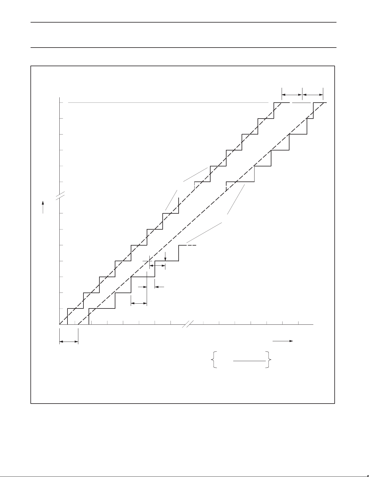
Philips Semiconductors Preliminary specification
80C51 8-bit microcontroller
16K/512 OTP/ROM/ROMless, 8 channel 10 bit A/D, I2C, PWM,
80C554/83C554/87C554
capture/compare, high I/O
Code
Out
1023
1022
1021
1020
1019
1018
Offset
error
OS
(2)
7
6
5
(5)
4
(4)
3
(1)
Gain
error
G
e
e
2
1
0
1 2 3 4 5 6 7 1018 1019 1020 1021 1022 1023 1024
Offset
error
OS
e
(1) Example of an actual transfer curve.
(2) The ideal transfer curve.
(3) Differential non-linearity (DL
(4) Integral non-linearity (IL
(5) Center of a step of the actual transfer curve.
).
e
).
e
(3)
1 LSB
(ideal)
1 LSB =
Figure 48. ADC Conversion Characteristic
AV
REF+
AVIN (LSB
– AV
1024
ideal
REF–
)
SU00212
1999 Apr 07
65
Page 66
Philips Semiconductors Preliminary specification
80C51 8-bit microcontroller
16K/512 OTP/ROM/ROMless, 8 channel 10 bit A/D, I2C, PWM,
80C554/83C554/87C554
capture/compare, high I/O
AC ELECTRICAL CHARACTERISTICS
16MHz CLOCK VARIABLE CLOCK
SYMBOL FIGURE PARAMETER MIN MAX MIN MAX UNIT
1/t
t
LHLL
t
AVLL
t
LLAX
t
LLIV
t
LLPL
t
PLPH
t
PLIV
t
PXIX
t
PXIZ
t
AVIV
t
PLAZ
CLCL
5
49 Oscillator frequency
49 ALE pulse width 85 2t
49 Address valid to ALE low 22 t
49 Address hold after ALE low 32 t
49 ALE low to valid instruction in 150 4t
49 ALE low to PSEN low 32 t
49 PSEN pulse width 142 3t
49 PSEN low to valid instruction in 82 3t
49 Input instruction hold after PSEN 0 0 ns
49 Input instruction float after PSEN 37 t
49 Address to valid instruction in 207 5t
49 PSEN low to address float 10 10 ns
Data Memory
t
RLRH
t
WLWH
t
RLDV
t
RHDX
t
RHDZ
t
LLDV
t
AVDV
t
LLWL
t
AVWL
t
QVWX
t
WHQX
t
QVWH
t
RLAZ
t
WHLH
50, 51 RD pulse width 275 6t
50, 51 WR pulse width 275 6t
50, 51 RD low to valid data in 147 5t
50, 51 Data hold after RD 0 0 ns
50, 51 Data float after RD 65 2t
50, 51 ALE low to valid data in 350 8t
50, 51 Address to valid data in 397 9t
50, 51 ALE low to RD or WR low 137 239 3t
50, 51 Address valid to WR low or RD low 122 4t
50, 51 Data valid to WR transition 13 t
50, 51 Data hold after WR 13 t
51 Data valid to WR high 287 7t
50, 51 RD low to address float 0 0 ns
50, 51 RD or WR high to ALE high 23 103 t
External Clock
t
CHCX
t
CLCX
t
CLCH
t
CHCL
52 High time 20 20 t
52 Low time 20 20 t
52 Rise time 20 20 ns
52 Fall time 20 20 ns
Shift Register
t
XLXL
t
QVXH
t
XHQX
t
XHDX
t
XHDV
53 Serial port clock cycle time 750 12t
53 Output data setup to clock rising edge 492 10t
53 Output data hold after clock rising edge 8 2t
53 Input data hold after clock rising edge 0 0 ns
53 Clock rising edge to input data valid 492 10t
NOTES:
1. Parameters are valid over operating temperature range unless otherwise specified.
2. Load capacitance for port 0, ALE, and PSEN
3. Interfacing the microcontroller to devices with float times up to 45ns is permitted. This limited bus contention will not cause damage to Port 0
drivers.
4. See application note AN457 for external memory interface.
5. Parts are guaranteed to operate down to 0Hz.
5
Speed versions : 4; 5;S 3.5 16 MHz
–40 ns
CLCL
–40 ns
CLCL
–30 ns
CLCL
–100 ns
CLCL
–30 ns
CLCL
–45 ns
CLCL
–105 ns
CLCL
–25 ns
CLCL
–105 ns
CLCL
–100 ns
CLCL
–100 ns
CLCL
–165 ns
CLCL
–60 ns
CLCL
–150 ns
CLCL
–165 ns
CLCL
–50 3t
CLCL
–130 ns
CLCL
–50 ns
CLCL
–50 ns
CLCL
–150 ns
CLCL
–40 t
CLCL
CLCL
–133 ns
CLCL
–117 ns
CLCL
+50 ns
CLCL
+40 ns
CLCL
CLCL–tCLCX
CLCL–tCHCX
–133 ns
CLCL
ns
ns
ns
= 100pF, load capacitance for all other outputs = 80pF.
1999 Apr 07
66
Page 67

Philips Semiconductors Preliminary specification
80C51 8-bit microcontroller
16K/512 OTP/ROM/ROMless, 8 channel 10 bit A/D, I2C, PWM,
80C554/83C554/87C554
capture/compare, high I/O
AC ELECTRICAL CHARACTERISTICS (Continued)
SYMBOL PARAMETER INPUT OUTPUT
I2C Interface (Refer to Figure 56)
t
HD;STA
t
LOW
t
HIGH
t
RC
t
FC
t
SU;DAT1
t
SU;DAT2
t
SU;DAT3
t
HD;DAT
t
SU;STA
t
SU;STO
t
BUF
t
RD
t
FD
STAR T condition hold time ≥ 14 t
SCL low time ≥ 16 t
SCL high time ≥ 14 t
SCL rise time ≤ 1µs –
SCL fall time ≤ 0.3µs < 0.3µs
Data set-up time ≥ 250ns > 20 t
SDA set-up time (before rep. STAR T cond.) ≥ 250ns > 1µs
SDA set-up time (before STOP cond.) ≥ 250ns > 8 t
Data hold time ≥ 0ns > 8 t
Repeated START set-up time ≥ 14 t
STOP condition set-up time ≥ 14 t
Bus free time ≥ 14 t
SDA rise time ≤ 1µs –
SDA fall time ≤ 0.3µs < 0.3µs
5
CLCL
CLCL
CLCL
CLCL
CLCL
CLCL
NOTES:
1. At 100 kbit/s. At other bit rates this value is inversely proportional to the bit-rate of 100 kbit/s.
2. Determined by the external bus-line capacitance and the external bus-line pull-resistor, this must be < 1µs.
3. Spikes on the SDA and SCL lines with a duration of less than 3 t
SCL = 400pF.
4. t
= 1/f
CLCL
interface meets the I
= one oscillator clock period at pin XTAL1. For 62ns (42s) < t
OSC
2
C-bus specification for bit-rates up to 100 kbit/s.
will be filtered out. Maximum capacitance on bus-lines SDA and
CLCL
< 285ns (16MHz (24Hz) > f
CLCL
5. These values are guaranteed but not 100% production tested.
> 4.0µs
> 4.7µs
> 4.0µs
CLCL
CLCL
CLCL
> 4.7µs
> 4.0µs
> 4.7µs
> 3.5MHz) the SI01
OSC
1
1
1
2
3
– t
RD
1
– t
FC
1
1
1
2
3
1999 Apr 07
67
Page 68
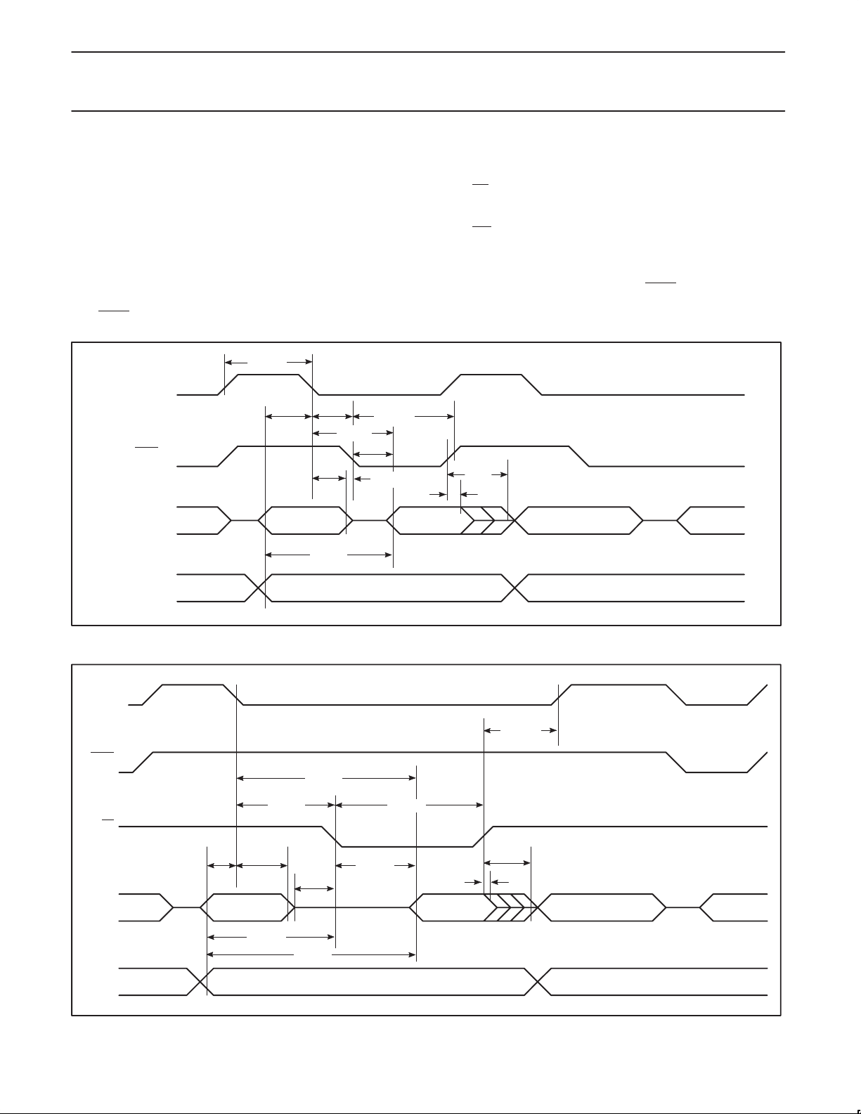
Philips Semiconductors Preliminary specification
80C51 8-bit microcontroller
16K/512 OTP/ROM/ROMless, 8 channel 10 bit A/D, I2C, PWM,
80C554/83C554/87C554
capture/compare, high I/O
EXPLANATION OF THE AC SYMBOLS
Each timing symbol has five characters. The first character is always
‘t’ (= time). The other characters, depending on their positions,
indicate the name of a signal or the logical status of that signal. The
designations are:
A – Address
C – Clock
D – Input data
H – Logic level high
I – Instruction (program memory contents)
L – Logic level low, or ALE
P – PSEN
t
ALE
LHLL
Q – Output data
R–RD
signal
t – Time
V – Valid
W– WR
signal
X – No longer a valid logic level
Z – Float
Examples: t
= Time for address valid to ALE low.
AVLL
t
= Time for ALE low to PSEN low.
LLPL
ALE
PSEN
RD
PSEN
PORT 0
PORT 2
t
t
AVLL
LLPL
t
LLAX
A0–A7 A0–A7
t
AVIV
t
PLPH
t
LLIV
t
PLIV
t
t
PLAZ
t
PXIX
INSTR IN
A0–A15 A8–A15
PXIZ
Figure 49. External Program Memory Read Cycle
t
WHLH
t
LLDV
t
LLWL
t
RLRH
SU00006
PORT 0
PORT 2
1999 Apr 07
t
AVLL
t
LLAX
A0–A7
FROM RI OR DPL
t
AVWL
t
t
t
RLAZ
t
AVDV
P2.0–P2.7 OR A8–A15 FROM DPH A0–A15 FROM PCH
RLDV
t
RHDX
DATA IN A0–A7 FROM PCL INSTR IN
RHDZ
Figure 50. External Data Memory Read Cycle
68
SU00007
Page 69
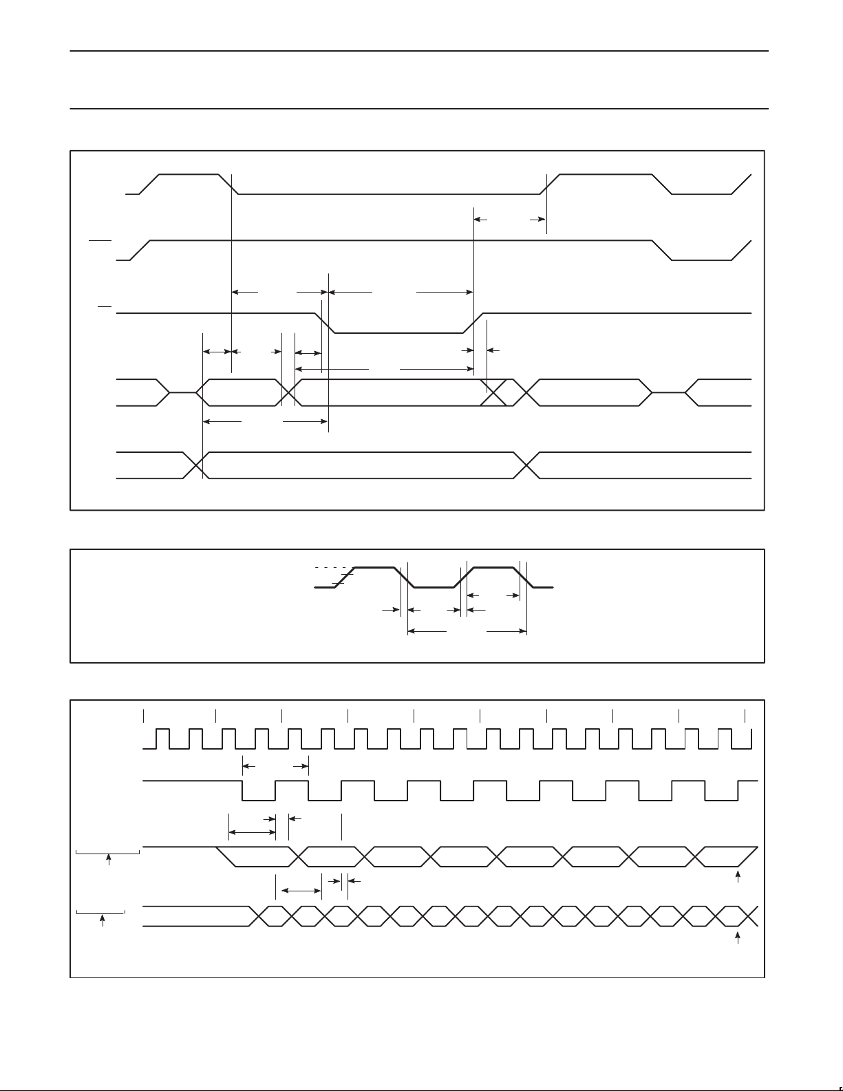
Philips Semiconductors Preliminary specification
80C51 8-bit microcontroller
16K/512 OTP/ROM/ROMless, 8 channel 10 bit A/D, I2C, PWM,
80C554/83C554/87C554
capture/compare, high I/O
ALE
t
WHLH
PSEN
WR
PORT 0
PORT 2
t
AVLL
t
t
LLAX
A0–A7
FROM RI OR DPL
t
AVWL
t
LLWL
t
QVWX
P2.0–P2.7 OR A8–A15 FROM DPH A8–A15 FROM PCH
WLWH
t
WHQX
t
DW
DATA OUT A0–A7 FROM PCL INSTR IN
Figure 51. External Data Memory Write Cycle
VCC–0.5
0.45V
0.7V
CC
0.2VCC–0.1
t
CHCL
t
CLCX
t
CLCL
t
CHCX
t
CLCH
SU00009
Figure 52. External Clock Drive XTAL1
SU00213
INSTRUCTION
ALE
CLOCK
OUTPUT DATA
WRITE TO SBUF
INPUT DATA
CLEAR RI
1999 Apr 07
012345678
t
XLXL
t
t
QVXH
t
XHDV
VALID VALID VALID VALID VALID VALID VALID VALID
XHQX
1230 4567
t
XHDX
SET TI
SET RI
SU00027
Figure 53. Shift Register Mode Timing
69
Page 70
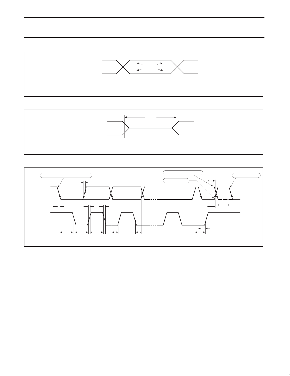
Philips Semiconductors Preliminary specification
80C51 8-bit microcontroller
16K/512 OTP/ROM/ROMless, 8 channel 10 bit A/D, I2C, PWM,
80C554/83C554/87C554
capture/compare, high I/O
START or repeated START condition
SDA
(INPUT/OUTPUT)
SCL
(INPUT/OUTPUT)
2.4V
0.45V
NOTE:
AC inputs during testing are driven at 2.4V for a logic ‘1’ and 0.45V for a logic ‘0’.
Timing measurements are made at 2.0V for a logic ‘1’ and 0.8V for a logic ‘0’.
2.0V
0.8V
Test Points
2.0V
0.8V
SU00215
Figure 54. AC Testing Input/Output
2.4V
0.45V 0.45V
NOTE:
The float state is defined as the point at which a port 0 pin sinks 3.2mA or sources 400µA at the voltage test levels.
2.0V
0.8V
Float
2.0V
0.8V
Figure 55. AC Testing Input, Float Waveform
repeated START condition
STOP condition
t
FDtRC
t
HD;STA
t
LOW
t
RD
t
HIGH
t
FC
t
SU;DAT1
t
HD;DAT
2.4V
t
SU;DAT2
SU00216
t
SU;STA
t
SU;STO
0.7 V
0.3 V
t
SU;DAT3
CC
CC
t
BUF
START condition
0.7 V
CC
0.3 V
CC
SU00107A
1999 Apr 07
Figure 56. Timing SIO1 (I2C) Interface
70
Page 71
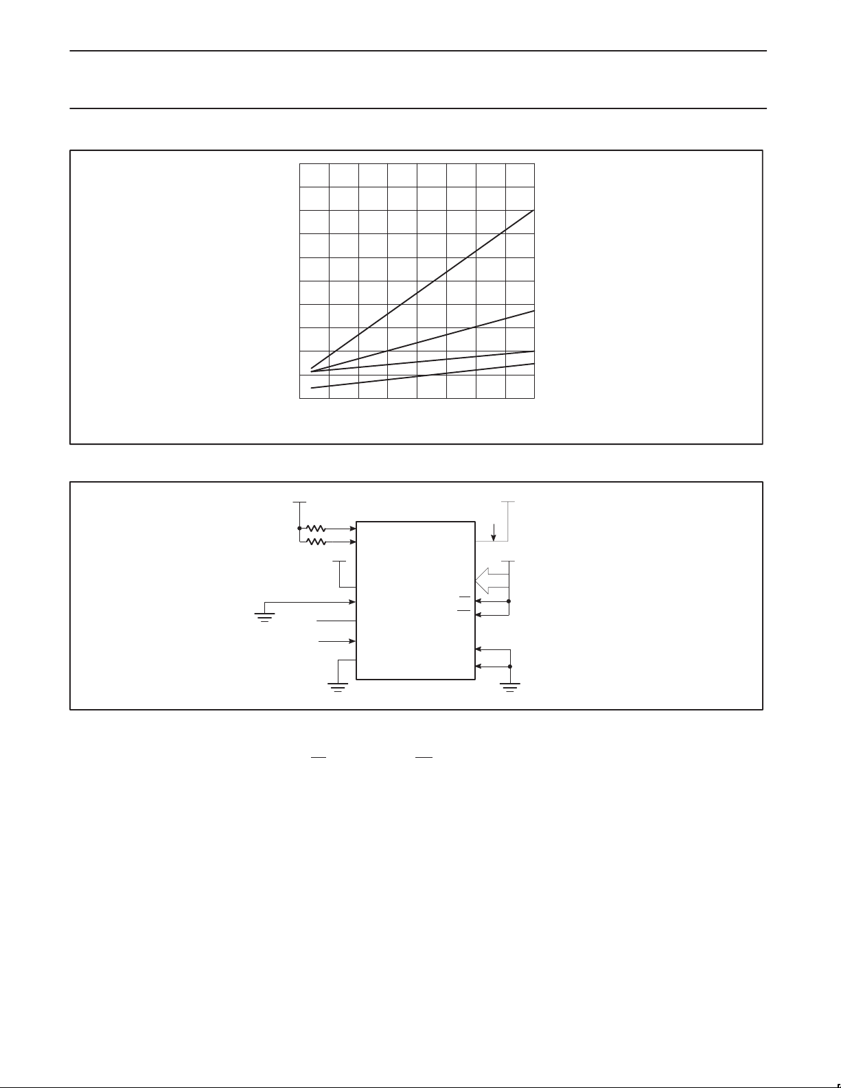
Philips Semiconductors Preliminary specification
80C51 8-bit microcontroller
16K/512 OTP/ROM/ROMless, 8 channel 10 bit A/D, I2C, PWM,
80C554/83C554/87C554
capture/compare, high I/O
20
IDD mA
16
12
8
4
0
0
f (MHz)
124168
MAXIMUM ACTIVE MODE
TYPICAL ACTIVE MODE
MAXIMUM IDLE MODE
TYPICAL IDLE MODE
SU01116
Figure 57. 16MHz Version Supply Current (IDD) as a Function of Frequency at XTAL1 (f
V
DD
(NC)
CLOCK SIGNAL
P1.6
P1.7
V
DD
RST
STADC
XTAL2
XTAL1
V
SS
V
DD
P0
EA
EW
AV
SS
AV
ref–
V
DD
I
DD
V
DD
OSC
)
Figure 58. IDD Test Condition, Active Mode
All other pins are disconnected
1. Active Mode:
a. The following pins must be forced to V
b. The following pins must be forced to V
c. Ports 1.6 and 1.7 should be connected to V
cannot exceed the I
spec of these pins.
OL1
: EA, RST, Port 0, and EW.
DD
: STADC, AVss, and AV
SS
through resistors of sufficiently high value such that the sink current into these pins
DD
ref–
.
d. The following pins must be disconnected: XTAL2 and all pins not specified above.
1999 Apr 07
71
SU00218
1
Page 72
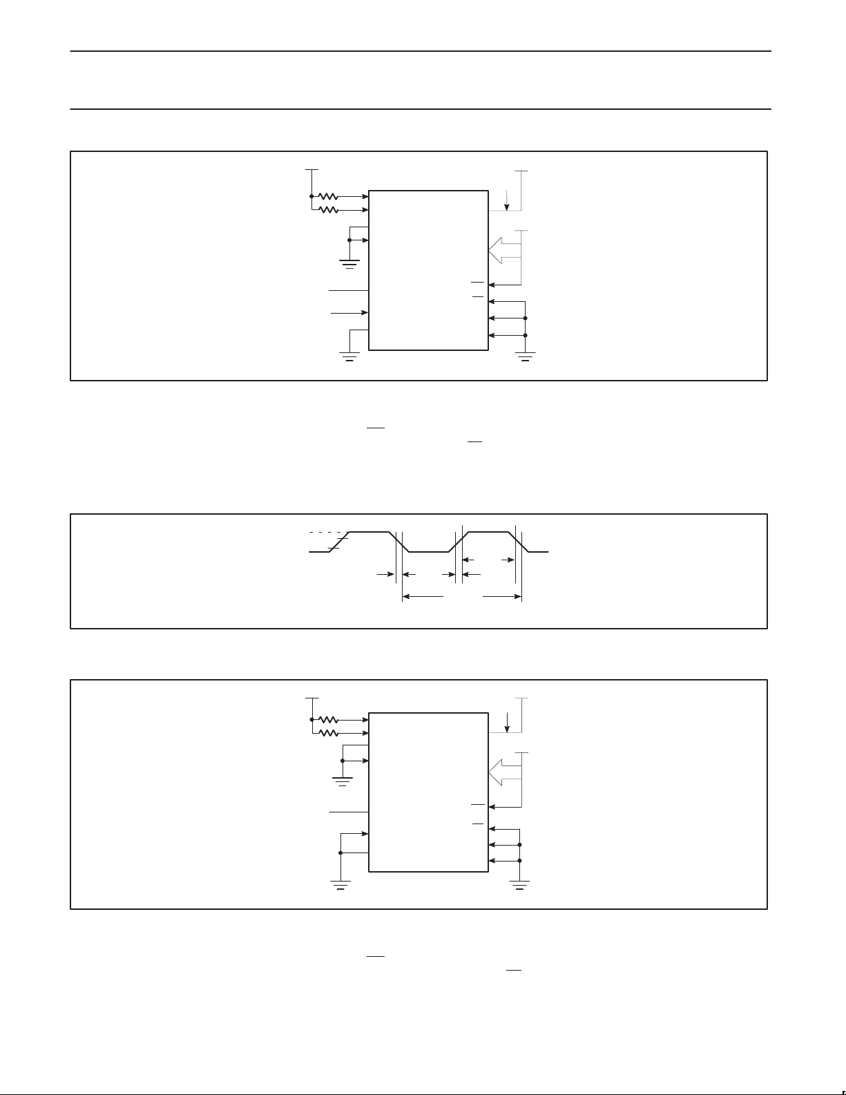
Philips Semiconductors Preliminary specification
80C51 8-bit microcontroller
16K/512 OTP/ROM/ROMless, 8 channel 10 bit A/D, I2C, PWM,
80C554/83C554/87C554
capture/compare, high I/O
V
DD
P1.6
P1.7
RST
STADC
(NC)
CLOCK SIGNAL
XTAL2
XTAL1
V
SS
AV
Figure 59. IDD Test Condition, Idle Mode
All other pins are disconnected
2. Idle Mode:
a. The following pins must be forced to V
b. The following pins must be forced to V
c. Ports 1.6 and 1.7 should be connected to V
cannot exceed the I
spec of these pins. These pins must not have logic 0 written to them prior to this measurement.
OL1
: Port 0 and EW.
DD
: RST, STADC, AVss, AV
SS
through resistors of sufficiently high value such that the sink current into these pins
DD
, and EA.
ref–
d. The following pins must be disconnected: XTAL2 and all pins not specified above.
VDD–0.5
0.5V
0.7V
DD
0.2VDD–0.1
t
CHCL
t
CLCX
t
CLCL
Figure 60. Clock Signal Waveform for IDD Tests in Active and Idle Modes
= t
t
CLCH
CHCL
= 5ns
V
DD
I
DD
V
DD
EW
AV
ref–
P0
EA
SS
t
CHCX
t
CLCH
2
V
DD
SU00219
SU00220
V
DD
P1.6
P1.7
RST
STADC
(NC)
XTAL2
XTAL1
V
SS
AV
Figure 61. IDD Test Condition, Power Down Mode
All other pins are disconnected. V
3. Power Down Mode:
a. The following pins must be forced to V
b. The following pins must be forced to V
c. Ports 1.6 and 1.7 should be connected to V
cannot exceed the I
spec of these pins. These pins must not have logic 0 written to them prior to this measurement.
OL1
: Port 0 and EW.
DD
: RST, STADC, XTAL1, AVss, AV
SS
through resistors of sufficiently high value such that the sink current into these pins
DD
d. The following pins must be disconnected: XTAL2 and all pins not specified above.
1999 Apr 07
72
V
DD
P0
EW
EA
AV
SS
ref–
= 2V to 5.5V
DD
, and EA.
ref–
V
DD
I
DD
V
DD
SU00221
3
Page 73

Philips Semiconductors Preliminary specification
80C51 8-bit microcontroller
16K/512 OTP/ROM/ROMless, 8 channel 10 bit A/D, I2C, PWM,
80C554/83C554/87C554
capture/compare, high I/O
EPROM CHARACTERISTICS
The 87C554 contains three signature bytes that can be read and
used by an EPROM programming system to identify the device. The
signature bytes identify the device as an 87C554 manufactured by
Philips:
(030H) = 15H indicates manufactured by Philips Components
(031H) = 93H indicates 87C554
(60H) = 01H
Program V erification
If security bits 2 or 3 have not been programmed, the on-chip
program memory can be read out for program verification.
If the encryption table has been programmed, the data presented at
port 0 will be the exclusive NOR of the program byte with one of the
encryption bytes. The user will have to know the encryption table
contents in order to correctly decode the verification data. The
encryption table itself cannot be read out.
Security Bits
With none of the security bits programmed the code in the program
memory can be verified. If the encryption table is programmed, the
code will be encrypted when verified. When only security bit 1 (see
Table 11) is programmed, MOVC instructions executed from external
program memory are disabled from fetching code bytes from the
internal memory, EA
of the EPROM is disabled. When security bits 1 and 2 are
programmed, in addition to the above, verify mode is disabled.
When all three security bits are programmed, all of the conditions
above apply and all external program memory execution is disabled.
is latched on Reset and all further programming
Table 11. Program Security Bits for EPROM Devices
PROGRAM LOCK BITS
SB1 SB2 SB3 PROTECTION DESCRIPTION
1 U U U No Program Security features enabled. (Code verify will still be encrypted by the Encryption Array if
2 P U U MOVC instructions executed from external program memory are disabled from fetching code bytes from
3 P P U Same as 2, also verify is disabled.
4 P P P Same as 3, external execution is disabled.
NOTES:
1. P – programmed. U – unprogrammed.
2. Any other combination of the security bits is not defined.
1, 2
programmed.)
internal memory, EA is sampled and latched on Reset, and further programming of the EPROM is disabled.
1999 Apr 07
73
Page 74
Philips Semiconductors Preliminary specification
80C51 8-bit microcontroller
16K/512 OTP/ROM/ROMless, 8 channel 10 bit A/D, I2C, PWM,
80C554/83C554/87C554
capture/compare, high I/O
ROM CODE SUBMISSION FOR 16K ROM DEVICES
When submitting ROM code for the 16k ROM devices, the following must be specified:
1. 16k byte user ROM data
2. 64 byte ROM encryption key
3. ROM security bits.
ADDRESS
0000H to 3FFFH DATA 7:0 User ROM Data
4000H to 403FH KEY 7:0 ROM Encryption Key
4040H SEC 0 ROM Security Bit 1
4040H SEC 1 ROM Security Bit 2
4040H SEC 2 ROM Security Bit 3
Security Bit 1: When programmed, this bit has two effects on masked ROM parts:
1. External MOVC is disabled, and
is latched on Reset.
2. EA
Security Bit 2: When programmed, this bit inhibits Verify User ROM.
NOTE: Security Bit 2 cannot be enabled unless Security Bit 1 is enabled.
Security Bit 3: When programmed, inhibits external execution.
If the ROM Code file does not include the options, the following information must be included with the ROM code.
For each of the following, check the appropriate box, and send to Philips along with the code:
Security Bit #1:
V Enabled V Disabled
CONTENT BIT(S) COMMENT
FFH = no encryption
0 = enable security
1 = disable security
0 = enable security
1 = disable security
0 = enable security
1 = disable security
Security Bit #2: V Enabled V Disabled
Security Bit #3:
Encryption:
V Enabled V Disabled
V No V Yes If Yes, must send key file.
Purchase of Philips I2C components conveys a license under the Philips’ I2C patent
to use the components in the I2C system provided the system conforms to the
I2C specifications defined by Philips. This specification can be ordered using the
code 9398 393 40011.
1999 Apr 07
74
Page 75
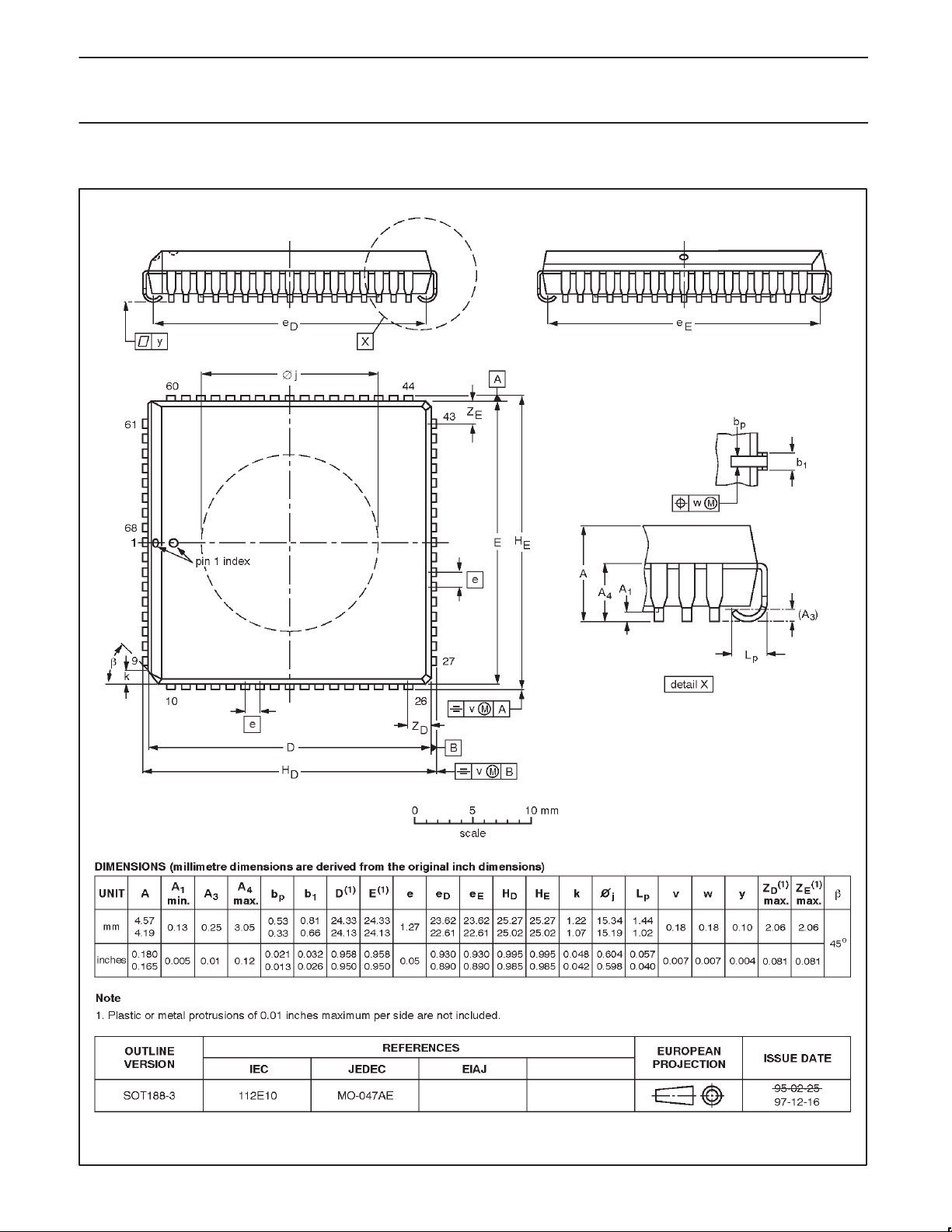
Philips Semiconductors Preliminary specification
80C51 8-bit microcontroller
16K/512 OTP/ROM/ROMless, 8 channel 10 bit A/D, I2C, PWM,
80C554/83C554/87C554
capture/compare, high I/O
PLCC68: plastic leaded chip carrier; 68 leads; pedestal SOT188-3
1999 Apr 07
75
Page 76
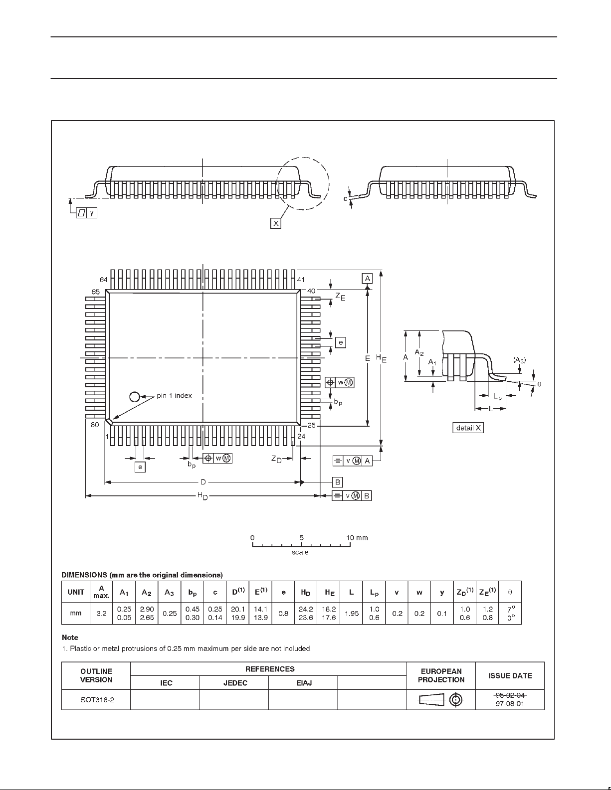
Philips Semiconductors Preliminary specification
80C51 8-bit microcontroller
16K/512 OTP/ROM/ROMless, 8 channel 10 bit A/D, I2C, PWM,
80C554/83C554/87C554
capture/compare, high I/O
QFP80: plastic quad flat package; 80 leads (lead length 1.95 mm); body 14 x 20 x 2.8 mm SOT318-2
1999 Apr 07
76
Page 77

Philips Semiconductors Preliminary specification
80C51 8-bit microcontroller
16K/512 OTP/ROM/ROMless, 8 channel 10 bit A/D, I2C, PWM,
capture/compare, high I/O
NOTES
80C554/83C554/87C554
1999 Apr 07
77
Page 78

Philips Semiconductors Preliminary specification
80C51 8-bit microcontroller
16K/512 OTP/ROM/ROMless, 8 channel 10 bit A/D, I2C, PWM,
capture/compare, high I/O
Data sheet status
Data sheet
status
Objective
specification
Preliminary
specification
Product
specification
Product
status
Development
Qualification
Production
Definition
This data sheet contains the design target or goal specifications for product development.
Specification may change in any manner without notice.
This data sheet contains preliminary data, and supplementary data will be published at a later date.
Philips Semiconductors reserves the right to make chages at any time without notice in order to
improve design and supply the best possible product.
This data sheet contains final specifications. Philips Semiconductors reserves the right to make
changes at any time without notice in order to improve design and supply the best possible product.
[1]
80C554/83C554/87C554
[1] Please consult the most recently issued datasheet before initiating or completing a design.
Definitions
Short-form specification — The data in a short-form specification is extracted from a full data sheet with the same type number and title. For
detailed information see the relevant data sheet or data handbook.
Limiting values definition — Limiting values given are in accordance with the Absolute Maximum Rating System (IEC 134). Stress above one
or more of the limiting values may cause permanent damage to the device. These are stress ratings only and operation of the device at these or
at any other conditions above those given in the Characteristics sections of the specification is not implied. Exposure to limiting values for extended
periods may affect device reliability.
Application information — Applications that are described herein for any of these products are for illustrative purposes only. Philips
Semiconductors make no representation or warranty that such applications will be suitable for the specified use without further testing or
modification.
Disclaimers
Life support — These products are not designed for use in life support appliances, devices or systems where malfunction of these products can
reasonably be expected to result in personal injury . Philips Semiconductors customers using or selling these products for use in such applications
do so at their own risk and agree to fully indemnify Philips Semiconductors for any damages resulting from such application.
Right to make changes — Philips Semiconductors reserves the right to make changes, without notice, in the products, including circuits, standard
cells, and/or software, described or contained herein in order to improve design and/or performance. Philips Semiconductors assumes no
responsibility or liability for the use of any of these products, conveys no license or title under any patent, copyright, or mask work right to these
products, and makes no representations or warranties that these products are free from patent, copyright, or mask work right infringement, unless
otherwise specified.
Philips Semiconductors
811 East Arques Avenue
P.O. Box 3409
Sunnyvale, California 94088–3409
Telephone 800-234-7381
Copyright Philips Electronics North America Corporation 1999
All rights reserved. Printed in U.S.A.
Date of release: 04-99
Document order number: 9397 750 05503
1999 Apr 07
78
 Loading...