

Page 1
INTEGRATED CIRCUITS
89C535/89C536/89C538
CMOS single-chip 8-bit microcontrollers
with FLASH program memory
Preliminary specification
IC20 Data Handbook
1997 June 05
Page 2
Philips Semiconductors Preliminary specification
CMOS single-chip 8-bit microcontrollers
with FLASH program memory
DESCRIPTION
The 89C535/89C536/89C538 are Single-Chip 8-Bit Microcontrollers
manufactured in advanced CMOS process and are derivatives of
the 80C51 microcontroller family. All the devices have the same
instruction set as the 80C51.
The devices also have four 8-bit I/O ports, three 16-bit timer/event
counters, a multi-source, two-priority-level, nested interrupt
structure, UART and on-chip oscillator and timing circuits. For
systems that require extra data memory capability up to 64k bytes,
each can be expanded using standard TTL-compatible memories
and logic.
The 89C535/89C536/89C538 contain a non-volatile FLASH EPROM
program memory (8K bytes in 89C535, 16k bytes in the 89C536,
and 64k bytes in the 89C538). The devices have 512 bytes of RAM
data memory.
FEA TURES
•80C51 Central Processing Unit
•8k x 8 (89C535) 16k × 8 (89C536) or 64k × 8 (89C538), FLASH
EPROM Program Memory
•512 × 8 RAM, externally expandable to 64k × 8 Data Memory
•Three 16-bit counter/timers
•Up to 3 external interrupt request inputs
•6 interrupt sources with 2 priority levels
•Four 8-bit I/O ports
•Full-duplex UART
•Power control modes
– Idle mode
– Power down mode, with wakeup from power down using
external interrupt
•44-pin PLCC and QFP packages
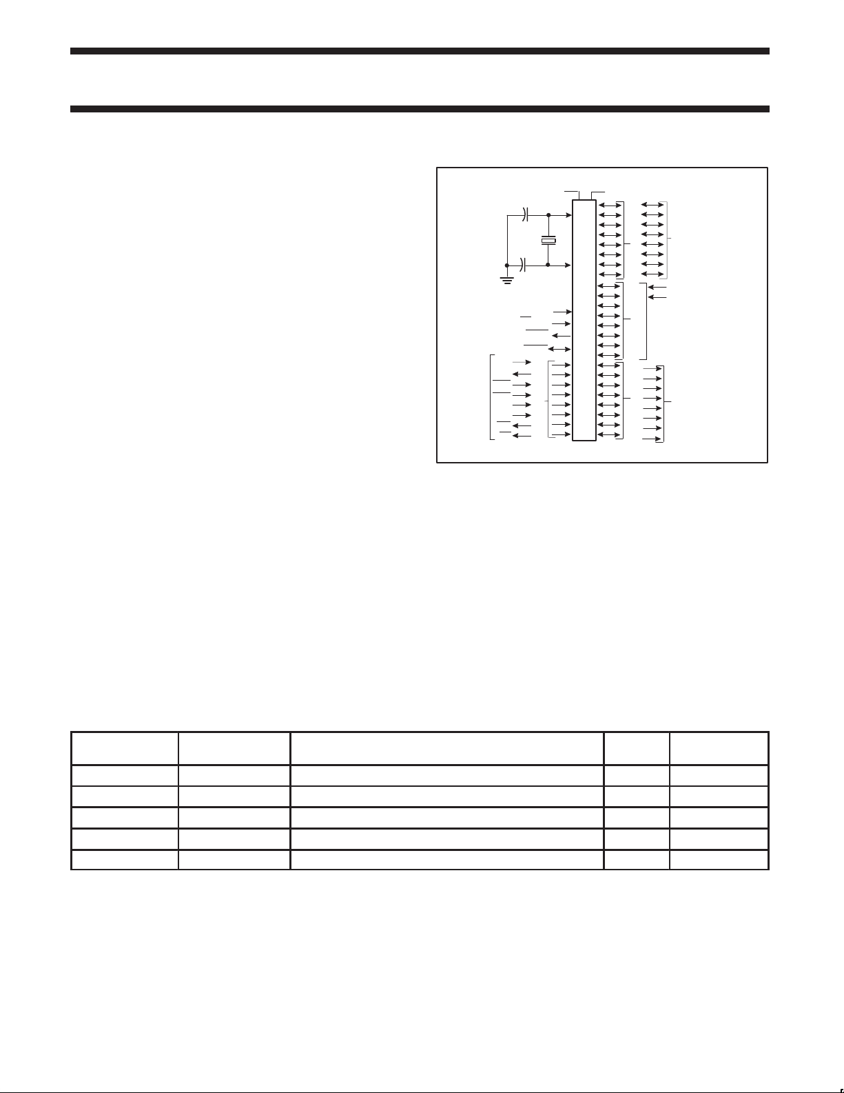
LOGIC SYMBOL
RST
EA/V
PSEN
ALE/PROG
RxD
TxD
INT0
INT1
T0
T1
WR
RD
SECONDARY FUNCTIONS
89C535/89C536/89C538
V
V
SS
CC
XTAL1
ADDRESS AND
PORT 0
XTAL2
PP
PORT 3
DATA BUS
T2
T2EX
PORT 1PORT 2
ADDRESS BUS
SU00830
ORDERING INFORMA TION
PART NUMBER MEMORY SIZE TEMPERATURE RANGE (°C) AND PACKAGE
P89C535NBA A 8k bytes 0 to +70, 44-pin Plastic Leaded Chip Carrier 33 SOT187-2
P89C536NBA A 16k bytes 0 to +70, 44-pin Plastic Leaded Chip Carrier 33 SOT187-2
P89C536NBB B 16k bytes 0 to +70, 44-pin Plastic Quad Flat Package 33 SOT307-2
P89C538NBA A 64k bytes 0 to +70, 44-pin Plastic Leaded Chip Carrier 33 SOT187-2
P89C538NBB B 64k bytes 0 to +70, 44-pin Plastic Quad Flat Package 33 SOT307-2
1997 Jun 05
2
FREQ.
(MHz)
DRAWING
NUMBER
Page 3
Philips Semiconductors Preliminary specification
CMOS single-chip 8-bit microcontrollers
with FLASH program memory
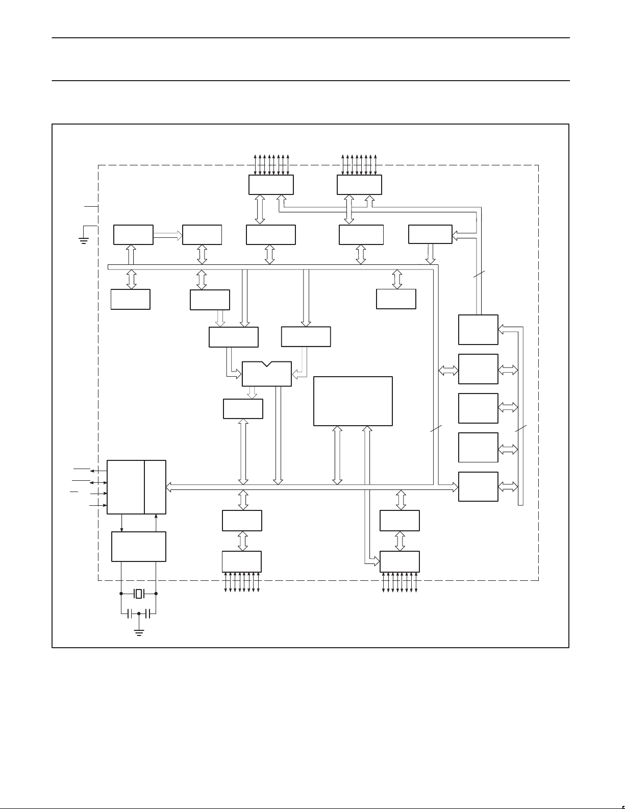
BLOCK DIAGRAM
P0.0–P0.7 P2.0–P2.7
PORT 0
DRIVERS
V
CC
V
SS
RAM ADDR
REGISTER
B
REGISTER
RAM
ACC
TMP2
PORT 0
LATCH
TMP1
PORT 2
DRIVERS
PORT 2
LATCH
89C535/89C536/89C538
ROF/EPROM
8
STACK
POINTER
PROGRAM
ADDRESS
REGISTER
PSEN
ALE/PROG
EAV
PP
RST
TIMING
AND
CONTROL
OSCILLATOR
XTAL1 XTAL2
INSTRUCTION
PD
REGISTER
PSW
PORT 1
LATCH
PORT 1
DRIVERS
P1.0–P1.7
ALU
SFRs
TIMERS
PORT 3
LATCH
PORT 3
DRIVERS
P3.0–P3.7
BUFFER
PC
INCRE-
MENTER
8 16
PROGRAM
COUNTER
DPTR’S
MULTIPLE
SU00854
1997 Jun 05
3
Page 4
Philips Semiconductors Preliminary specification
CMOS single-chip 8-bit microcontrollers
with FLASH program memory
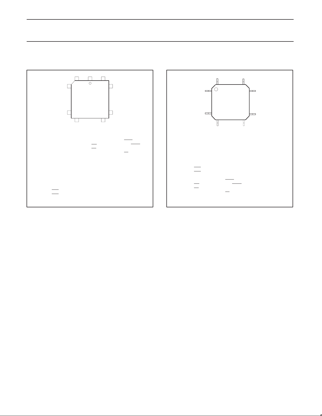
CERAMIC AND PLASTIC LEADED CHIP CARRIER PIN FUNCTIONS
6140
7
17
Pin Function
1V
SS
2 P1.0/T2
3 P1.1/T2EX
4 P1.2/ECI
5 P1.3
6 P1.4
7 P1.5
8 P1.6
9 P1.7
10 RST
11 P3.0/RxD
12 NIC*
13 P3.1/TxD
14 P3.2/INT0
15 P3.3/INT1
* NO INTERNAL CONNECTION
LCC
18 28
Pin Function
16 P3.4/T0
17 P3.5/T1
18 P3.6/WR
19 P3.7/RD
20 XTAL2
21 XTAL1
22 V
SS
23 V
CC
24 P2.0/A8
25 P2.1/A9
26 P2.2/A10
27 P2.3/A11
28 P2.4/A12
29 P2.5/A13
30 P2.6/A14
39
29
Pin Function
31 P2.7/A15
32 PSEN
33 ALE/PROG
34 NIC*
35 EA
/V
36 P0.7/AD7
37 P0.6/AD6
38 P0.5/AD5
39 P0.4/AD4
40 P0.3/AD3
41 P0.2/AD2
42 P0.1/AD1
43 P0.0/AD0
44 V
PP
CC
SU00852A
89C535/89C536/89C538
PLASTIC QUAD FLAT PACK PIN FUNCTIONS
44 34
1
PQFP
11
12 22
Pin Function
1 P1.5
2 P1.6
3 P1.7
4 RST
5 P3.0/RxD
6 NIC*
7 P3.1/TxD
8 P3.2/INT0
9 P3.3/INT1
10 P3.4/T0
11 P3.5/T1
12 P3.6/WR
13 P3.7/RD
14 XTAL2
15 XTAL1
* NO INTERNAL CONNECTION
Pin Function
16 V
SS
17 V
CC
18 P2.0/A8
19 P2.1/A9
20 P2.2/A10
21 P2.3/A11
22 P2.4/A12
23 P2.5/A13
24 P2.6/A14
25 P2.7/A15
26 PSEN
27 ALE/PROG
28 NIC*
29 EA
/V
30 P0.7/AD7
33
23
Pin Function
31 P0.6/AD6
32 P0.5/AD5
33 P0.4/AD4
34 P0.3/AD3
35 P0.2/AD2
36 P0.1/AD1
37 P0.0/AD0
38 V
CC
39 V
SS
40 P1.0/T2
41 P1.1/T2EX
42 P1.2
43 P1.3
PP
44 P1.4
SU00853A
1997 Jun 05
4
Page 5
Philips Semiconductors Preliminary specification
CMOS single-chip 8-bit microcontrollers
with FLASH program memory
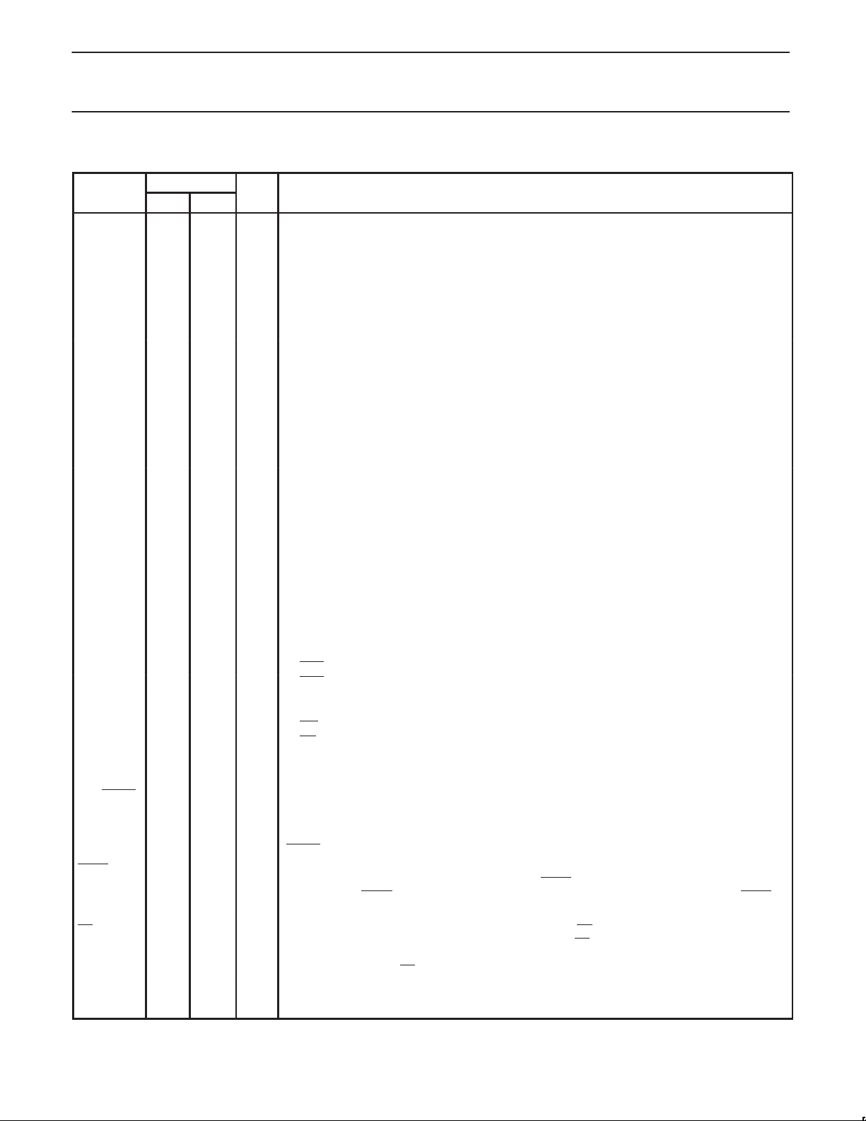
PIN DESCRIPTIONS
PIN NUMBER
MNEMONIC LCC QFP TYPE NAME AND FUNCTION
V
SS
V
CC
P0.0–0.7 43–36 37–30 I/O Port 0: Port 0 is an open-drain, bidirectional I/O port. Port 0 pins that have 1s written to them float
P1.0–P1.7 2–9 40–44,
P2.0–P2.7 24–31 18–25 I/O Port 2: Port 2 is an 8-bit bidirectional I/O port with internal pull-ups. Port 2 pins that have 1s written
P3.0–P3.7 11,
RST 10 4 I Reset: A high on this pin for two machine cycles while the oscillator is running, resets the device. An
ALE/PROG 33 27 O Address Latch Enable/Program Pulse: Output pulse for latching the low byte of the address
PSEN 32 26 O Program Store Enable: The read strobe to external program memory. When the processor is
EA/V
PP
XTAL1 21 15 I Crystal 1: Input to the inverting oscillator amplifier and input to the internal clock generator circuits.
XTAL2 20 14 O Crystal 2: Output from the inverting oscillator amplifier.
NOTE:
To avoid “latch-up” effect at power-on, the voltage on any pin at any time must not be higher than V
1, 22 16, 39 I Ground: 0V reference.
23, 44 17, 38 I Power Supply: This is the power supply voltage for normal, idle, and power-down operation.
and can be used as high-impedance inputs. Port 0 is also the multiplexed low-order address and
data bus during accesses to external program and data memory. In this application, it uses strong
internal pull-ups when emitting 1s. Port 0 also outputs the code bytes during program verification and
received code bytes during EEPROM programming. External pull-ups are required during program
verification.
1–3
2 40 I/O T2 (P1.0): Timer/Counter 2 external count input
3 41 I T2EX (P1.1): Timer/Counter 2 Reload/Capture
13–195,7–13
11 5 I RxD (P3.0): Serial input port
13 7 O TxD (P3.1): Serial output port
14 8 I INT0 (P3.2): External interrupt
15 9 I INT1 (P3.3): External interrupt
16 10 I T0 (P3.4): Timer 0 external input
17 11 I T1 (P3.5): Timer 1 external input
18 12 O WR (P3.6): External data memory write strobe
19 13 O RD (P3.7): External data memory read strobe
35 29 I External Access Enable/Programming Supply Voltage: EA must be externally held low to enable
I/O Port 1: Port 1 is an 8-bit bidirectional I/O port with internal pull-ups. Port 1 pins that have 1s written
to them are pulled high by the internal pull-ups and can be used as inputs. As inputs, port 1 pins that
are externally pulled low will source current because of the internal pull-ups. (See DC Electrical
Characteristics: I
verification.
Alternate functions for Port 1 include:
to them are pulled high by the internal pull-ups and can be used as inputs. As inputs, port 2 pins that
are externally being pulled low will source current because of the internal pull-ups. (See DC
Electrical Characteristics: I
program memory and during accesses to external data memory that use 16-bit addresses (MOVX
@DPTR). In this application, it uses strong internal pull-ups when emitting 1s. Some Port 2 pins
receive the high order address bits during EEPROM programming and verification.
I/O Port 3: Port 3 is an 8-bit bidirectional I/O port with internal pull-ups. Port 3 pins that have 1s written
to them are pulled high by the internal pull-ups and can be used as inputs. As inputs, port 3 pins that
are externally being pulled low will source current because of the pull-ups. (See DC Electrical
Characteristics: I
internal diffused resistor to V
during an access to external memory. In normal operation, ALE is emitted at a constant rate of 1/6
the oscillator frequency , and can be used for external timing or clocking. Note that one ALE pulse is
skipped during each access to external data memory. This pin is also the program pulse input
) during EEPROM programming.
(PROG
executing code from the external program memory, PSEN
except that two PSEN
not activated during fetches from internal program memory.
the device to fetch code from external program memory. If EA
internal program memory. This pin also receives the 12V programming supply voltage (V
EPROM programming. EA
). Port 1 also receives the low-order address byte during program memory
IL
). Port 2 emits the high-order address byte during fetches from external
IL
). Port 3 also serves the special features of the 80C51 family, as listed below:
IL
permits a power-on reset using only an external capacitor to VCC.
SS
activations are skipped during each access to external data memory. PSEN is
is internally latched on Reset.
89C535/89C536/89C538
is activated twice each machine cycle,
is held high, the device executes from
+ 0.5V or VSS – 0.5V, respectively.
CC
) during
PP
1997 Jun 05
5
Page 6
Philips Semiconductors Preliminary specification
CMOS single-chip 8-bit microcontrollers
with FLASH program memory
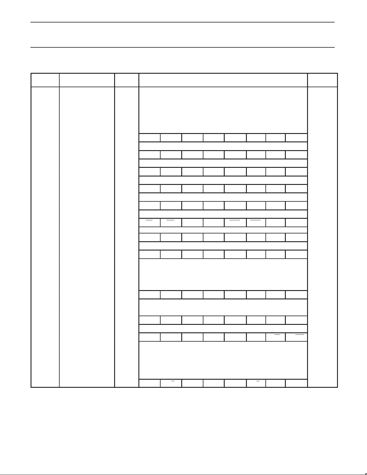
Table 1. Special Function Registers
SYMBOL DESCRIPTION
ACC* Accumulator E0H E7 E6 E5 E4 E3 E2 E1 E0 00H
B* B register F0H F7 F6 F5 F4 F3 F2 F1 F0 00H
DPTR: Data Pointer (2 bytes)
DPH Data Pointer High 83H 00H
DPL Data Pointer Low 82H 00H
IE* Interrupt Enable A8H EA – ET2 ES ET1 EX1 ET0 EX0 00H
IP* Interrupt Priority B8H – – PT2 PS PT1 PX1 PT0 PX0 x0000000B
P0* Port 0 80H AD7 AD6 AD5 AD4 AD3 AD2 AD1 AD0 FFH
P1* Port 1 90H – – – – – – T2EX T2 FFH
P2* Port 2 A0H AD15 AD14 AD13 AD12 AD11 AD10 AD9 AD8 FFH
P3* Port 3 B0H RD WR T1 T0 INT1 INT0 TxD RxD FFH
DIRECT
ADDRESS
BIT ADDRESS, SYMBOL, OR ALTERNATIVE PORT FUNCTION
MSB LSB
AF AE AD AC AB AA A9 A8
BF BE BD BC BB BA B9 B8
87 86 85 84 83 82 81 80
97 96 95 94 93 92 91 90
A7 A6 A5 A4 A3 A2 A1 A0
B7 B6 B5 B4 B3 B2 B1 B0
89C535/89C536/89C538
RESET
VALUE
PCON# Power Control 87H SMOD – – – GF1 GF0 PD IDL 0xxxx000B
D7 D6 D5 D4 D3 D2 D1 D0
PSW* Program Status Word D0H CY AC F0 RS1 RS0 OV – P 00H
RACAP2H# Timer 2 Capture High CBH 00H
RACAP2L# Timer 2 Capture Low CAH 00H
SBUF Serial Data Buffer 99H xxxxxxxxB
9F 9E 9D 9C 9B 9A 99 98
SCON* Serial Control 98H SM0 SM1 SM2 REN TB8 RB8 TI RI 00H
SP Stack Pointer 81H 07H
8F 8E 8D 8C 8B 8A 89 88
TCON* T imer Control 88H TF1 TR1 TF0 TR0 IE1 IT1 IE0 IT0 00H
CF CE CD CC CB CA C9 C8
T2CON* Timer 2 Control C8H TF2 EXF2 RCLK TCLK EXEN2 TR2 C/T2 CP/RL2 00H
TH0 Timer High 0 8CH 00H
TH1 Timer High 1 8DH 00H
TH2# Timer High 2 CDH 00H
TL0 Timer Low 0 8AH 00H
TL1 Timer Low 1 8BH 00H
TL2# Timer Low 2 CCH 00H
TMOD Timer Mode 89H GATE C/T M1 M0 GA TE C/T M1 M0 00H
* SFRs are bit addressable.
# SFRs are modified from or added to the 80C51 SFRs.
– Reserved bits.
1997 Jun 05
6
Page 7
Philips Semiconductors Preliminary specification
CMOS single-chip 8-bit microcontrollers
with FLASH program memory
OSCILLA T OR CHARACTERISTICS
XTAL1 and XTAL2 are the input and output, respectively , of an
inverting amplifier . The pins can be configured for use as an on-chip
oscillator.
To drive the device from an external clock source, XTAL1 should be
driven while XTAL2 is left unconnected. There are no requirements
on the duty cycle of the external clock signal, because the input to
the internal clock circuitry is through a divide-by-two flip-flop.
However, minimum and maximum high and low times specified in
the data sheet must be observed.
RESET
A reset is accomplished by holding the RST pin high for at least two
machine cycles (24 oscillator periods), while the oscillator is running.
To insure a good power-on reset, the RST pin must be high long
enough to allow the oscillator time to start up (normally a few
milliseconds) plus two machine cycles. At power-on, the voltage on
V
and RST must come up at the same time for a proper start-up.
CC
Ports 1, 2, and 3 will asynchronously be driven to their reset
condition when a voltage above V
LOW POWER MODES
Idle Mode
In the idle mode (see Table 2), the CPU puts itself to sleep while all
of the on-chip peripherals stay active. The instruction to invoke the
idle mode is the last instruction executed in the normal operating
mode before the idle mode is activated. The CPU contents, the
on-chip RAM, and all of the special function registers remain intact
during this mode. The idle mode can be terminated either by any
enabled interrupt (at which time the process is picked up at the
interrupt service routine and continued), or by a hardware reset
which starts the processor in the same manner as a power-on reset.
Power-Down Mode
To save even more power, a Power Down mode (see Table 2) can
be invoked by software. In this mode, the oscillator is stopped and
(min.) is applied to RESET.
IH1
89C535/89C536/89C538
the instruction that invoked Power Down is the last instruction
executed. The on-chip RAM and Special Function Registers retain
their values down to 2.0V and care must be taken to return V
the minimum specified operating voltages before the Power Down
Mode is terminated.
Either a hardware reset or external interrupt can be used to exit from
Power Down. Reset redefines all the SFRs but does not change the
on-chip RAM. An external interrupt allows both the SFRs and the
on-chip RAM to retain their values.
To properly terminate Power Down the reset or external interrupt
should not be executed before V
operating level and must be held active long enough for the
oscillator to restart and stabilize (normally less than 10ms).
With an external interrupt, INT0 and INT1 must be enabled and
configured as level-sensitive. Holding the pin low restarts the
oscillator but bringing the pin back high completes the exit. Once the
interrupt is serviced, the next instruction to be executed after RETI
will be the one following the instruction that put the device into
Power Down.
is restored to its normal
CC
Design Consideration
•To eliminate the possibility of an unexpected write when Idle is
terminated by reset, the instruction following the one that invokes
Idle should not be one that writes to a port pin or to memory.
ONCE Mode
The ONCE (“On-Circuit Emulation”) Mode facilitates testing and
debugging of systems without the device having to be removed from
the circuit. The ONCE Mode is invoked by:
1. Pull ALE low while the device is in reset and PSEN
2. Hold ALE low as RST is deactivated.
While the device is in ONCE Mode, the Port 0 pins go into a float
state, and the other port pins and ALE and PSEN
high. The oscillator circuit remains active. While the 8XC51FA/FB is
in this mode, an emulator or test CPU can be used to drive the
circuit. Normal operation is restored when a normal reset is applied.
is high;
are weakly pulled
CC
to
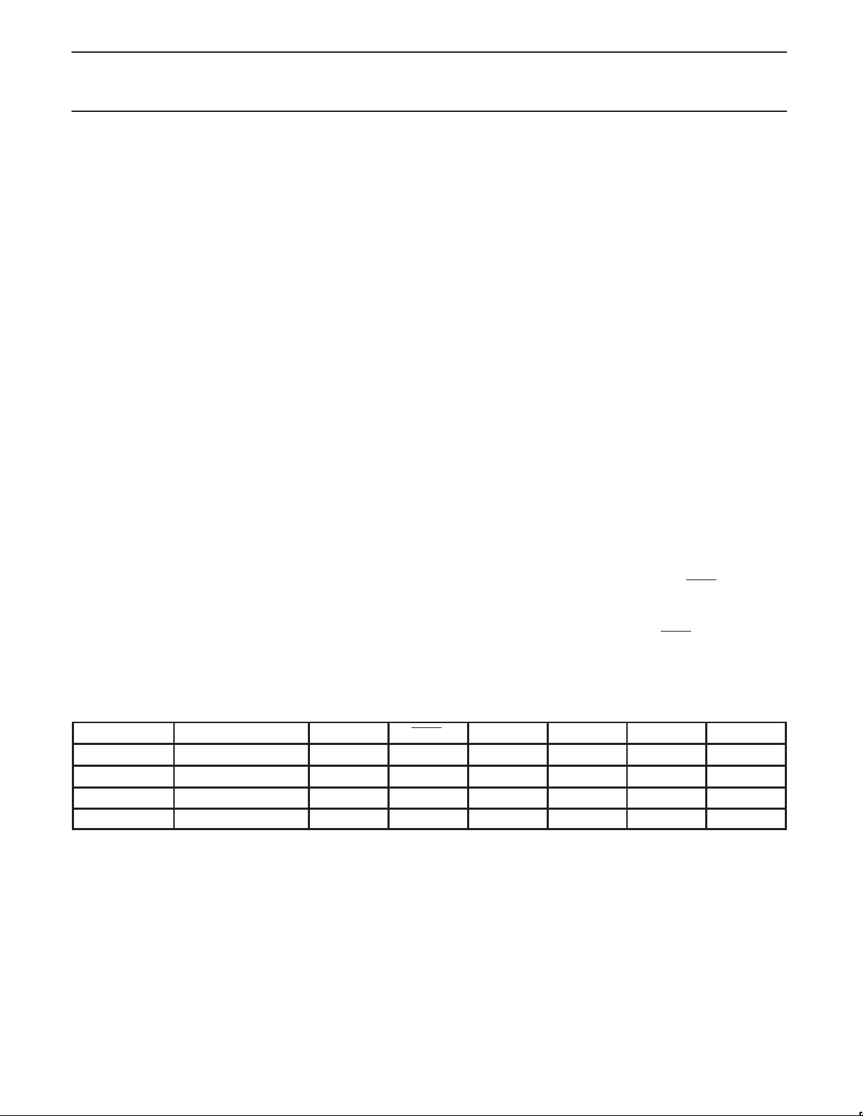
Table 2. External Pin Status During Idle and Power-Down Mode
MODE PROGRAM MEMORY ALE PSEN PORT 0 PORT 1 PORT 2 PORT 3
Idle Internal 1 1 Data Data Data Data
Idle External 1 1 Float Data Address Data
Power-down Internal 0 0 Data Data Data Data
Power-down External 0 0 Float Data Data Data
1997 Jun 05
7
Page 8
Philips Semiconductors Preliminary specification
CMOS single-chip 8-bit microcontrollers
with FLASH program memory
TIMER 2 OPERATION
Timer 2
Timer 2 is a 16-bit Timer/Counter which can operate as either an
event timer or an event counter, as selected by C/T2* in the special
function register T2CON (see Figure 1). Timer 2 has three operating
modes:Capture, Auto-reload, and Baud Rate Generator, which are
selected by bits in the T2CON as shown in Table 3.
Capture Mode
In the capture mode there are two options which are selected by bit
EXEN2 in T2CON. If EXEN2=0, then timer 2 is a 16-bit timer or
counter (as selected by C/T2* in T2CON) which, upon overflowing
sets bit TF2, the timer 2 overflow bit. This bit can be used to
generate an interrupt (by enabling the Timer 2 interrupt bit in the
IE register/SFR table). If EXEN2= 1, Timer 2 operates as described
above, but with the added feature that a 1- to -0 transition at external
input T2EX causes the current value in the Timer 2 registers, TL2
and TH2, to be captured into registers RCAP2L and RCAP2H,
respectively. In addition, the transition at T2EX causes bit EXF2 in
T2CON to be set, and EXF2 like TF2 can generate an interrupt
(which vectors to the same location as Timer 2 overflow interrupt.
The Timer 2 interrupt service routine can interrogate TF2 and EXF2
to determine which event caused the interrupt). The capture mode is
89C535/89C536/89C538
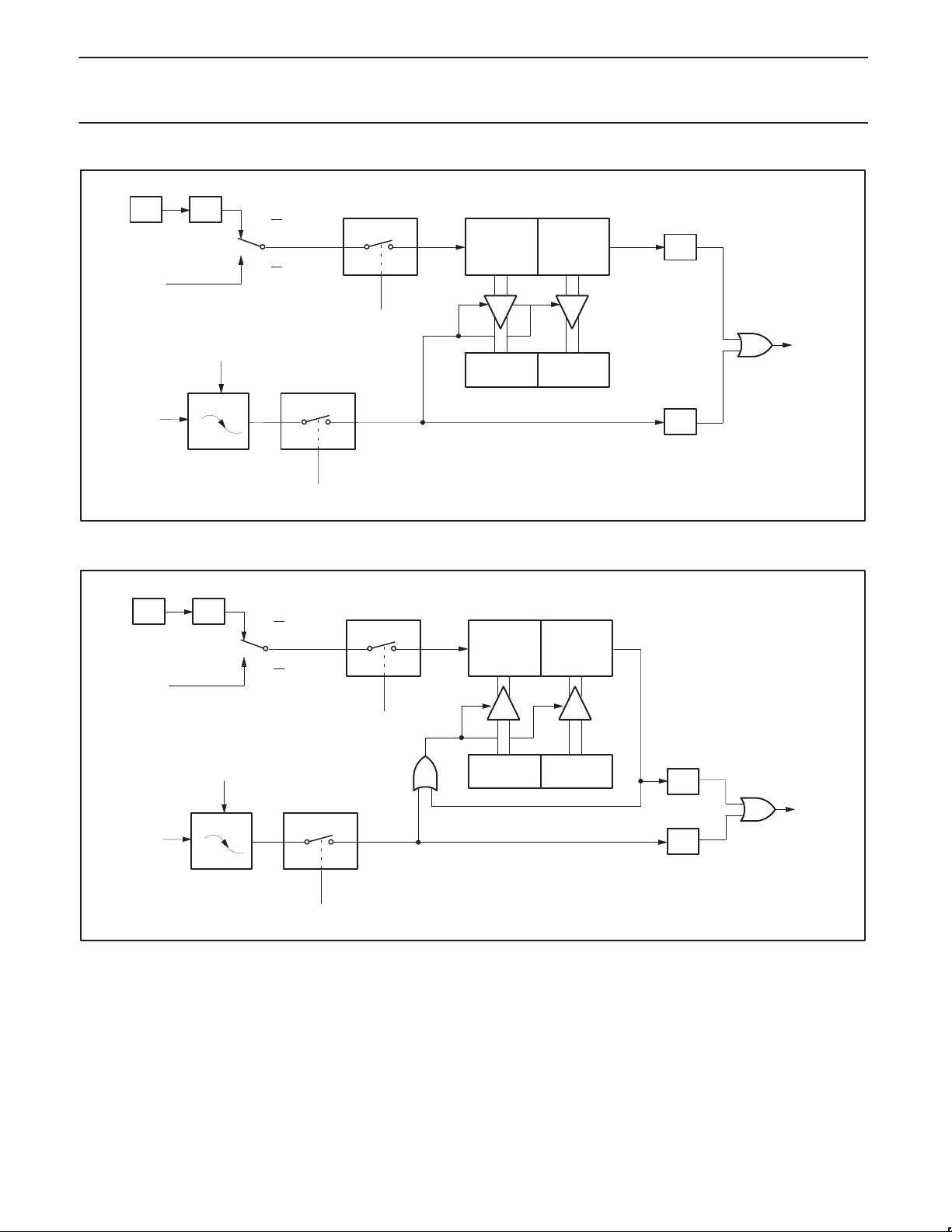
illustrated in Figure 2 (There is no reload value for TL2 and TH2 in
this mode. Even when a capture event occurs from T2EX, the
counter keeps on counting T2EX pin transitions or osc/12 pulses.).
Auto-Reload Mode
In the 16-bit auto-reload mode, Timer 2 can be configured as either
a timer or counter (C/T2* in T2CON).
Figure 3 shows the auto–reload mode of Timer 2. In this mode there
are two options selected by bit EXEN2 in T2CON register. If
EXEN2=0, then Timer 2 counts up to 0FFFFH and sets the TF2
(Overflow Flag) bit upon overflow. This causes the Timer 2 registers
to be reloaded with the 16-bit value in RCAP2L and RCAP2H.
The values in RCAP2L and RCAP2H are preset by software. If
EXEN2=1, then a 16-bit reload can be triggered either by an
overflow or by a 1-to-0 transition at input T2EX. This transition also
sets the EXF2 bit. The Timer 2 interrupt, if enabled, can be
generated when either TF2 or EXF2 are 1.
The external flag EXF2 toggles when Timer 2 underflows or
overflows. This EXF2 bit can be used as a 17th bit of resolution if
needed. The EXF2 flag does not generate an interrupt in this mode
of operation.
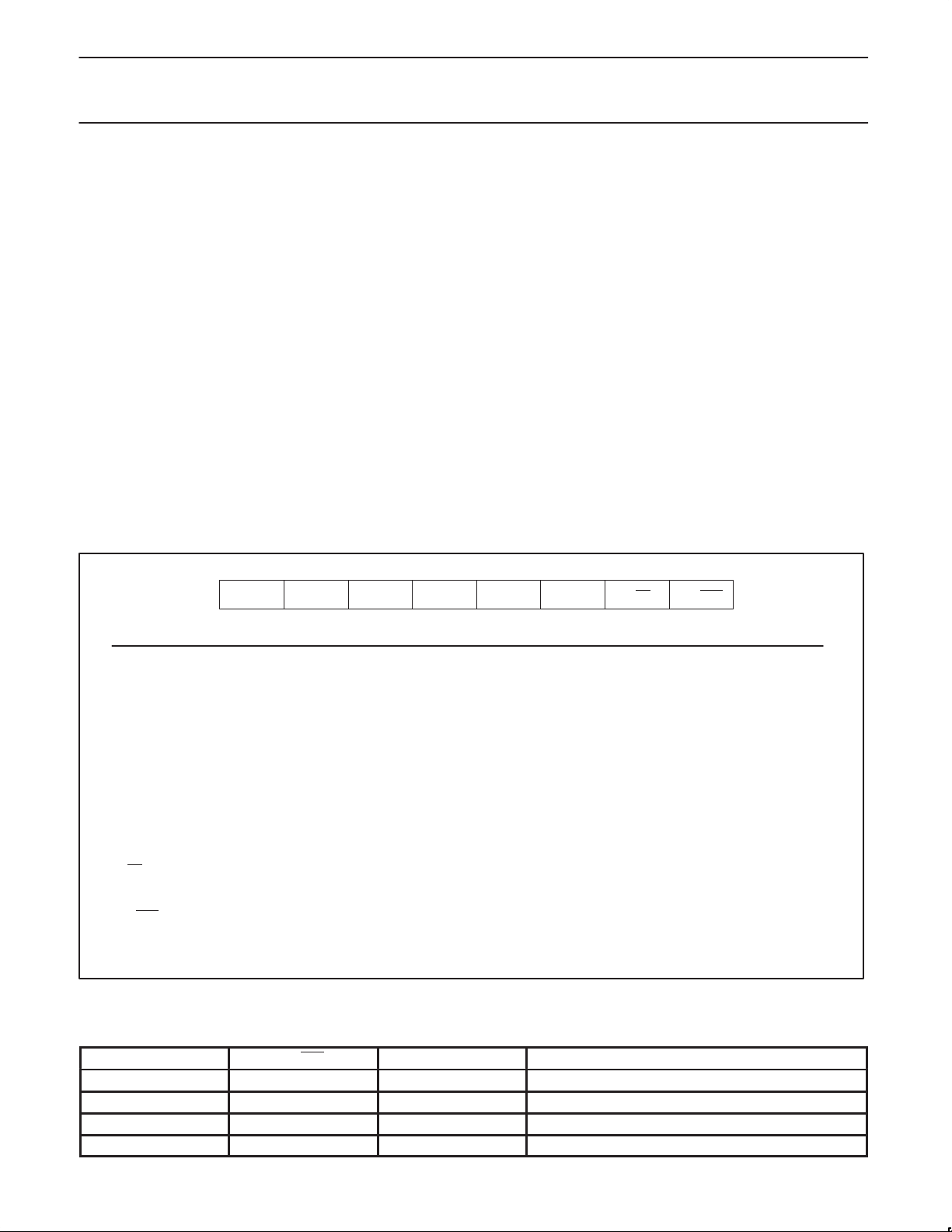
(MSB) (LSB)
TF2 EXF2 RCLK TCLK EXEN2 TR2 C/T2 CP/RL2
Symbol Position Name and Significance
TF2 T2CON.7 Timer 2 overflow flag set by a Timer 2 overflow and must be cleared by software. TF2 will not be set
EXF2 T2CON.6 Timer 2 external flag set when either a capture or reload is caused by a negative transition on T2EX and
RCLK T2CON.5 Receive clock flag. When set, causes the serial port to use Timer 2 overflow pulses for its receive clock
TCLK T2CON.4 Transmit clock flag. When set, causes the serial port to use T imer 2 overflow pulses for its transmit clock
EXEN2 T2CON.3 Timer 2 external enable flag. When set, allows a capture or reload to occur as a result of a negative
TR2 T2CON.2 Start/stop control for Timer 2. A logic 1 starts the timer.
C/T2
CP/RL2
T2CON.1 Timer or counter select. (Timer 2)
T2CON.0 Capture/Reload flag. When set, captures will occur on negative transitions at T2EX if EXEN2 = 1. When
EXEN2 = 1. When either RCLK = 1 or TCLK = 1, this bit is ignored and the timer is forced to auto-reload
when either RCLK or TCLK = 1.
EXEN2 = 1. When Timer 2 interrupt is enabled, EXF2 = 1 will cause the CPU to vector to the Timer 2
interrupt routine. EXF2 must be cleared by software.
in modes 1 and 3. RCLK = 0 causes Timer 1 overflow to be used for the receive clock.
in modes 1 and 3. TCLK = 0 causes Timer 1 overflows to be used for the transmit clock.
transition on T2EX if Timer 2 is not being used to clock the serial port. EXEN2 = 0 causes Timer 2 to
ignore events at T2EX.
0 = Internal timer (OSC/12)
1 = External event counter (falling edge triggered).
cleared, auto-reloads will occur either with Timer 2 overflows or negative transitions at T2EX when
on Timer 2 overflow .
Figure 1. Timer/Counter 2 (T2CON) Control Register
SU00866
Table 3. Timer 2 Operating Modes
RCLK + TCLK CP/RL2 TR2 MODE
0 0 1 16-bit Auto-reload
0 1 1 16-bit Capture
1 X 1 Baud rate generator
X X 0 (off)
1997 Jun 05
8
Page 9
Philips Semiconductors Preliminary specification
CMOS single-chip 8-bit microcontrollers
with FLASH program memory
OSC
T2 Pin
T2EX Pin
÷ 12
Transition
Detector
C/T2 = 0
C/T2
= 1
EXEN2
Control
TR2
Control
Capture
TL2
(8-bits)
RCAP2L RCAP2H
TH2
(8-bits)
89C535/89C536/89C538
TF2
Timer 2
Interrupt
EXF2
SU00066
OSC
T2 PIN
T2EX PIN
÷ 12
TRANSITION
DETECTOR
C/T2 = 0
= 1
C/T2
Figure 2. Timer 2 in Capture Mode
TL2
(8-BITS)
CONTROL
TR2
RELOAD
RCAP2L RCAP2H
CONTROL
EXEN2
Figure 3. Timer 2 in Auto-Reload Mode
TH2
(8-BITS)
TF2
EXF2
TIMER 2
INTERRUPT
SU00067
1997 Jun 05
9
Page 10
Philips Semiconductors Preliminary specification
Baud Rate
Osc Freq
CMOS single-chip 8-bit microcontrollers
with FLASH program memory
NOTE: OSC. Freq. is divided by 2, not 12.
OSC
T2 Pin
T2EX Pin
÷ 2
Transition
Detector
C/T2 = 0
C/T2
= 1
(8-bits)
Control
TR2
RCAP2L RCAP2H
EXF2
TL2
Timer 2
Interrupt
TH2
(8-bits)
89C535/89C536/89C538
Timer 1
Overflow
÷ 2
“0” “1”
“0”“1”
÷ 16
Reload
“0”“1”
÷ 16 TX Clock
SMOD
RCLK
RX Clock
TCLK
Control
EXEN2
Note availability of additional external interrupt.
Figure 4. Timer 2 in Baud Rate Generator Mode
Table 4. Timer 2 Generated Commonly Used
Baud Rates
Timer 2
RCAP2H RCAP2L
375K 12MHz FF FF
9.6K 12MHz FF D9
2.8K 12MHz FF B2
2.4K 12MHz FF 64
1.2K 12MHz FE C8
300 12MHz FB 1E
110 12MHz F2 AF
300 6MHz FD 8F
110 6MHz F9 57
Baud Rate Generator Mode
Bits TCLK and/or RCLK in T2CON (Table 3) allow the serial port
transmit and receive baud rates to be derived from either Timer 1 or
Timer 2. When TCLK= 0, Timer 1 is used as the serial port transmit
baud rate generator . When TCLK= 1, Timer 2 is used as the serial
port transmit baud rate generator. RCLK has the same effect for the
serial port receive baud rate. With these two bits, the serial port can
have different receive and transmit baud rates – one generated by
Timer 1, the other by Timer 2.
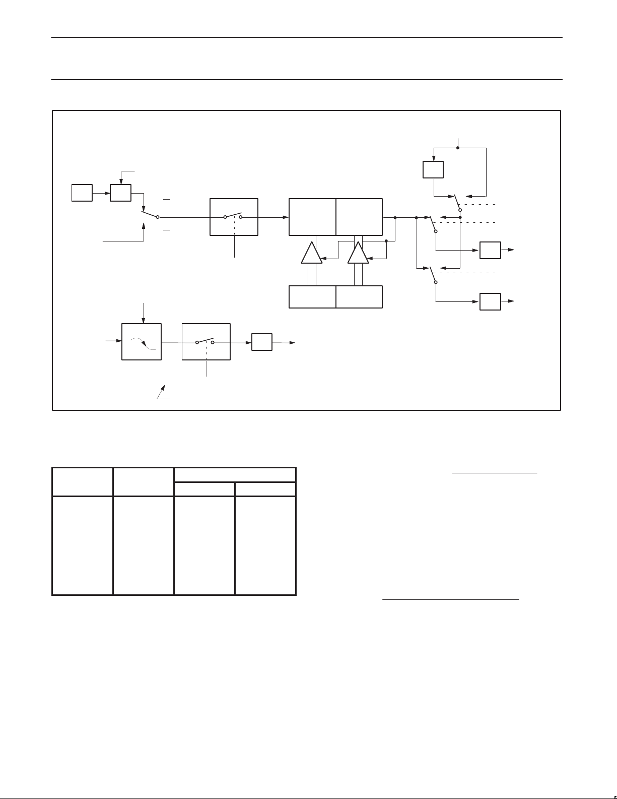
Figure 4 shows the Timer 2 in baud rate generation mode. The baud
rate generation mode is like the auto-reload mode,in that a rollover
in TH2 causes the Timer 2 registers to be reloaded with the 16-bit
value in registers RCAP2H and RCAP2L, which are preset by
software.
SU00068
The baud rates in modes 1 and 3 are determined by Timer 2’s
overflow rate given below:
Modes 1 and 3 Baud Rates
Timer 2 Overflow Rate
16
The timer can be configured for either “timer” or “counter” operation.
In many applications, it is configured for “timer” operation (C/T2*=0).
Timer operation is different for Timer 2 when it is being used as a
baud rate generator.
Usually, as a timer it would increment every machine cycle (i.e., 1/12
the oscillator frequency). As a baud rate generator, it increments
every state time (i.e., 1/2 the oscillator frequency). Thus the baud
rate formula is as follows:
Modes 1 and 3 Baud Rates =
Oscillator Frequency
[32 [65536 (RCAP2H,RCAP2L)]]
Where: (RCAP2H, RCAP2L)= The content of RCAP2H and
RCAP2L taken as a 16-bit unsigned integer.
The Timer 2 as a baud rate generator mode shown in Figure 4, is
valid only if RCLK and/or TCLK = 1 in T2CON register. Note that a
rollover in TH2 does not set TF2, and will not generate an interrupt.
Thus, the Timer 2 interrupt does not have to be disabled when
Timer 2 is in the baud rate generator mode. Also if the EXEN2
(T2 external enable flag) is set, a 1-to-0 transition in T2EX
(Timer/counter 2 trigger input) will set EXF2 (T2 external flag) but
will not cause a reload from (RCAP2H, RCAP2L) to (TH2,TL2).
Therefore when Timer 2 is in use as a baud rate generator, T2EX
can be used as an additional external interrupt, if needed.
1997 Jun 05
10
Page 11
Philips Semiconductors Preliminary specification
CMOS single-chip 8-bit microcontrollers
with FLASH program memory
When Timer 2 is in the baud rate generator mode, one should not try
to read or write TH2 and TL2. As a baud rate generator, T imer 2 is
incremented every state time (osc/2) or asynchronously from pin T2;
under these conditions, a read or write of TH2 or TL2 may not be
accurate. The RCAP2 registers may be read, but should not be
written to, because a write might overlap a reload and cause write
and/or reload errors. The timer should be turned off (clear TR2)
before accessing the Timer 2 or RCAP2 registers.
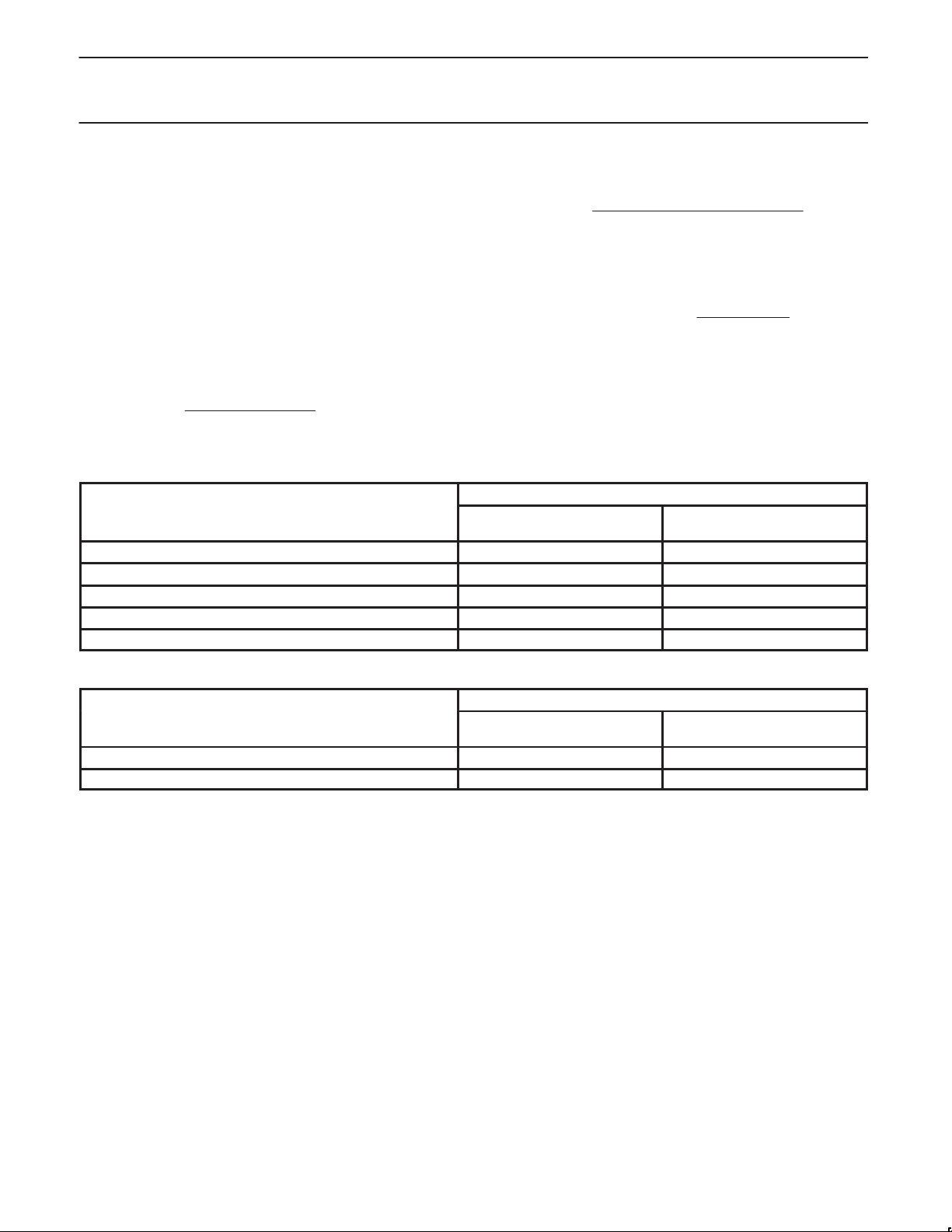
Table 4 shows commonly used baud rates and how they can be
obtained from Timer 2.
Summary Of Baud Rate Equations
Timer 2 is in baud rate generating mode. If Timer 2 is being clocked
through pin T2(P1.0) the baud rate is:
Baud Rate +
Timer 2 Overflow Rate
16
Table 5. Timer 2 as a Timer
MODE
16-bit Auto-Reload 00H 08H
16-bit Capture 01H 09H
Baud rate generator receive and transmit same baud rate 34H 36H
Receive only 24H 26H
Transmit only 14H 16H
If Timer 2 is being clocked internally , the baud rate is:
Baud Rate +
Where f
To obtain the reload value for RCAP2H and RCAP2L, the above
equation can be rewritten as:
= Oscillator Frequency
OSC
RCAP2H,RCAP2L + 65536 *
Timer/Counter 2 Set-up
Except for the baud rate generator mode, the values given for
T2CON do not include the setting of the TR2 bit. Therefore, bit TR2
must be set, separately, to turn the timer on. see Table 5 for set-up
of Timer 2 as a timer. Also see Table 6 for set-up of Timer 2 as a
counter.
INTERNAL CONTROL
(Note 1)
89C535/89C536/89C538
f
[32 [65536 * (RCAP2H,RCAP2L)]]
T2CON
OSC
f
ǒ
32 Baud Rate
EXTERNAL CONTROL
OSC
(Note 2)
Ǔ
Table 6. Timer 2 as a Counter
TMOD
MODE
16-bit 02H 0AH
Auto-Reload 03H 0BH
NOTES:
1. Capture/reload occurs only on timer/counter overflow.
2. Capture/reload occurs on timer/counter overflow and a 1-to-0 transition on T2EX (P1.1) pin except when Timer 2 is used in the baud rate
generator mode.
INTERNAL CONTROL
(Note 1)
EXTERNAL CONTROL
(Note 2)
1997 Jun 05
11
Page 12
Philips Semiconductors Preliminary specification
CMOS single-chip 8-bit microcontrollers
with FLASH program memory
Serial Interface
The 89C538/536 has a standard 80C51 serial port. This serial port
can operate in 4 modes:
Mode 0: Serial data enters and exits through RxD. TxD outputs the
shift clock. 8 bits are transmitted/received (LSB first). The baud rate
is fixed at 1/12 the oscillator frequency.
Mode 1: 10 bits are transmitted (through TxD) or received (through
RxD): a start bit (0), 8 data bits (LSB first), and a stop bit (1). On
receive, the stop bit goes into RB8 in Special Function Register
SCON. The baud rate is variable.
Mode 2: 11 bits are transmitted (throughTxD) or received (through
RxD): start bit (0), 8 data bits (LSB first), a programmable 9th data
bit, and a stop bit (1). On Transmit, the 9th data bit (TB8 in SCON)
can be assigned the value of 0 or 1, Or, for example, the parity bit
(P, in the PSW) could be moved into TB8. On receive, the 9th data
bit goes into RB8 in Special Function Register SCON, while the stop
bit is ignored. The baud rate is programmable to either 1/32 or 1/64
the oscillator frequency.
SCON Address = 98H
Bit Addressable
SM0 SM1 SM2 REN TB8 RB8 Tl Rl
Bit: 76543210
89C535/89C536/89C538
Mode 3: 11 bits are transmitted (through TxD) or received (through
jRxD): a start bit (0), 8 data bits (LSB first), a programmable 9th data
bit, and a stop bit (1). In fact, Mode 3 is the same as Mode 2 in all
respects except baud rate. The baud rate in Mode 3 is variable.
In all four modes, transmission is initiated by any instruction that
uses SBUF as a destination register. Reception is initiated in Mode 0
by the condition RI = 0 and REN = 1. Reception is initiated in the
other modes by the incoming start bit if REN = 1.
Serial Port Control Register
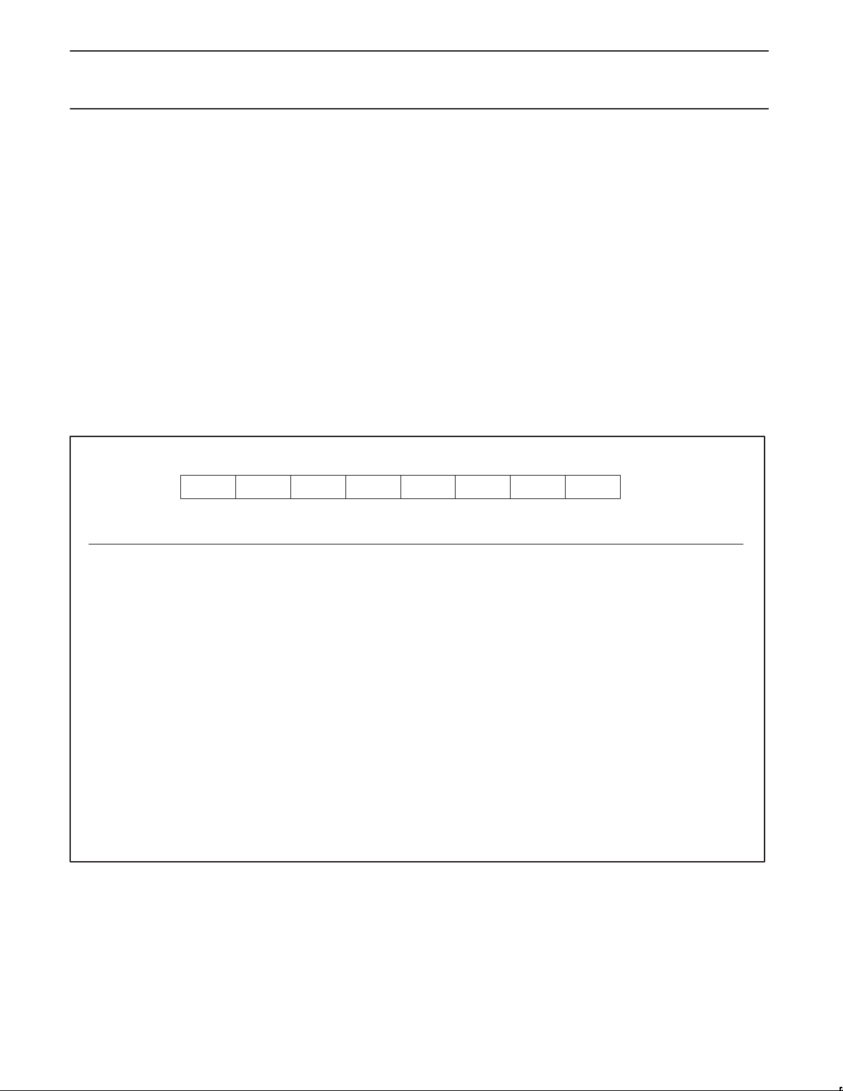
The serial port control and status register is the Special
FunctionRegister SCON, shown in Figure 5. This register contains
not only the mode selection bits, but also the 9th data bit for transmit
and receive (TB8 and RB8), and the serial port interrupt bits (TI and
RI).
Additional details of serial port operation may be found in the 80C51
Family Hardware Description found in the
8–Bit Microcontroller Data Handbook, IC20
Philips 80C51–Based
.
Reset Value = 0000 0000B
Symbol Function
SM0 Serial Port Mode Bit 0
SM1 Serial Port Mode Bit 1
SM2 Enables the Automatic Address Recognition feature in Modes 2 or 3. If SM2 = 1 then Rl will not be set unless the
REN Enables serial reception. Set by software to enable reception. Clear by software to disable reception.
TB8 The 9th data bit that will be transmitted in Modes 2 and 3. Set or clear by software as desired.
RB8 In modes 2 and 3, the 9th data bit that was received. In Mode 1, if SM2 = 0, RB8 is the stop bit that was received.
Tl Transmit interrupt flag. Set by hardware at the end of the 8th bit time in Mode 0, or at the beginning of the stop bit in the
Rl Receive interrupt flag. Set by hardware at the end of the 8th bit time in Mode 0, or halfway through the stop bit time in
NOTE:
**f
= oscillator frequency
OSC
SM0 SM1 Mode Description Baud Rate**
0 0 0 shift register f
0 1 1 8-bit UART variable
1 0 2 9-bit UART f
1 1 3 9-bit UART variable
received 9th data bit (RB8) is 1, indicating an address, and the received byte is a Given or Broadcast Address.
In Mode 1, if SM2 = 1 then Rl will not be activated unless a valid stop bit was received, and the received byte is a
Given or Broadcast Address. In Mode 0, SM2 should be 0.
In Mode 0, RB8 is not used.
other modes, in any serial transmission. Must be cleared by software.
the other modes, in any serial reception (except see SM2). Must be cleared by software.
Figure 5. SCON: Serial Port Control Register
OSC
OSC
/12
/64 or f
OSC
/32
SU00867
1997 Jun 05
12
Page 13
Philips Semiconductors Preliminary specification
INTERRUPT PRIORITY LEVEL
CMOS single-chip 8-bit microcontrollers
with FLASH program memory
Interrupt Priority Structure
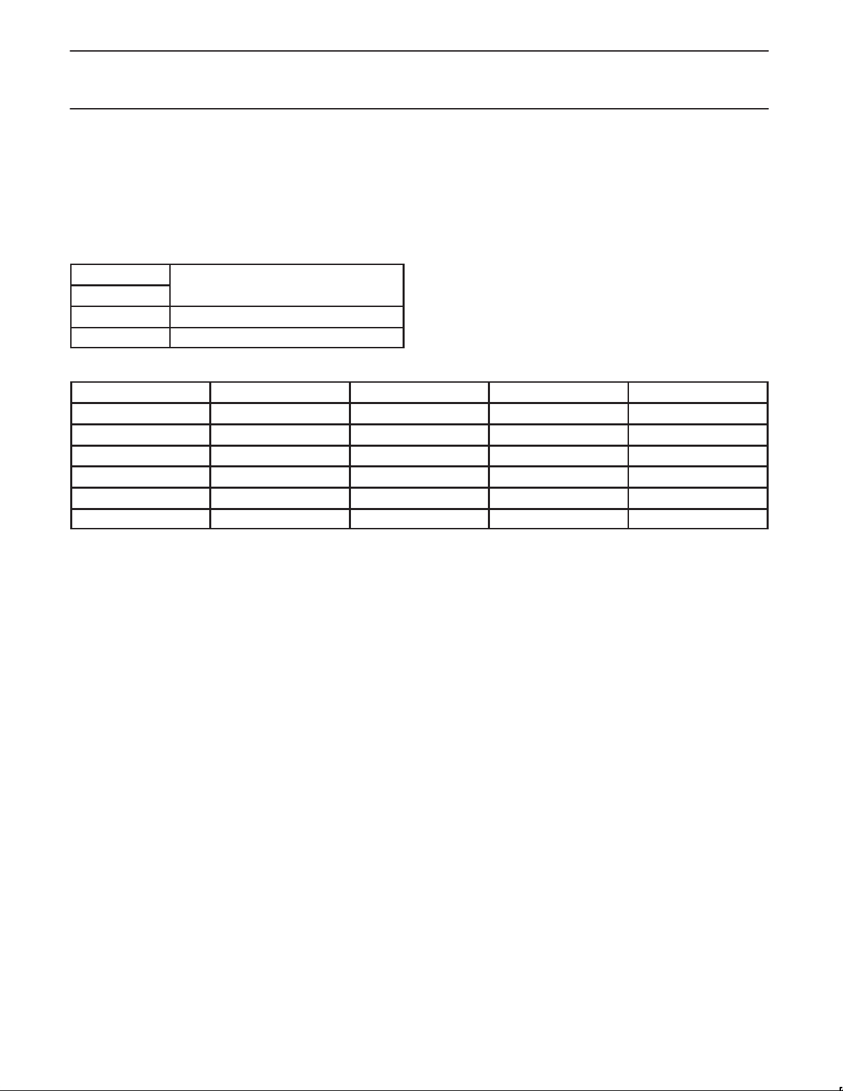
The 89C535/536/538 has a 6-source two-level interrupt structure
(see Table 7). There are 2 SFRs associated with the interrupts on
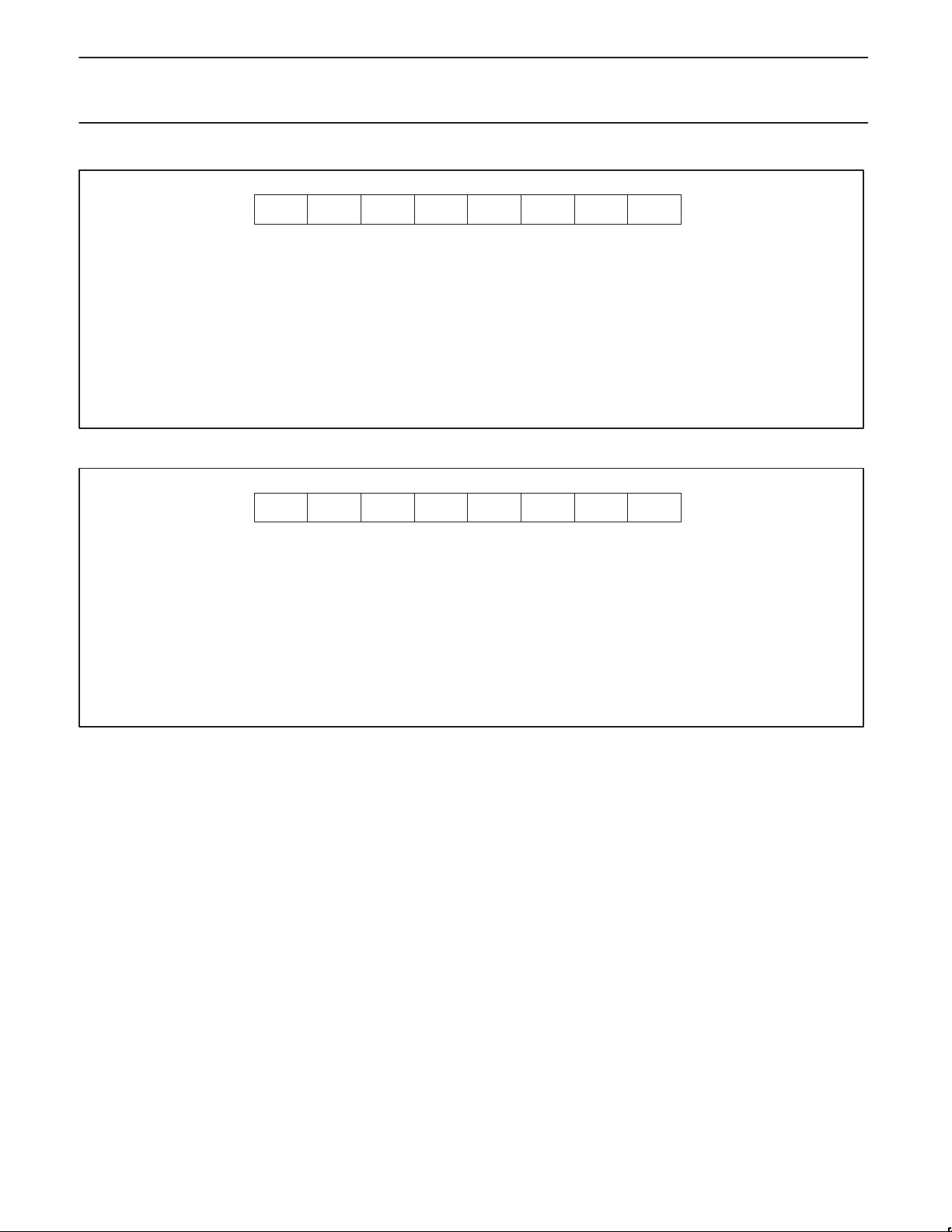
the 89C535/536/538. They are the IE and IP. (See Figures 6 and 7.)
The function of the IPH SFR is simple and when combined with the
IP SFR determines the priority of each interrupt. The priority of each
interrupt is determined as shown in the following table:
PRIORITY BITS
IP.x
0 Level 0 (lowest priority)
1 Level 1 (highest priority)
Table 7. Interrupt Table
SOURCE POLLING PRIORITY REQUEST BITS HARDWARE CLEAR? VECTOR ADDRESS
X0 1 IE0 N (L)1Y (T)
T0 2 TP0 Y 0BH
X1 3 IE1 N (L) Y (T) 13H
T1 4 TF1 Y 1BH
SP 5 R1, TI N 23H
T2 6 TF2, EXF2 N 2BH
NOTES:
1. L = Level activated
2. T = Transition activated
89C535/89C536/89C538
An interrupt will be serviced as long as an interrupt of equal or
higher priority is not already being serviced. If an interrupt of equal
or higher level priority is being serviced, the new interrupt will wait
until it is finished before being serviced. If a lower priority level
interrupt is being serviced, it will be stopped and the new interrupt
serviced. When the new interrupt is finished, the lower priority level
interrupt that was stopped will be completed.
2
03H
1997 Jun 05
13
Page 14
Philips Semiconductors Preliminary specification
CMOS single-chip 8-bit microcontrollers
with FLASH program memory
Enable Bit = 1 enables the interrupt.
Enable Bit = 0 disables it.
BIT SYMBOL FUNCTION
IE.7 EA Global disable bit. If EA = 0, all interrupts are disabled. If EA = 1, each interrupt can be individually
enabled or disabled by setting or clearing its enable bit.
IE.6 — Not implemented.
IE.5 ET2 Timer 2 interrupt enable bit.
IE.4 ES Serial Port interrupt enable bit.
IE.3 ET1 Timer 1 interrupt enable bit.
IE.2 EX1 External interrupt 1 enable bit.
IE.1 ET0 Timer 0 interrupt enable bit.
IE.0 EX0 External interrupt 0 enable bit.
Figure 6. IE Registers
89C535/89C536/89C538
01234567
ET0EX1ET1ESET2—EA
PT0PX1PT1PSPT2——
EX0IE (0A8H)
01234567
PX0IP (0B8H)
SU00571
Priority Bit = 1 assigns higher priority
Priority Bit = 0 assigns lower priority
BIT SYMBOL FUNCTION
IP.7 — Not implemented, reserved for future use.
IP.6 — Not implemented, reserved for future use.
IP.5 PT2 Timer 2 interrupt priority bit.
IP.4 PS Serial Port interrupt priority bit.
IP.3 PT1 Timer 1 interrupt priority bit.
IP.2 PX1 External interrupt 1 priority bit.
IP.1 PT0 Timer 0 interrupt priority bit.
IP.0 PX0 External interrupt 0 priority bit.
Figure 7. IP Registers
SU00572
1997 Jun 05
14
Page 15
Philips Semiconductors Preliminary specification
CMOS single-chip 8-bit microcontrollers
with FLASH program memory
Expanded Data RAM Addressing
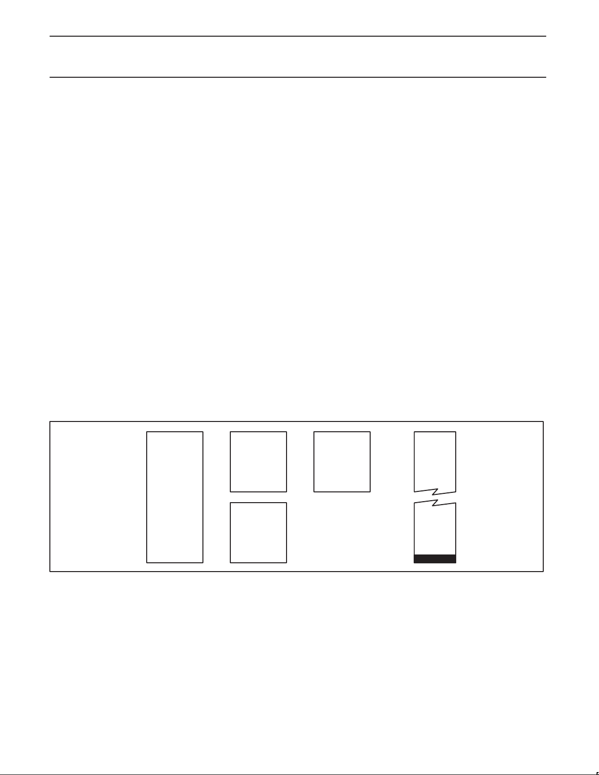
The 89C535/536/538 has internal data memory that is mapped into
four separate segments: the lower 128 bytes of RAM, upper 128
bytes of RAM, 128 byte s S pecial Func tion Regist er (SFR), and 256
bytes expanded RAM (ERAM).
The four segments are:
1. The Lower 128 bytes of RAM (addresses 00H to 7FH) are
directly and indirectly addressable.
2. The Upper 128 bytes of RAM (addresses 80H to FFH) are
indirectly addressable only.
3. The Special Function Registers, SFRs, (addresses 80H to FFH)
are directly addressable only.
4. The 256-bytes expanded RAM (ERAM, 00H – FFH) are indirectly
accessed by move external instruction, MOVX.
The Lower 128 bytes can be accessed by either direct or indirect
addressing. The Upper 128 bytes can be accessed by indirect
addressing only . The Upper 128 bytes occupy the same address
space as the SFRs. That means they have the same address, but
are physically separate from SFR space.
When an instruction accesses an internal location above address
7FH, the CPU knows whether the access is to the upper 128 bytes
of data RAM or to SFR space by the addressing mode used in the
instruction. Instructions that use direct addressing access SFR
space. For example:
MOV 0A0H,#data
accesses the SFR at location 0A0H (which is P2). Instructions that
use indirect addressing access the Upper 128 bytes of data RAM.
89C535/89C536/89C538
For example:
MOV @R0,#data
where R0 contains 0A0H, accesses the data byte at address 0A0H,
rather than P2 (whose address is 0A0H).
The ERAM can be accessed by indirect addressing and MOVX
instructions. This part of memory is physically located on-chip,
logically occupies the first 256-bytes of external data memory.
The ERAM is indirectly addressed, using the MOVX instruction in
combination with any of the registers R0, R1 of the selected bank or
DPTR. An access to ERAM will not affect ports P0, P3.6 (WR#) and
P3.7 (RD#). P2 SFR is output during external addressing.
For example,
MOVX @R0,#data
where R0 contains 0A0H, accesses the ERAM at address 0A0H
rather than external memory. An access to external data memory
locations higher than FFH (i.e., 0100H to FFFFH) will be performed
with the MOVX DPTR instructions in the same way as in the
standard 80C51, so with P0 and P2 as data/address bus, and P3.6
and P3.7 as write and read timing signals. Refer to Figure 8.
External data memory cannot be accessed using the MOVX with R0
or R1. This will always access the ERAM.
The stack pointer (SP) may be located anywhere in the 256 bytes
RAM (lower and upper RAM) internal data memory. The stack may
not be located in the ERAM.
FF
ERAM
256 BYTES
00
FF
UPPER
128 BYTES
INTERNAL RAM
80 80
LOWER
128 BYTES
INTERNAL RAM
00
FF
SPECIAL
FUNCTION
REGISTER
00
FFFF
0100
0000
EXTERNAL
DATA
MEMORY
SU00868
Figure 8. Internal and External Data Memory Address Space
1997 Jun 05
15
Page 16
Philips Semiconductors Preliminary specification
CMOS single-chip 8-bit microcontrollers
with FLASH program memory
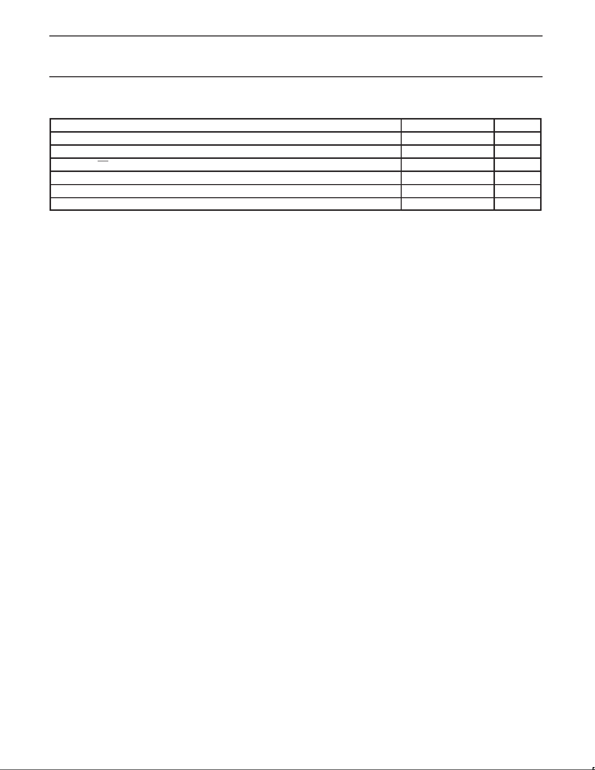
ABSOLUTE MAXIMUM RATINGS
Operating temperature under bias 0 to +70 °C
Storage temperature range –65 to +150 °C
Voltage on EA/VPP pin to V
Voltage on any other pin to V
Maximum IOL per I/O pin 15 mA
Power dissipation (based on package heat transfer limitations, not device power consumption) 1 W
NOTES:
1. Stresses above those listed under Absolute Maximum Ratings may cause permanent damage to the device. This is a stress rating only and
functional operation of the device at these or any conditions other than those described in the AC and DC Electrical Characteristics section
of this specification is not implied.
2. This product includes circuitry specifically designed for the protection of its internal devices from the damaging effects of excessive static
charge. Nonetheless, it is suggested that conventional precautions be taken to avoid applying greater than the rated maxima.
3. Parameters are valid over operating temperature range unless otherwise specified. All voltages are with respect to V
noted.
SS
SS
1, 2, 3
PARAMETER
89C535/89C536/89C538
RATING UNIT
0 to +13.0 V
–0.5 to +6.5 V
unless otherwise
SS
1997 Jun 05
16
Page 17
Philips Semiconductors Preliminary specification
SYMBOL
PARAMETER
UNIT
CMOS single-chip 8-bit microcontrollers
with FLASH program memory
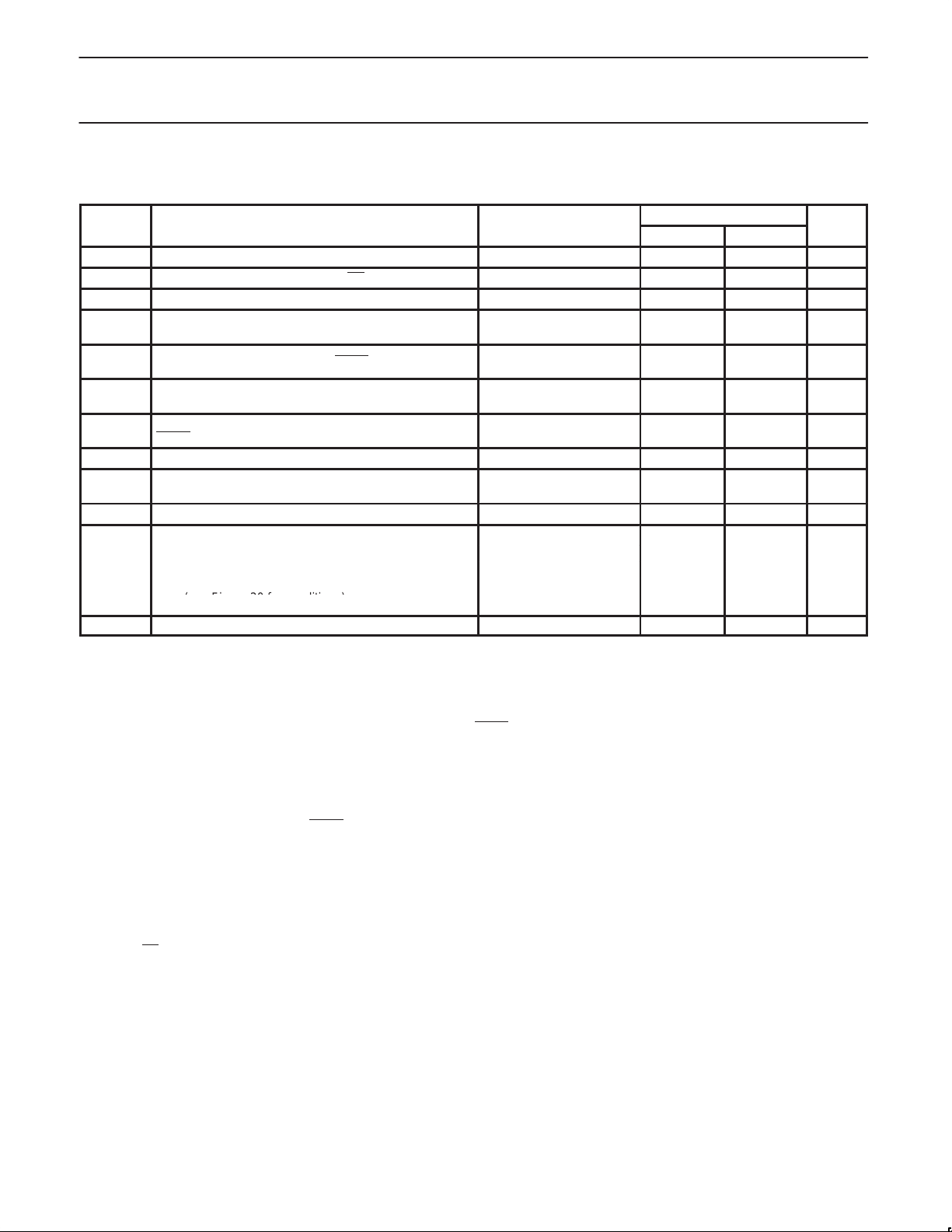
DC ELECTRICAL CHARACTERISTICS
T
= 0°C to +70°C; 5V ±10%; VSS = 0V
amb
V
IL
V
IH
V
IH1
V
OL
V
OL1
V
OH
V
OH1
I
IL
I
TL
I
LI
I
CC
Input low voltage 4.5V < VCC < 5.5V –0.5 0.2VCC–0.1 V
Input high voltage (ports 0, 1, 2, 3, EA) 0.2VCC+0.9 VCC+0.5 V
Input high voltage, XTAL1, RST 0.7V
Output low voltage, ports 1, 2, 3
Output low voltage, port 0, ALE, PSEN
Output high voltage, ports 1, 2, 3
Output high voltage (port 0 in external bus mode), ALE7,
2
PSEN
6
5, 6
2
Logical 0 input current, ports 1, 2, 3 VIN = 0.4V –1 –50 µA
Logical 1-to-0 transition current, ports 1, 2, 3
Input leakage current, port 0 0.45 < VIN < VCC – 0.3 ±10 µA
Power supply current (see Figure 16): See note 4
Active mode VCC = 5.5V 60 mA
Idle mode FREQ = 24 MHz 25 mA
Power-down mode or clock stopped
(see Figure 20 for conditions)
89C535/89C536/89C538
TEST
CONDITIONS
VCC = 4.5V
= 1.6mA
I
OL
VCC = 4.5V
= 3.2mA
I
OL
VCC = 4.5V
I
OH
VCC = 4.5V
= –800µA
I
OH
= –30µA
1
1
VCC – 0.7 V
VCC – 0.7 V
VIN = 2.0V
See note 3
T
= 0°C to 70°C 100 µA
amb
LIMITS
MIN MAX
CC
VCC+0.5 V
0.4 V
0.4 V
–650 µA
R
RST
Internal reset pull-down resistor 40 225 kΩ
NOTES:
1. Capacitive loading on ports 0 and 2 may cause spurious noise to be superimposed on the V
to external bus capacitance discharging into the port 0 and port 2 pins when these pins make 1-to-0 transitions during bus operations. In the
s of ALE and ports 1 and 3. The noise is due
OL
worst cases (capacitive loading > 100pF), the noise pulse on the ALE pin may exceed 0.8V . In such cases, it may be desirable to qualify
ALE with a Schmitt Trigger, or use an address latch with a Schmitt Trigger STROBE input. I
single output sinks more than 5mA and no more than two outputs exceed the test conditions.
2. Capacitive loading on ports 0 and 2 may cause the V
address bits are stabilizing.
on ALE and PSEN to momentarily fall below the VCC–0.7 specification when the
OH
can exceed these conditions provided that no
OL
3. Pins of ports 1, 2 and 3 source a transition current when they are being externally driven from 1 to 0. The transition current reaches its
maximum value when V
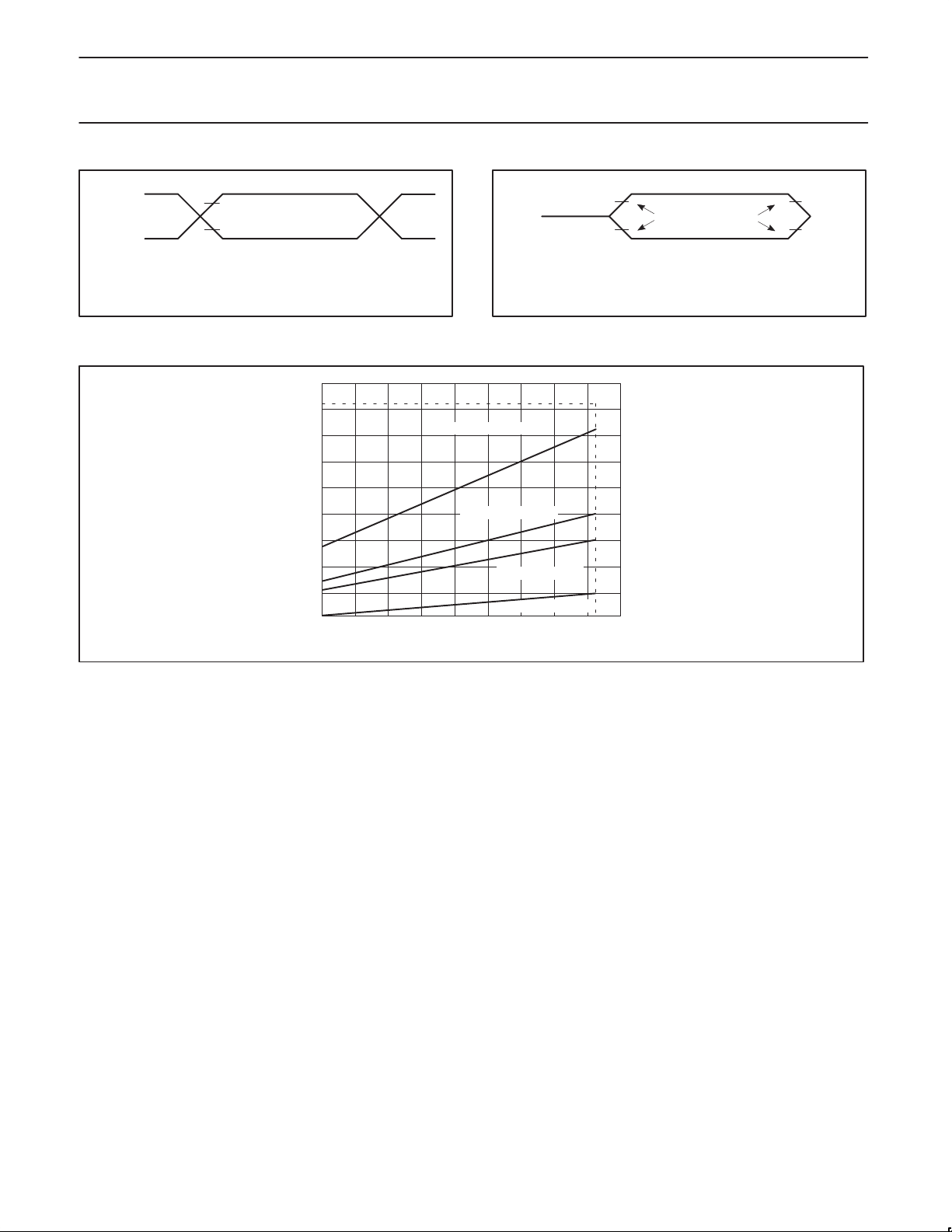
4. See Figures 17 through 20 for I
Active mode: I
Idle mode: I
5. Load capacitance for port 0, ALE, and PSEN
6. Under steady state (non-transient) conditions, I
Maximum I
Maximum I
Maximum total I
exceeds the test condition, VOL may exceed the related specification. Pins are not guaranteed to sink current greater than the listed
If I
OL
test conditions.
per port pin: 15mA
OL
per 8-bit port: 26mA
OL
7. ALE is tested to V
8. Pin capacitance is characterized but not tested. Pin capacitance is less than 25pF. Pin capacitance of ceramic package is less than 15pF
(except EA
is 25pF).
is approximately 2V .
IN
CC(MAX)
CC(MAX)
for all outputs: 71mA
OL
, except when ALE is off then VOH is the voltage specification.
OH1
test conditions.
CC
= 0.9 × FREQ. + 1.1mA
= 0.18 × FREQ. +1.0mA; See Figure 16.
= 100pF, load capacitance for all other outputs = 80pF.
must be externally limited as follows:
OL
1997 Jun 05
17
Page 18
Philips Semiconductors Preliminary specification
CMOS single-chip 8-bit microcontrollers
with FLASH program memory
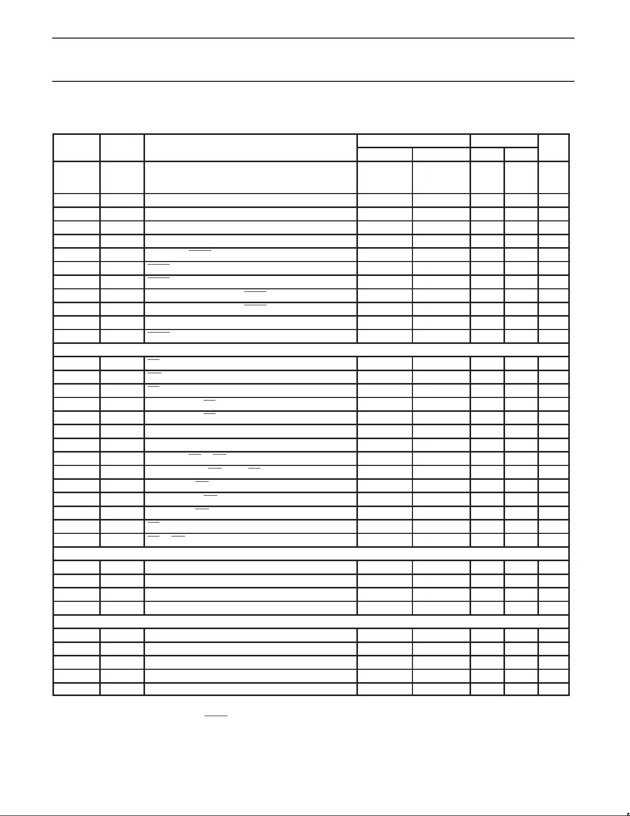
AC ELECTRICAL CHARACTERISTICS
T
= 0°C to +70°C, VCC = 5V ±10%, VSS = 0V
amb
SYMBOL FIGURE PARAMETER MIN MAX MIN MAX UNIT
1/t
CLCL
t
LHLL
t
AVLL
t
LLAX
t
LLIV
t
LLPL
t
PLPH
t
PLIV
t
PXIX
t
PXIZ
t
AVIV
t
PLAZ
Data Memory
t
RLRH
t
WLWH
t
RLDV
t
RHDX
t
RHDZ
t
LLDV
t
AVDV
t
LLWL
t
AVWL
t
QVWX
t
WHQX
t
QVWH
t
RLAZ
t
WHLH
External Clock
t
CHCX
t
CLCX
t
CLCH
t
CHCL
Shift Register
t
XLXL
t
QVXH
t
XHQX
t
XHDX
t
XHDV
NOTES:
1. Parameters are valid over operating temperature range unless otherwise specified.
2. Load capacitance for port 0, ALE, and PSEN
3. Interfacing the microcontroller to devices with float times up to 45ns is permitted. This limited bus contention will not cause damage to Port 0
drivers.
9 Oscillator frequency
Speed versions : N (33MHz)
9 ALE pulse width 2t
9 Address valid to ALE low t
9 Address hold after ALE low t
9 ALE low to valid instruction in 4t
9 ALE low to PSEN low t
9 PSEN pulse width 3t
9 PSEN low to valid instruction in 3t
9 Input instruction hold after PSEN 0 0 ns
9 Input instruction float after PSEN t
9 Address to valid instruction in 5t
9 PSEN low to address float 10 10 ns
10, 11 RD pulse width 6t
10, 11 WR pulse width 6t
10, 11 RD low to valid data in 5t
10, 11 Data hold after RD 0 0 ns
10, 11 Data float after RD 2t
10, 11 ALE low to valid data in 8t
10, 11 Address to valid data in 9t
10, 11 ALE low to RD or WR low 3t
10, 11 Address valid to WR low or RD low 4t
10, 11 Data valid to WR transition t
10, 11 Data hold after WR t
11 Data valid to WR high 7t
10, 11 RD low to address float 0 0 ns
10, 11 RD or WR high to ALE high t
13 High time 17 t
13 Low time 17 t
13 Rise time 5 ns
13 Fall time 5 ns
12 Serial port clock cycle time 12t
12 Output data setup to clock rising edge 10t
12 Output data hold after clock rising edge 2t
12 Input data hold after clock rising edge 0 0 ns
12 Clock rising edge to input data valid 10t
1, 2, 3
CLCL
CLCL
CLCL
CLCL
CLCL
CLCL
CLCL
CLCL
CLCL
CLCL
CLCL
CLCL
CLCL
CLCL
CLCL
= 100pF, load capacitance for all other outputs = 80pF.
89C535/89C536/89C538
VARIABLE CLOCK 33MHz CLOCK
3.5 33
3.5 33
–40 21 ns
–25 5 ns
–25 5 ns
–65 55 ns
CLCL
–25 5 ns
–45 45 ns
–60 30 ns
CLCL
–25 5 ns
CLCL
–80 70 ns
CLCL
–100 82 ns
–100 82 ns
–90 60 ns
CLCL
–28 32 ns
CLCL
–150 90 ns
CLCL
–165 105 ns
CLCL
–50 3t
–75 45 ns
–30 0 ns
–25 5 ns
–130 80 ns
–25 t
CLCL
–133 167 ns
–80 50 ns
+50 40 140 ns
CLCL
+25 5 55 ns
CLCL
CLCL–tCLCX
CLCL–tCHCX
360 ns
–133 167 ns
CLCL
MHz
ns
ns
1997 Jun 05
18
Page 19
Philips Semiconductors Preliminary specification
CMOS single-chip 8-bit microcontrollers
with FLASH program memory
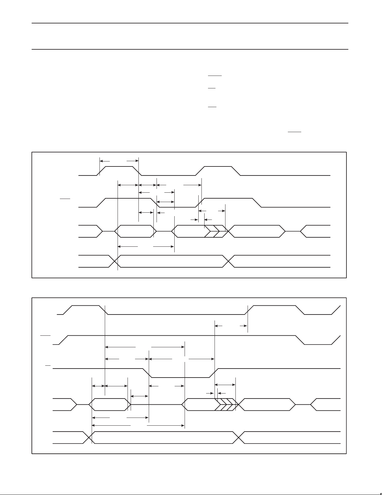
EXPLANATION OF THE AC SYMBOLS
Each timing symbol has five characters. The first character is always
‘t’ (= time). The other characters, depending on their positions,
indicate the name of a signal or the logical status of that signal. The
designations are:
A – Address
C – Clock
D – Input data
H – Logic level high
I – Instruction (program memory contents)
L – Logic level low, or ALE
t
ALE
PSEN
PORT 0
LHLL
t
t
AVLL
LLPL
t
LLAX
A0–A7 A0–A7
t
LLIV
t
PLIV
t
PLPH
t
PLAZ
t
PXIX
INSTR IN
89C535/89C536/89C538
P – PSEN
Q – Output data
R–RD
signal
t – Time
V – Valid
W– WR
signal
X – No longer a valid logic level
Z – Float
Examples: t
t
PXIZ
= Time for address valid to ALE low.
AVLL
t
=Time for ALE low to PSEN low.
LLPL
ALE
PSEN
PORT 0
PORT 2
RD
PORT 2
t
AVLL
t
LLAX
A0–A7
FROM RI OR DPL
t
AVWL
t
AVIV
A0–A15 A8–A15
Figure 9. External Program Memory Read Cycle
t
WHLH
t
LLDV
t
LLWL
t
RLAZ
t
AVDV
P2.0–P2.7 OR A8–A15 FROM DPF A0–A15 FROM PCH
t
RLDV
t
RLRH
t
RHDZ
t
RHDX
DATA IN A0–A7 FROM PCL INSTR IN
SU00006
1997 Jun 05
SU00025
Figure 10. External Data Memory Read Cycle
19
Page 20
Philips Semiconductors Preliminary specification
CMOS single-chip 8-bit microcontrollers
with FLASH program memory
ALE
PSEN
t
WLWH
t
QVWH
DATA OUT A0–A7 FROM PCL INSTR IN
WR
PORT 0
PORT 2
t
AVLL
t
t
LLAX
A0–A7
FROM RI OR DPL
t
AVWL
LLWL
t
QVWX
P2.0–P2.7 OR A8–A15 FROM DPF A0–A15 FROM PCH
t
WHLH
t
89C535/89C536/89C538
WHQX
INSTRUCTION
ALE
CLOCK
OUTPUT DATA
WRITE TO SBUF
INPUT DATA
CLEAR RI
SU00026
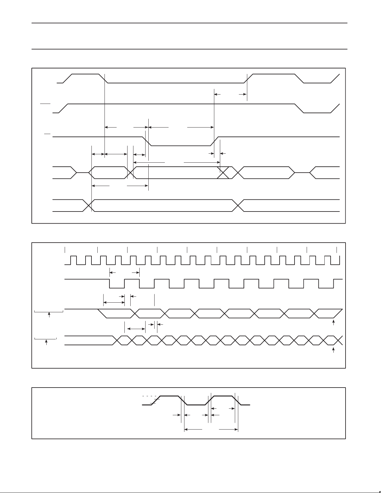
Figure 11. External Data Memory Write Cycle
012345678
t
XLXL
t
t
QVXH
t
XHDV
VALID VALID VALID VALID VALID VALID VALID VALID
XHQX
1230 4567
t
XHDX
SET TI
SET RI
SU00027
Figure 12. Shift Register Mode Timing
VCC–0.5
0.45V
0.7V
CC
0.2VCC–0.1
t
CHCL
t
CLCX
t
CHCX
t
CLCH
1997 Jun 05
t
CLCL
Figure 13. External Clock Drive
20
SU00009
Page 21
Philips Semiconductors Preliminary specification
CMOS single-chip 8-bit microcontrollers
with FLASH program memory
VCC–0.5
0.45V
NOTE:
AC inputs during testing are driven at VCC –0.5 for a logic ‘1’ and 0.45V for a logic ‘0’.
Timing measurements are made at VIH min for a logic ‘1’ and VIL max for a logic ‘0’.
Figure 14. AC Testing Input/Output
0.2V
0.2V
CC
CC
+0.9
–0.1
(mA)
CC
I
90.00
80.00
70.00
60.00
50.00
40.00
30.00
20.00
10.00
0.00
SU00717
0
481216
MAX ACTIVE MODE
FREQ AT XTAL1 (MHz)
89C535/89C536/89C538
V
+0.1V
V
NOTE:
For timing purposes, a port is no longer floating when a 100mV change from
load voltage occurs, and begins to float when a 100mV change from the loaded
V
OH/VOL
LOAD
LOAD
–0.1V
V
LOAD
level occurs. IOH/IOL ≥ ±20mA.
Figure 15. Float Waveform
TYP ACTIVE MODE
MAX IDLE MODE
TYP IDLE MODE
20 24 28 32 36
TIMING
REFERENCE
POINTS
–0.1V
V
OH
V
+0.1V
OL
SU00718
SU00886
Figure 16. ICC vs. FREQ Valid only within frequency specifications of the device under test
1997 Jun 05
21
Page 22
Philips Semiconductors Preliminary specification
CMOS single-chip 8-bit microcontrollers
with FLASH program memory
V
CC
I
CC
V
CC
V
CC
RST
(NC)
CLOCK SIGNAL
XTAL2
XTAL1
V
SS
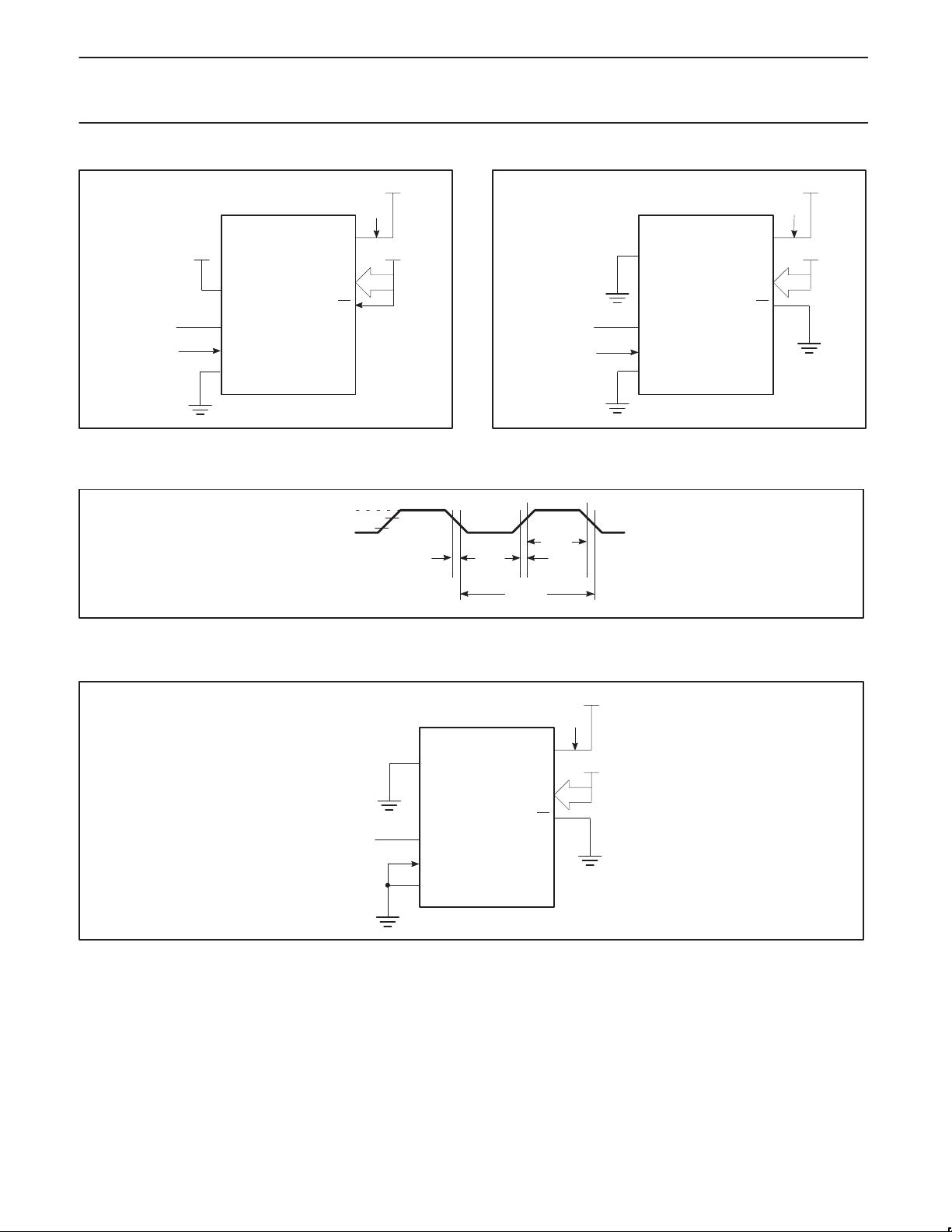
Figure 17. ICC Test Condition, Active Mode
All other pins are disconnected
VCC–0.5
0.45V
P0
EA
V
CC
SU00719
0.7V
0.2VCC–0.1
t
CHCL
CC
t
CLCX
89C535/89C536/89C538
RST
(NC)
CLOCK SIGNAL
Figure 18. ICC Test Condition, Idle Mode
All other pins are disconnected
t
CHCX
t
CLCH
XTAL2
XTAL1
V
SS
V
CC
I
CC
V
CC
V
CC
P0
EA
SU00720
t
CLCL
Figure 19. Clock Signal Waveform for ICC Tests in Active and Idle Modes
(NC)
t
CLCH
RST
XTAL2
XTAL1
V
= t
SS
CHCL
= 5ns
V
CC
I
CC
V
CC
V
CC
P0
EA
Figure 20. ICC Test Condition, Power Down Mode
All other pins are disconnected. V
= 2V to 5.5V
CC
SU00009
SU00016
1997 Jun 05
22
Page 23

Philips Semiconductors Preliminary specification
CMOS single-chip 8-bit microcontrollers
with FLASH program memory
FLASH EPROM PROGRAM MEMORY
FEATURES
•8K (89C535), 16K (89C536), 64K (89C538) or electrically
erasable internal program.
•Up to 64 Kilobyte external program memory if the internal program
memory is switched off (EA
•Programming and erasing voltage 12V 5%
•Command register architecture
– Byte Programming (10 us typical)
– Auto chip erase 5 seconds typical (including preprogramming
time)
•Auto Erase and auto program
polling
– DATA
– Toggle bit
•100 minimum erase/program cycles
•Advanced CMOS FLASH EPROM memory technology
GENERAL DESCRIPTION
The 89C535/536/538 FLASH EPROM memory augments EPROM
functionality with In–circuit electrical erasure and programming. The
89C535/536/538 uses a command register to manage this
functionality .
The FLASH EPROM reliably stores memory contents even after 100
erase and program cycles. The cell is designed to optimize the
erase and programming mechanisms. In addition, the combination
of advanced tunnel oxide processing and low internal electric fields
for erase and programming operations produces reliable cycling.
The 89C535/536/538 uses a 12.0V 5%V
Auto Program/Erase algorithms.
Automatic Programming
The 89C535/536/538 is byte programmable using the Automatic
Programming algorithm. The Automatic Programming algorithm
= 0)..
supply to perform the
PP
89C535/89C536/89C538
does not require the system to time out or verify the data
programmed. The typical room temperature chip programming time
of the 89C535/536/538 is less than 5 seconds.
Automatic Chip Erase
The device may be erased using the automatic Erase algorithm. The
automatic Erase algorithm automatically programs the entire array
prior to electrical erase. The timing and verification of electrical
erase are controlled internal to the device.
Automatic Programming Algorithm
The 89C535/536/538 automatic Programming algorithm requires the
user to only write a program set–up command and a program
command (program data and address). The device automatically
times the programming pulse width, provides the program verify, and
counts the number of sequences. A status bit similar to DATA
polling and a status bit toggling between consecutive read cycles,
provide feedback to the user as to the status of the programming
operation.
AUTOMATIC ERASE ALGORITHM
The 89C535/536/538 Automatic Erase algorithm requires the user to
only write an erase set–up command and erase command. The
device will automatically pre–program and verify the entire array.
Then the device automatically times the erase pulse width, provides
the erase verify, and counts the number of sequences. A status bit
similar to DATA
consecutive read cycles, provide feedback to the user as to the
status of the erase operation.
Commands are written to the command register. Register contents
serve as inputs to an internal state–machine which controls the
erase and programming circuitry. During write cycles, the command
register internally latches address and data needed for the
programming and erase operations. For system design
simplification, the 89C535/536/538 is designed to support either WE
or CE controlled writes. During a system write cycle, addresses are
latched on the falling edge of WE
is latched on the rising edge of WE
simplify the following discussion, the WE
cycle control pin through the rest of this text. All setup and hold
times are with respect to the WE
polling and a status bit toggling between
or CE, whichever occurs last. Data
or CE, whichever occurs first. To
pin is used as the write
signal.
1997 Jun 05
23
Page 24
Philips Semiconductors Preliminary specification
CMOS single-chip 8-bit microcontrollers
with FLASH program memory
A0–A7
1
CE
4–6 MHz
P1
RST
P3.3
89C535/536/538
XTAL2
XTAL1
VSS
P2.6, P3.7, P3.1, P3.0
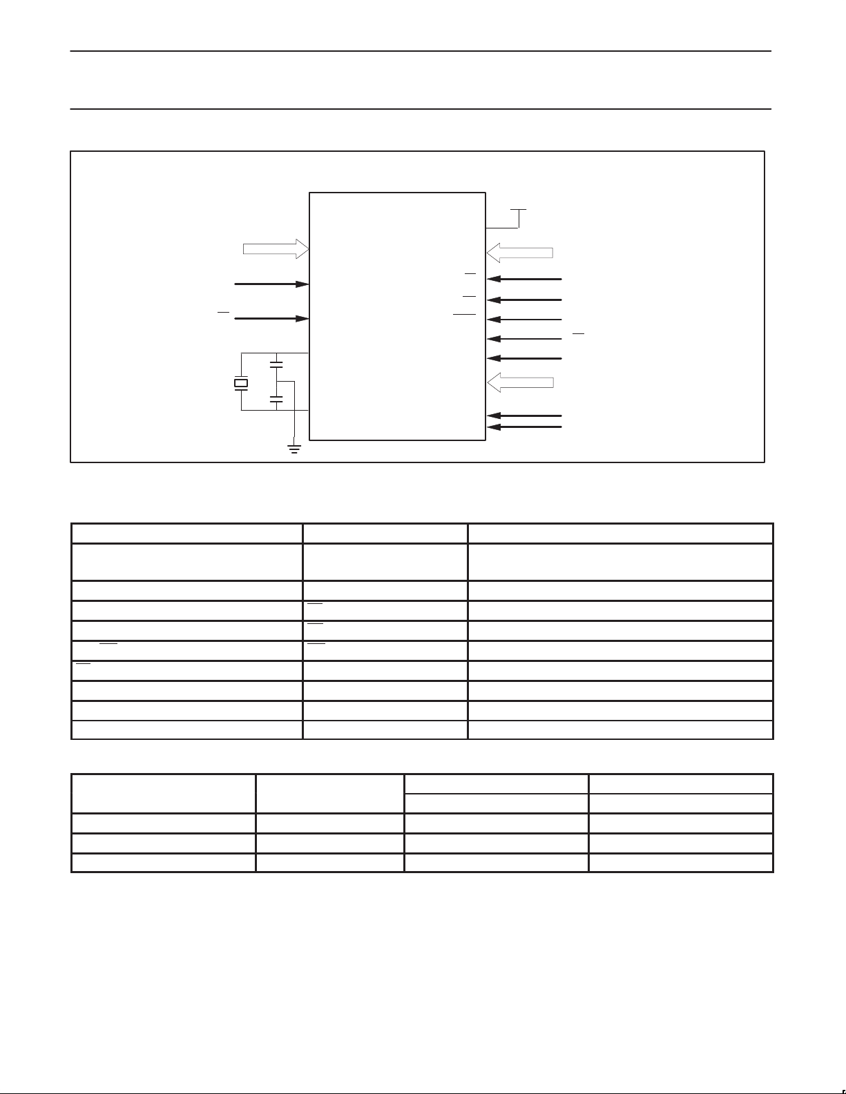
Figure 21. Erase/Programming/V erification
VDD
EA
ALE/WE
PSEN
P2.7
P3.5
P2.0–P2.5
P3.4
89C535/89C536/89C538
+5V
P0
PGM COMMAND/DATA
V
PP
LOW PULSE
0
OE
A15
A8–A13
A14
0000b
su00876
Table 8. Pin Description
PIN NAME SYMBOL FUNCTION
P1.0–P1.7
P2.0–P2.5, P3.4, P3.5
A0–A7
A8–A13, A14–A15
Input Low Order Address Bits
Input High Order Address Bits
P0.0–P0.7 Q0–Q7 Data Input/Output
P3.3 CE Chip Enable Input
P2.7 OE Output Enable Input
ALE/WE WE Write Enable Pin
EA V
PP
Program Supply Voltage
P2.6, P3.7, P3.1, P3.0 FTEST3–FTEST0 Flash T est Mode Selection
V
CC
V
CC
Power Supply Voltage (+5V)
GND GND Ground Pin
Table 9. Command Definitions
FIRST BUS CYCLE SECOND BUS CYCLE
COMMAND BUS CYCLES
Setup auto erase/auto erase (chip) 2 Write X 30H Write X 30H
Setup auto program/program 2 Write X 40H Write PA PD
Reset 2 Write X FFH Write X FFH
Note:
•PA = Address of memory location to be programmed
•PD = Data to be programmed at location
OPERATION ADDRESS DATA OPERATION ADDRESS DATA
Command Definitions
When low voltage is applied to the VPP pin, the contents of the
command register default to 00H. Placing high voltage on the V
pin enables read/write operations. Device operations are selected
by writing specific data patterns into the command register. Table 2
defines these 89C535/536/538 register commands. Table 3 defines
the bus operations of 89C535/536/538.
PP
1997 Jun 05
24
Page 25
Philips Semiconductors Preliminary specification
CMOS single-chip 8-bit microcontrollers
with FLASH program memory
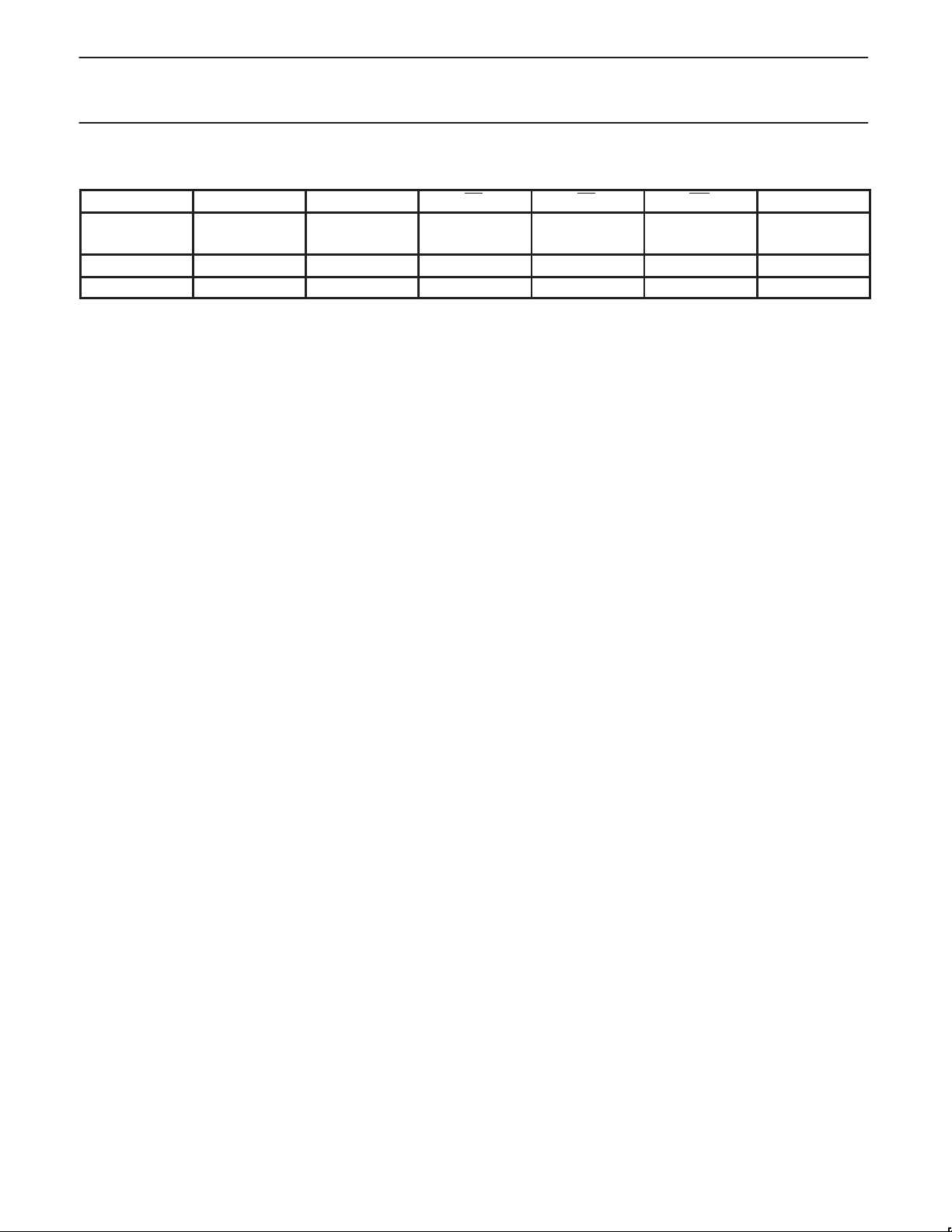
Table 10.
OPERATION VPP(1) CE OE WE D00–D07
READ/WRITE
Read(2) V
Standby(4) V
Write V
NOTES:
1. V
2. Read operation withVPP = V
3. With V
4. Refer to T able 38 for valid Data–In during a write operation.
5. X can be V
is the programming voltage specified for the device.
PPH
at high voltage, the standby current equals ICC+IPP (standby).
PP
or VIH.
IL
PPH
PPH
PPH
PPH
may access array data (if write command is preceded) or silicon ID codes.
Set–Up Automatic Chip Erase/Erase Commands
The automatic chip erase does not require the device to be entirely
pre–programmed prior to executing the Automatic set–up erase
command and automatic chip erase command. Upon executing the
Automatic chip erase command, the device automatically will
program and verify the entire memory for an all–zero data pattern.
When the device is automatically verified to contain an all–zero
pattern, a self–timed chip erase and verify begins. The erase and
verify operations are complete when the data on DQ7 is”1” at which
time the device returns to the standby mode. The system is not
required to provide any control or timing during these operations.
When using the Automatic Chip Erase algorithm, note that the erase
automatically terminates when adequate erase margin has been
achieved for the memory array (no erase verify command is
required). The margin voltages are internally generated in the same
manner as when the standard erase verify command is used.
The Automatic set–up erase command is a command only operation
that stages the device for automatic electrical erasure of all bytes in
the array. Automatic set–up erase is performed by writing 30H to the
command register.
To command automatic chip erase, the command 30H must be
written again to the command register. The automatic chip erase
begins on the rising edge of the WE and terminates when the data
on DQ7 is ”1 “ and the data on DQ6 stops toggling for two
consecutive read cycles, at which time the device returns to the
standby mode.
Set–Up Automatic Program/Program Commands
The Automatic Set–up Program is a command–only operation that
stages the devices for automatic programming. Automatic Set–up
Program is performed by writing 40H to the command register.
Once the Automatic Set–up Program operation is performed, the
next WE pulse causes a transition to an active programming
operation. Addresses are internally latched on the falling edge of the
WE pulse. Data is internally latched on the rising edge of the WE
pulse. The rising edge of WE also begins the programming
operation. The system is not required to provide further controls or
timings. The device will automatically provide an adequate internally
generated program pulse and verify margin. The automatic
programming operation is completed when the data read on DQ6
stops toggling for two consecutive read cycles and the data on DQ7
and DQ6 are equivalent to data written to these two bits at which
time the device returns to the Read mode (no program verify
command is required; but data can be read out if OE is active low).
V
IL
V
IH
V
IL
V
IL
X X Tri–State
V
IH
Reset Command
A reset command is provided as a means to safely abort the erase–
or program–command sequences. Following either set–up
command (erase or program) with two consecutive writes of FFH
will safely abort the operation. Memory contents will not be altered.
Should program–fail or erase–fail happen, two consecutive writes of
FFH will reset the device to abort the operation. A valid command
must then be written to place the device in the desired state.
Write Operation Status
Toggle Bit–DQ6
The 89C535/536/538 features a “Toggle Bit” as a method to indicate
to the host system that the Auto Program/Erase algorithms are
either in progress or completed.
While the Automatic Program or Erase algorithm is in progress,
successive attempts to read data from the device will result in DQ6
toggling between one and zero. Once the Automatic Program or
Erase algorithm is completed, DQ6 will stop toggling and valid data
will be read. The toggle bit is valid after the rising edge of the
second WE pulse of the two write pulse sequences.
Data Polling–D07
The 89C535/536/538 also features DATA Polling as a method to
indicate to the host system that the Automatic Program or Erase
algorithms are either in progress or completed.
While the Automatic Programming algorithm is in operation an
attempt to read the device will produce the complement data of the
data last written to DQ7. Upon completion of the Automatic Program
algorithm an attempt to read the device will produce the true data
last written to DQ7. The Data Polling feature is valid after the rising
edge of the second WE pulse of the two write pulse sequences.
While the Automatic Erase algorithm is in operation, DQ7 will read
“0” until the erase operation is completed. Upon completion of the
erase operation, the data on DQ7 will read “1”. The DATA Polling
feature is valid after the rising edge of the second WE pulse of two
writes pulse sequences.
The DATA Polling feature is active during Automatic Program/Erase
algorithms.
Write Operation
The data to be programmed into Flash should be inverted when
programming. In other words to program the value ‘00’, ‘FF’ should
be applied to port P0.
89C535/89C536/89C538
VI
H
V
IL
DATA OUT(3)
Data In(5)
1997 Jun 05
25
Page 26
Philips Semiconductors Preliminary specification
CMOS single-chip 8-bit microcontrollers
with FLASH program memory
System Considerations
During the switch between active and standby conditions, transient
current peaks are produced on the rising and falling edges of Chip
Enable. The magnitude of these transient current peaks is
SYMBOL
C
IN
C
OUT
PARAMETER MIN TYP MAX UNIT CONDITION
V
PPH
V
PPH
Command programming/Data programming/Erase Operation
DC CHARACTERISTICS
T
= 0°C to 70°C, VCC = 5V ± 10%, V
amb
SYMBOL
I
LI
I
LO
I
SB1
I
SB2
I
(Read) Operating VCC Current I
CC1
I
CC2
I
(Program) In Programming 50 mA
CC3
I
(Erase) In Erase 50 mA
CC4
I
(Program Verify) In Program Verify 50 mA
CC5
I
(Erase Verify) In erase Verify 50 mA
CC6
I
(Read) VPP Current VPP=12.6 V 100 µA
PP1
I
(Program) In Programming 50 mA
PP2
I
(Erase) In Erase 50 mA
PP3
I
(Program Verify) In Program Verify 50 mA
PP4
I
(Erase Verify) In Erase Verify 50 mA
PP5
V
IL
V
IH
V
OL
V
OH
PARAMETER CONDITION MIN TYP MAX UNIT
Input Leakage Current V
Output Leakage Current V
Standby VCC Current
Input Voltage –0.5 (Note 5) 0.2VPP – 0.3 V
Output Voltage Low IOL=2.1mA 0.45 V
Output Voltage High IOH=400uA 2.4 V
NOTES:
must be applied before VPP and removed after VPP.
1. V
CC
must not exceed 14V including overshoot.
2. V
PP
3. An influence may be had upon device reliability if the device is installed or removed while V
4. Do not alter V
5. VIL min. = –0.5V for pulse width ≤ 20ns.
6. If V
7. All currents are in RMS unless otherwise noted. (Sampled, not 100% tested.).
is over the specified maximum value, programming operation cannot be guaranteed.
IH
from VIL to 12V or 12V to VIL when CE=V
PP
= 12.0V ± 5%
PP
= GND to V
IN
= GND to V
OUT
CE = VI
H
CE = VCC ± 0.3 V 1 100 µA
= 0 mA, f=1 MHz 30 mA
OUT
I
= 0 mA, F=11MHz 50 mA
OUT
IL
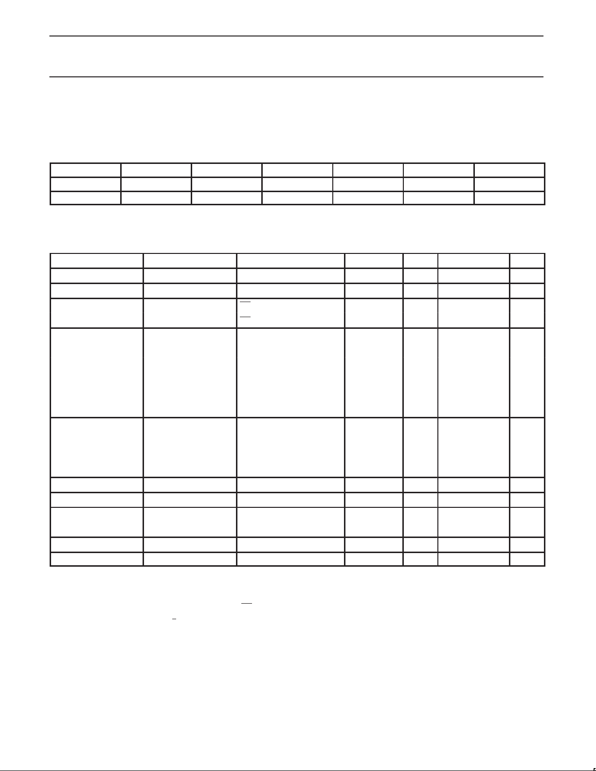
dependent on the output capacitance loading of the device. At a
minimum, a 0.1uF ceramic capacitor (high frequency, low inherent
inductance) should be used on each device between V
and between V
CC
CC
2.4 VCC+0.3V V
89C535/89C536/89C538
and GND to minimize transient effects.
PP
14 PF VI
16 pF V
10 µA
10 µA
1 mA
(Note 6)
=12V.
PP
and GND,
CC
= 0V
N
= 0V
OUT
1997 Jun 05
26
Page 27
Philips Semiconductors Preliminary specification
CMOS single-chip 8-bit microcontrollers
with FLASH program memory
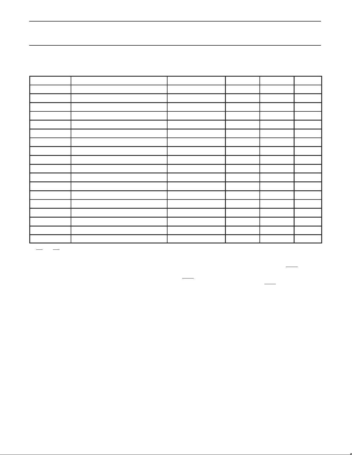
AC CHARACTERISTICS
T
= 0°C to 70°C, VCC = 5V 10%, VPP = 12V 5%
amb
SYMBOL
τ
VPS
τ
OES
τ
CWC
τ
CEP
τ
EPH1
τ
CEPH2
τ
AS
τ
AH1
τ
DS
τ
DH
τ
CESP
τ
CES
τ
CESC
τ
VPH
τ
DF
τ
DPA
τ
AETC
τ
AVT
NOTES:
and OE must be fixed high during VPP transition from 5V to 12V or from 12V to 5V.
1. CE
is defined as the time at which the output achieves the open circuit condition and data is no longer driven.
2. τ
DF
PARAMETER CONDITION MIN MAX UNIT
VPP setup time 100 ns
OE setup time 100 ns
Command programming cycles 150 ns
WE programming pulse width 60 ns
WE programming pulse width High 20 ns
WE programming pulse width High 100 ns
Address setup time 0 ns
Address hold time for DATA Polling 0 ns
DATA setup time 50 ns
DATA hold time 10 ns
CE setup time before DATA polling/toggle bit 100 ns
CE setup time 0 ns
CE setup time before command write 100 ns
VPP hold time 100 ns
Output disable time (Note 2) 35 ns
DATA polling/toggle bit access time 150 ns
Total erase time in auto chip erase 5(TYP) s
Total programming time in auto verify 15 300
89C535/89C536/89C538
s
Timing Waveform
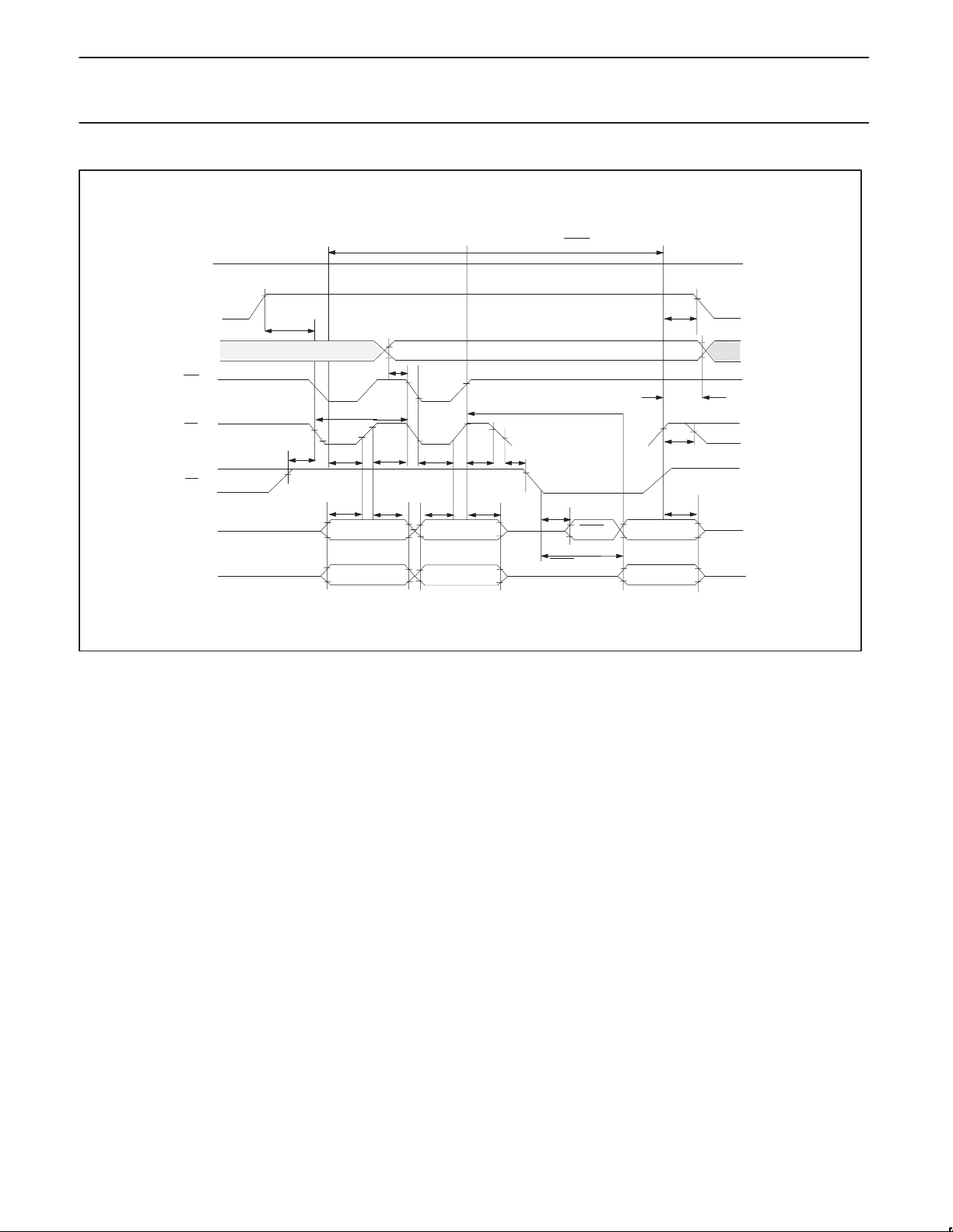
Automatic Programming
One byte of data is programmed. Verifying in fast algorithm and
additional programming by external control are not required because
these operations are executed automatically by an internal control
circuit. Programming completion can be verified by DATA
polling and
toggle bit checking after automatic verify starts. Device outputs
DATA
during programming and DATA after programming on Q7. Q0
to Q5(Q6 is for toggle bit; see toggle bit, DATA
polling, timing
waveform) are in high impedance.
1997 Jun 05
27
Page 28
Philips Semiconductors Preliminary specification
CMOS single-chip 8-bit microcontrollers
with FLASH program memory
SETUP AUTO PROGRAM/
PROGRAM COMMAND
V
5V
CC
12V
V
PP
OV
A0–A15
WE
CE
OE
Q7
τ
QES
τ
VPS
τ
AS
τcwc
τ
τ
CEP
τ
DS
COMMAND IN
CEPH1
τ
DH
τ
CEP
τ
DS
DATA IN
AUTO PROGRAM & DATA
ADDRESS
VALID
τ
AVT
τ
CESPτCES
τ
DH
τ
DPA
89C535/89C536/89C538
POLLING
τ
VPH
τ
AH1
τ
CESC
t
DF
DATA
DATA
Q0–Q5
COMMAND IN
COMMAD #40H
Figure 22. Automatic Programming Timing Waveform
A
UTOMATIC CHIP ERASE
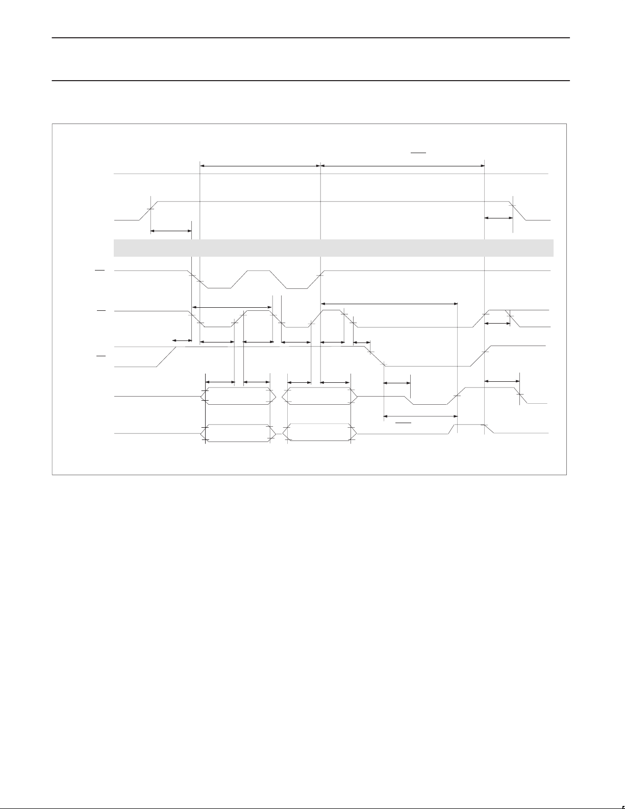
All data in the FLASH memory is erased. External erase verification
is not required. Erasure completion can be verified by DATA polling
and toggle bit checking after automatic erase starts. Device outputs
DATA IN
DATA
POLLING
DATA
su00877
0 during erasure and 1 after erasure on Q7, Q0 to Q5 (Q6 is for
toggle bit; see toggle bit, DATA polling, timing waveform) are in high
impedance.
1997 Jun 05
28
Page 29
Philips Semiconductors Preliminary specification
CMOS single-chip 8-bit microcontrollers
with FLASH program memory
RESET
SETUP AUTO CHIP ERASE/
ERASE COMMAND
V
5V
CC
12V
V
PP
OV
A0–A15
WE
CE
τ
VPS
τ
CWC
τ
τ
QES
CEP
τ
CEPH1
89C535/89C536/89C538
AUTO CHIP ERASE & DATA
τ
AETC
τ
CEP
τ
CESP
τCES
POLLING
τ
VPH
τ
CESC
Q0–Q5
OE
Q7
τ
DS
COMMAND IN
COMMAND IN
τ
DH
τ
DS
COMMAND IN
COMMAND IN
τ
DH
τ
DPA
DATA POLLING
Figure 23. Automatic Chip Erase Timing Waveform
τ
DF
su00878
1997 Jun 05
29
Page 30
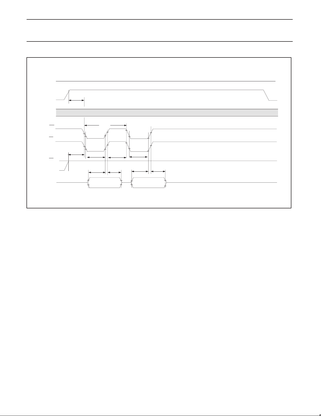
Philips Semiconductors Preliminary specification
CMOS single-chip 8-bit microcontrollers
with FLASH program memory
V
CC
5V
12V
V
PP
0V
A0–A15
WE
CE
OE
τ
VPS
t
CWC
τ
QES
τ
CEP
τ
τ
CEPH1
τ
DS
DH
τ
CEP
τ
τ
DS
DH
89C535/89C536/89C538
Q0–Q7
COMMAND IN
FFH
COMMAND IN
Figure 24. Reset Timing Waveform
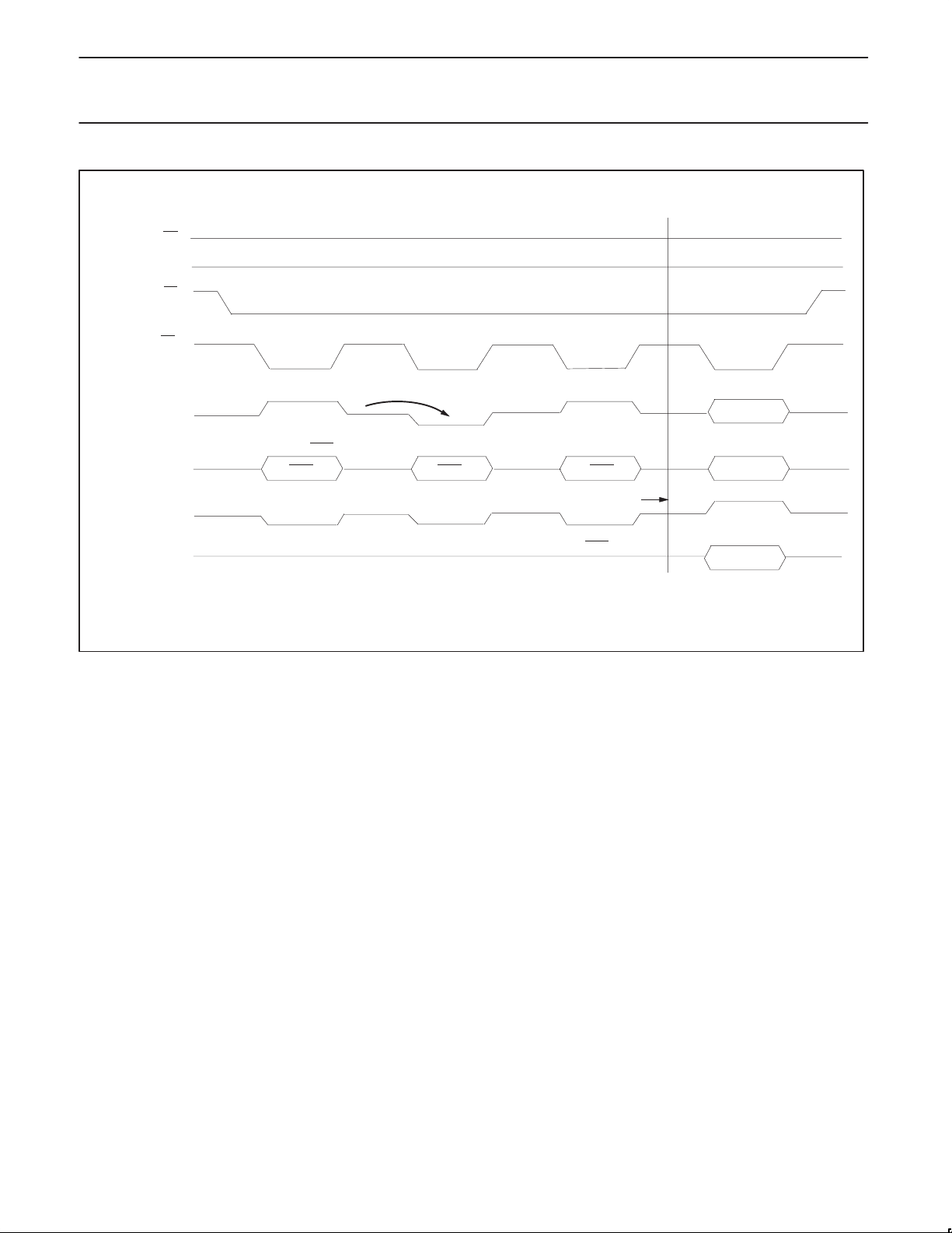
Toggle Bit, Data Polling
Toggle bit appears in Q6, when program/erase is operating. DATA
polling appears in Q7 during programming or erase.
FFH
su00879
1997 Jun 05
30
Page 31
Philips Semiconductors Preliminary specification
CMOS single-chip 8-bit microcontrollers
with FLASH program memory
HIGH
WE
12V
V
PP
CE
OE
OE
DURING P/E
O7
DURING P
O7
DURING P
O0–O5
HIGH–Z
HIGH–Z
HIGH–Z
HIGH–Z
DATA
DATA
POLLING
TOGGLE BIT
DATA DATA DATA
89C535/89C536/89C538
DATA
PROGRAM/ERASE COMPLETE
DATA POLLING
DATA
Figure 25. Toggle Bit, Data Polling Timing Waveform
su00880
1997 Jun 05
31
Page 32
Philips Semiconductors Preliminary specification
CMOS single-chip 8-bit microcontrollers
with FLASH program memory
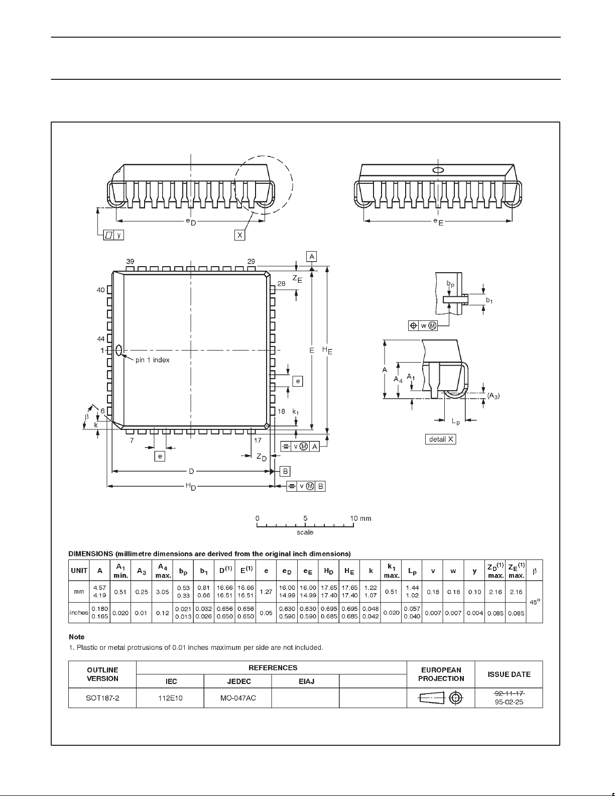
PLCC44: plastic leaded chip carrier; 44 leads SOT187-2
89C535/89C536/89C538
1997 June 05
32
Page 33
Philips Semiconductors Preliminary specification
CMOS single-chip 8-bit microcontrollers
with FLASH program memory
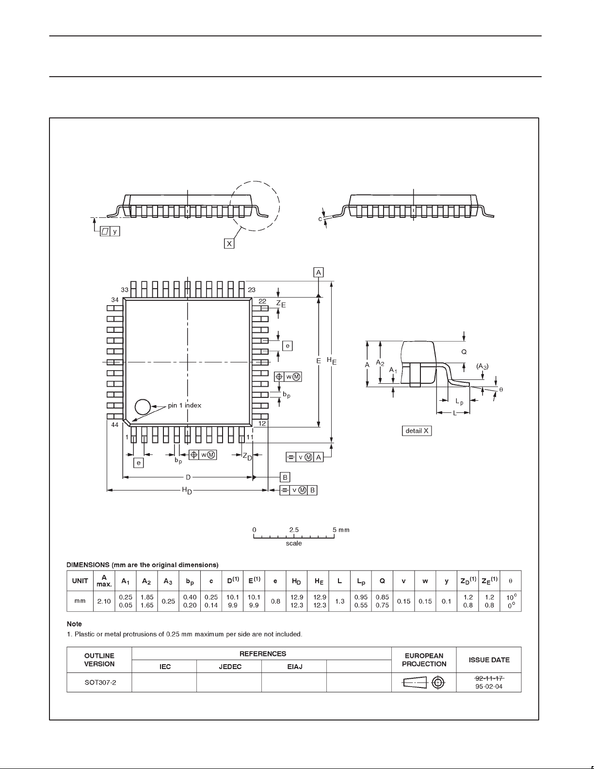
QFP44: plastic quad flat package; 44 leads (lead length 1.3 mm); body 10 x 10 x 1.75 mm SOT307-2
89C535/89C536/89C538
1997 June 05
33
Page 34

Philips Semiconductors Preliminary specification
CMOS single-chip 8-bit microcontrollers
with FLASH program memory
NOTES
89C535/89C536/89C538
1997 June 05
34
Page 35

Philips Semiconductors Preliminary specification
CMOS single-chip 8-bit microcontrollers
with FLASH program memory
DEFINITIONS
89C535/89C536/89C538
Data Sheet Identification Product Status Definition
Objective Specification
Preliminary Specification
Product Specification
Philips Semiconductors and Philips Electronics North America Corporation reserve the right to make changes, without notice, in the products,
including circuits, standard cells, and/or software, described or contained herein in order to improve design and/or performance. Philips
Semiconductors assumes no responsibility or liability for the use of any of these products, conveys no license or title under any patent, copyright,
or mask work right to these products, and makes no representations or warranties that these products are free from patent, copyright, or mask
work right infringement, unless otherwise specified. Applications that are described herein for any of these products are for illustrative purposes
only. Philips Semiconductors makes no representation or warranty that such applications will be suitable for the specified use without further testing
or modification.
LIFE SUPPORT APPLICA TIONS
Philips Semiconductors and Philips Electronics North America Corporation Products are not designed for use in life support appliances, devices,
or systems where malfunction of a Philips Semiconductors and Philips Electronics North America Corporation Product can reasonably be expected
to result in a personal injury. Philips Semiconductors and Philips Electronics North America Corporation customers using or selling Philips
Semiconductors and Philips Electronics North America Corporation Products for use in such applications do so at their own risk and agree to fully
indemnify Philips Semiconductors and Philips Electronics North America Corporation for any damages resulting from such improper use or sale.
Philips Semiconductors
811 East Arques Avenue
P.O. Box 3409
Sunnyvale, California 94088–3409
Telephone 800-234-7381
Formative or in Design
Preproduction Product
Full Production
This data sheet contains the design target or goal specifications for product development. Specifications
may change in any manner without notice.
This data sheet contains preliminary data, and supplementary data will be published at a later date. Philips
Semiconductors reserves the right to make changes at any time without notice in order to improve design
and supply the best possible product.
This data sheet contains Final Specifications. Philips Semiconductors reserves the right to make changes
at any time without notice, in order to improve design and supply the best possible product.
Copyright Philips Electronics North America Corporation 1997
All rights reserved. Printed in U.S.A.
1997 June 05
35
 Loading...