

Page 1

INTEGRATED CIRCUITS
80C575/83C575/87C575
80C51 8-bit microcontroller family
8K/256 OTP/ROM/ROMless, 4 comparator,
failure detect circuitry, watchdog timer
Product specification
Supersedes data of 1998 Jan 27
IC20 Data Handbook
1998 May 01
Page 2
Philips Semiconductors Product specification
80C51 8-bit microcontroller family
8K/256 OTP/ROM/ROMless, 4 comparator, failure detect circuitry, watchdog timer
DESCRIPTION
The Philips 80C575/83C575/87C575 is a
high-performance microcontroller fabricated
with Philips high-density CMOS technology.
The Philips CMOS technology combines the
high speed and density characteristics of
HMOS with the low power attributes of
CMOS. Philips epitaxial substrate minimizes
latch-up sensitivity.
The 8XC575 contains an 8k × 8 ROM
(83C575) EPROM (87C575), a 256 × 8 RAM,
32 I/O lines, three 16-bit counter/timers, a
Programmable Counter Array (PCA), a
seven-source, two-priority level nested
interrupt structure, an enhanced UART, four
analog comparators, power-fail detect and
oscillator fail detect circuits, and on-chip
oscillator and clock circuits.
In addition, the 8XC575 has a low active
reset, and the port pins are reset to a low
level. There is also a fully configurable
watchdog timer, and internal power on clear
circuit. The part includes idle mode and
power-down mode states for reduced power
consumption.
FEA TURES
•80C51 based architecture
– 8k × 8 ROM (83C575)
– 8k × 8 EPROM (87C575)
– ROMless (80C575)
– 256 × 8 RAM
– Three 16-bit counter/timers
– Programmable Counter Array
– Enhanced UART
– Boolean processor
– Oscillator fail detect
– Low active reset
– Asynchronous low port reset
– Schmitt trigger inputs
– 4 analog comparators
– Watchdog timer
– Low V
CC
detect
•Memory addressing capability
– 64k ROM and 64k RAM
•Power control modes:
– Idle mode
– Power-down mode
•CMOS and TTL compatible
•4.0 to 16MHz
•Extended temperature ranges
•OTP package available
80C575/83C575/
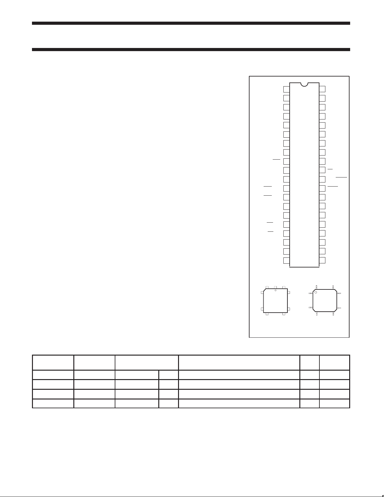
PIN CONFIGURATIONS
CMP0+/P1.0/T2
CMP0-/P1.1/T2EX
ECI/P1.2
CMP0/CEX0/P1.3
CMP1/CEX1/P1.4
CMP2/CEX2/P1.5
CMP3/CEX3/P1.6
CEX4/P1.7
RxD/P3.0
TxD/P3.1
INT0
INT1/P3.3
CMPR-/T0/P3.4
CMP1+/T1/P3.5
CMP2+/WR
CMP3+/RD/P3.7
7
17
18 28
1
2
3
4
5
6
7
8
RST
9
10
11
12
/P3.2
13
14
15
/P3.6
16
17
XTAL2
18
XTAL1
19
20
V
SS
644140
LCC
DUAL
IN-LINE
PACKAGE
39
29
1
11
87C575
40
V
DD
39
P0.0/AD0
38
P0.1/AD1
37
P0.2/AD2
36
P0.3/AD3
35
P0.4/AD4
34
P0.5/AD5
33
P0.6/AD6
32
P0.7/AD7
31
EA/V
PP
30
ALE/PROG
29
PSEN
28
P2.7/A15
27
P2.6/A14
26
P2.5/A13
25
P2.4/A12
24
P2.3/A11
23
P2.2/A10
22
P2.1/A9
21
P2.0/A8
34
PQFP
12
22
33
23
SU00234
ORDERING INFORMA TION
ROMless ROM EPROM
1
TEMPERATURE RANGE °C AND PACKAGE
FREQ
(MHz)
P80C575EBPN P83C575EBPN P87C575EBPN OTP 0 to +70, 40-Pin Plastic Dual In-line Package 16 SOT129-1
P80C575EBAA P83C575EBAA P87C575EBAA OTP 0 to +70, 44-Pin Plastic Leaded Chip Carrier 16 SOT187-2
P80C575EHAA P83C575EHAA P87C575EHAA OTP –40 to +125, 44-Pin Plastic Leaded Chip Carrier 16 SOT187-2
P80C575EBBB P83C575EBBB P87C575EBBB OTP 0 to +70, 44-Pin Plastic Quad Flat Pack 16 SOT307-2
NOTE:
1. OTP - One Time Programmable EPROM.
1998 May 01 853-1684 19332
2
DRAWING
NUMBER
Page 3
Philips Semiconductors Product specification
80C51 8-bit microcontroller family
8K/256 OTP/ROM/ROMless, 4 comparator, failure detect circuitry, watchdog timer
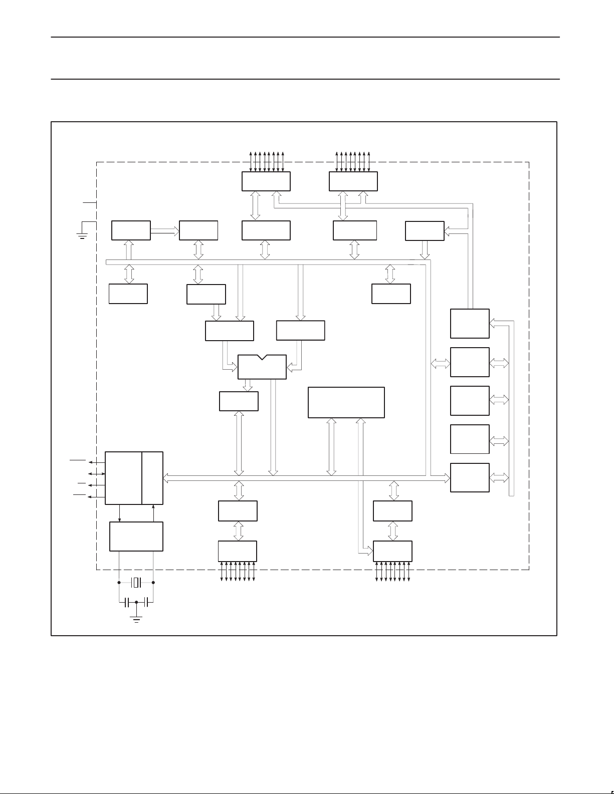
BLOCK DIAGRAM
P0.0-P0.7 P2.0-P2.7
PORT 0
DRIVERS
V
CC
V
SS
RAM ADDR
REGISTER
B
REGISTER
RAM
ACC
TMP2
PORT 0
LATCH
TMP1
PORT 2
DRIVERS
PORT 2
LATCH
STACK
POINTER
ROM/
EPROM
80C575/83C575/
87C575
PROGRAM
ADDRESS
REGISTER
PSEN
ALE
EA
RST
TIMING
AND
CONTROL
OSCILLATOR
XTAL1 XTAL2
INSTRUCTION
PD
REGISTER
PSW
PORT 1
LATCH
PORT 1
DRIVERS
P1.0-P1.7
ALU
SFRs
TIMERS
PCA
PORT 3
LATCH
PORT 3
DRIVERS
P3.0-P3.7
BUFFER
PC
INCRE-
MENTER
PROGRAM
COUNTER
DPTR
SU00238
1998 May 01
3
Page 4
Philips Semiconductors Product specification
80C51 8-bit microcontroller family
8K/256 OTP/ROM/ROMless, 4 comparator, failure detect circuitry, watchdog timer
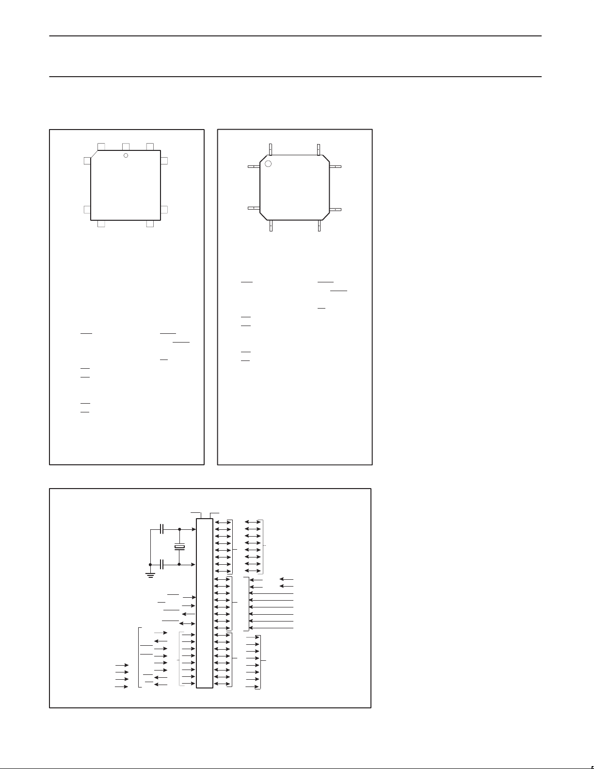
CERAMIC AND PLASTIC LEADED CHIP CARRIER PIN FUNCTIONS
6140
7
LCC
17
18 28
Pin Function
1 NC*
2 T2/P1.0/CMP0+
3 T2EX/P1.1/CMP0–
4 P1.2/ECI
5 P1.3/CMP0/CEX0
6 P1.4/CMP1/CEX1
7 P1.5/CMP2/CEX2
8 P1.6/CMP3/CEX3
9 P1.7/CEX4
10 RST
11 RxD/P3.0
12 NC*
13 TxD/P3.1
14 INT
0/P3.2
1/P3.3
15 INT
16 T0/P3.4/CMPR–
17 T1/P3.5/CMP1+
/P3.6/CMP2+
18 WR
19 RD
/P3.7/CMP3+
20 XTAL2
21 XTAL1
22 V
SS
* NO INTERNAL CONNECTION
39
29
Pin Function
23 NC*
24 P2.0/A8
25 P2.1/A9
26 P2.2/A10
27 P2.3/A11
28 P2.4/A12
29 P2.5/A13
30 P2.6/A14
31 P2.7/A15
32 PSEN
33 ALE/PROG
34 NC*
/V
35 EA
PP
36 P0.7/AD7
37 P0.6/AD6
38 P0.5/AD5
39 P0.4/AD4
40 P0.3/AD3
41 P0.2/AD2
42 P0.1/AD1
43 P0.0/AD0
44 V
CC
SU00235
PLASTIC QUAD FLAT PACK PIN FUNCTIONS
44 34
1
PQFP
11
12 22
Pin Function
1 P1.5/CMP2/CEX2
2 P1.6/CMP3/CEX3
3 P1.7/CEX4
4 RST
5 RxD/P3.0
6 NC*
7 TxD/P3.1
0/P3.2
8 INT
9 INT
1/P3.3
10 T0/P3.4/CMPR–
11 T1/P3.5/CMP1+
/P3.6/CMP2+
12 WR
/P3.7CMP3+
13 RD
14 XTAL2
15 XTAL1
16 V
SS
17 NC*
18 P2.0/A8
19 P2.1/A9
20 P2.2/A10
21 P2.3/A11
22 P2.4/A12
* NO INTERNAL CONNECTION
Pin Function
23 P2.5/A13
24 P2.6/A14
25 P2.7/A15
26 PSEN
27 ALE/PROG
28 NC*
29 EA
/V
PP
30 P0.7/AD7
31 P0.6/AD6
32 P0.5/AD5
33 P0.4/AD4
34 P0.3/AD3
35 P0.2/AD2
36 P0.1/AD1
37 P0.0/AD0
38 V
CC
39 NC*
40 T2/P1.0/CMP0+
41 T2EX/P1.1/CMP0–
42 P1.2/ECI
43 P1.3/CMP0/CEX0
44 P1.4/CMP1/CEX1
33
23
SU00236
80C575/83C575/
87C575
LOGIC SYMBOL
CMPR–
CMP1+
CMP2+
CMP3+
1998 May 01
EA/V
PSEN
ALE/PROG
RxD
TxD
INT0
INT1
T0
T1
WR
RD
SECONDARY FUNCTIONS
XTAL1
XTAL2
RST
PP
PORT 3
V
V
SS
CC
ADDRESS AND
PORT 1PORT 2
DATA BUS
T2
T2EX
ADDRESS BUS
CMP0+
CMP0–
ECI
CMP0/CEX0
CMP1/CEX1
CMP2/CEX2
CMP3/CEX3
CEX4
SU00237
PORT 0
4
Page 5

Philips Semiconductors Product specification
80C51 8-bit microcontroller family
8K/256 OTP/ROM/ROMless, 4 comparator, failure detect circuitry, watchdog timer
80C575/83C575/
87C575
PIN DESCRIPTIONS
PIN NUMBER
MNEMONIC DIP LCC QFP TYPE NAME AND FUNCTION
V
SS
V
CC
P0.0-0.7 39-32 43-36 37-30 I/O Port 0: Port 0 is an open-drain bidirectional I/O port. Port 0 pins that have 1s written to them
P1.0-P1.7 1-8 2-9 40-44
P2.0-P2.7 21-28 24-31 18-25 I/O Port 2: Port 2 is an 8-bit bidirectional I/O port with internal pull-ups. Port 2 pins that have 1s
P3.0-P3.7 10-17 11,
20 22 16 I Ground: 0V reference.
40 44 38 I Power Supply: This is the power supply voltage for normal, idle, and power-down
1-3
1 2 40 I/O P1.0 T2 Timer 2 external I/O – clockout (programmable)
2 3 41 I P1.1 T2EX Timer 2 capture input
3 4 42 I P1.2 ECI PCA count input
4 5 43 I/O P1.3 CEX0 PCA module 0 external I/O
5 6 44 I/O P1.4 CEX1 PCA module 1 external I/O
6 7 1 I/O P1.5 CEX2 PCA module 2 external I/O
7 8 2 I/O P1.6 CEX3 PCA module 3 external I/O
8 9 3 I/O P1.7 CEX4 PCA module 4 external I/O
13-195,7-13
operation.
float and can be used as high-impedance inputs. Port 0 is also the multiplexed low-order
address and data bus during accesses to external program and data memory. In this
application, it uses strong internal pull-ups when emitting 1s. Port 0 also receives code
bytes during EPROM programming and outputs code bytes during program verification.
External pull-ups are required during program verification. During reset, port 0 will be
asynchronously driven low and will remain low until written to by software. All port 0 pins
have Schmitt trigger inputs with 200mV hysteresis. A weak pulldown on port 0 guarantees
positive leakage current (see DC Electrical Characteristics: I
I/O Port 1: Port 1 is an 8-bit bidirectional I/O port. Port 1 pins have internal pull-ups such that
pins that have 1s written to them can be used as inputs but will source current when
externally pulled low (see DC Electrical Characteristics: I
address byte during program memory verification and EPROM programming. During reset,
port 1 will be asynchronously driven low and will remain low until written to by software. All
port 1 pins have Schmitt trigger inputs with 50mV hysteresis. Port 1 pins also serve
alternate functions as follows:
CMP0+ Comparator 0 positive input
CMP0- Comparator 0 negative input
CMP0 Comparator 0 output
CMP1 Comparator 1 output
CMP2 Comparator 2 output
CMP3 Comparator 3 output
written to them can be used as inputs, but will source current when externally pulled low
(see DC Electrical Characteristics: I
accesses to external program and data memory that use 16-bit addresses (MOVX
@DPTR). In this application, it uses strong internal pull-ups when emitting 1s. Port 2
receives the high-order address byte during program verification and EPROM programming.
During reset, port 2 will be asynchronously driven low and will remain low until written to by
software. Port 2 can be made open drain by writing to the P2OD register (AIH). In open
drain mode, weak pulldowns on port 2 guarantee positive leakage current (see DC
Electrical Characteristics I
I/O Port 3: Port 3 is an 8-bit bidirectional I/O port with internal pull-ups. Port 3 pins except P3.1
that have 1s written to them can be used as inputs but will source current when externally
pulled low (see DC Electrical Characteristics: I
while transmitting serial data, in which case the strong pull-up will remain on continuously
when outputting a 1 level. The P3.1 output drive level when transmitting can be set to one of
two levels by the writing to the P3.1 register bit. During reset all pins (except P3.1) will be
asynchronously driven low and will remain low until written to by software. All port 3 pins
have Schmitt trigger inputs with 200mV hysteresis, except P3.2 and P3.3, which have 50mV
hysteresis. Port 3 pins serve alternate functions as follows:
).
L1
). Port 2 emits the high-order address byte during
IL
). P3.1 will be a high impedance pin except
IL
).
L1
). Port 1 receives the low-order
IL
1998 May 01
5
Page 6

Philips Semiconductors Product specification
80C51 8-bit microcontroller family
8K/256 OTP/ROM/ROMless, 4 comparator, failure detect circuitry, watchdog timer
80C575/83C575/
87C575
PIN DESCRIPTIONS (Continued)
PIN NUMBER
MNEMONIC DIP LCC QFP TYPE NAME AND FUNCTION
Port 3: (continued)
10 11 5 I P3.0 RxD Serial receive port
11 13 7 O P3.1 TxD Serial transmit port enabled only when transmitting serial data
12 14 8 I P3.2 INT0 External interrupt 0
13 15 9 I P3.3 INT1 External interrupt 1
14 16 10 I P3.4 T0 Timer/counter 0 input
15 17 11 I P3.5 T1 Timer/counter 1 input
16 18 12 O P3.6 WR External data memory write strobe
17 19 13 O P3.7 RD External data memory read strobe
RST 9 10 4 I Reset: A low on this pin asynchronously resets all port pins to a low state except P3.1. The
ALE/PROG 30 33 27 I/O Address Latch Enable/Program Pulse: Output pulse for latching the low byte of the
PSEN 29 32 26 O Program Store Enable: The read strobe to external program memory. When the device is
EA/V
PP
XTAL1 19 21 15 I Crystal 1: Input to the inverting oscillator amplifier and input to the internal clock generator
XTAL2 18 20 14 O Crystal 2: Output from the inverting oscillator amplifier.
31 35 29 I External Access Enable/Programming Supply Voltage: EA must be externally held low
CMPR- Common - reference to comparators 1, 2, 3
CMP1+ Comparator 1 positive input
CMP2+ Comparator 2 positive input
CMP3+ Comparator 3 positive input
pin must be held low with the oscillator running for 24 oscillator cycles to initialize the
internal registers. An internal diffused resistor to V
an external capacitor to V
noise immunity with a slow rising input voltage.
address during an access to external memory. In normal operation, ALE is emitted at a
constant rate of 1/6 the oscillator frequency, and can be used for external timing or clocking.
Note that one ALE pulse is skipped during each access to external data memory. ALE is
switched off if the bit 0 in the AUXR register (8EH) is set. This pin is also the program pulse
input (PROG
executing code from the external program memory, PSEN is activated twice each machine
cycle, except that two PSEN
memory. PSEN
to enable the device to fetch code from external program memory locations 0000H to
1FFFH. If EA
program counter contains an address greater than 1FFFH. This pin also receives the
12.75V programming supply voltage (V
circuits.
) during EPROM programming.
is not activated during fetches from internal program memory.
is held high, the device executes from internal program memory unless the
. RST has a Schmitt trigger input stage to provide additional
SS
activations are skipped during each access to external data
) during EPROM programming.
PP
permits a power on reset using only
CC
1998 May 01
6
Page 7
Philips Semiconductors Product specification
80C51 8-bit microcontroller family
8K/256 OTP/ROM/ROMless, 4 comparator, failure detect circuitry, watchdog timer
80C575/83C575/
87C575
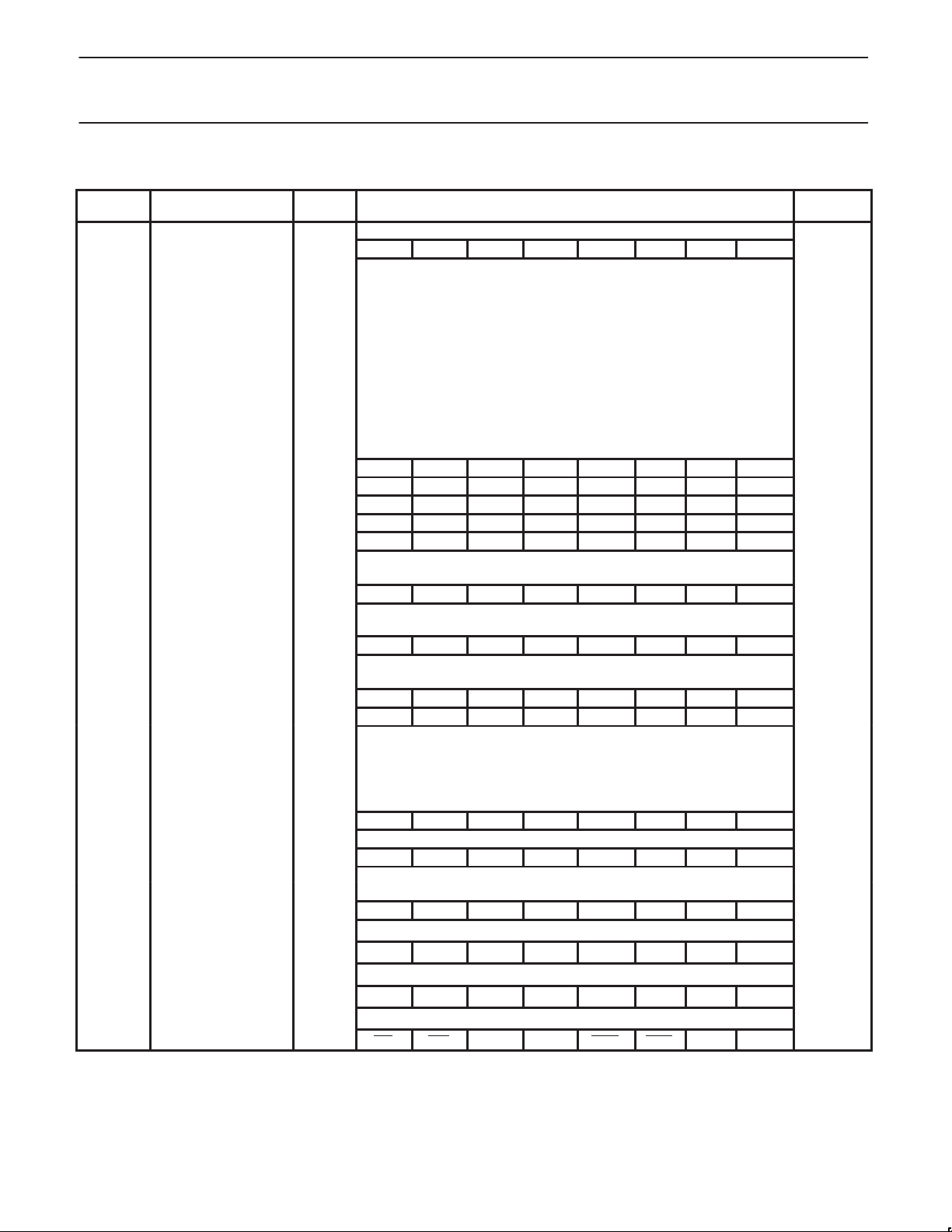
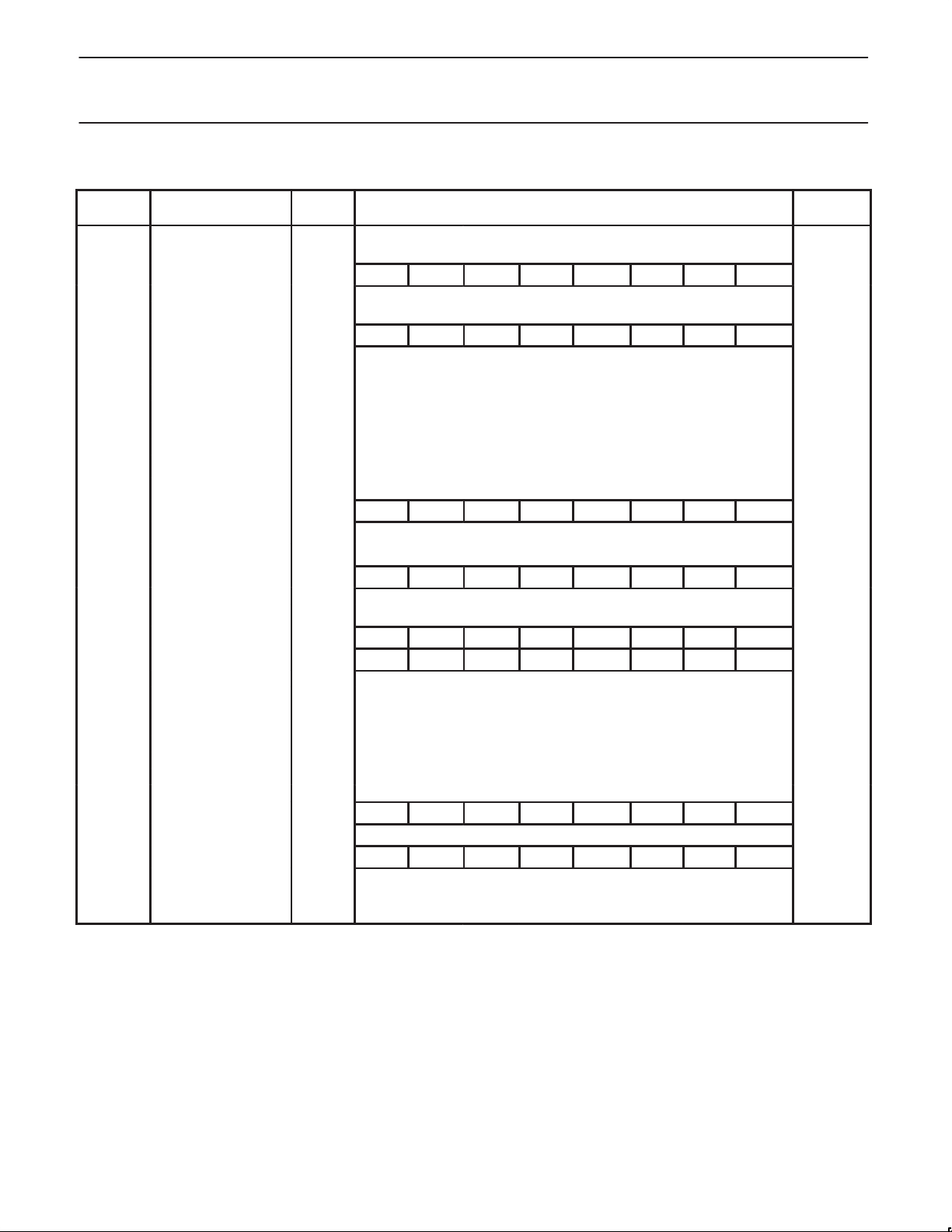
Table 1. 87C575 Special Function Registers
SYMBOL DESCRIPTION
ACC* Accumulator E0H E7 E6 E5 E4 E3 E2 E1 E0 00H
AUXR# Auxiliary 8EH – – – – – – LO AO xxxxxx00B
B* B register F0H F7 F6 F5 F4 F3 F2 F1 F0 00H
CCAP0H# Module 0 Capture High FAH xxxxxxxxB
CCAP1H# Module 1 Capture High FBH xxxxxxxxB
CCAP2H# Module 2 Capture High FCH xxxxxxxxB
CCAP3H# Module 3 Capture High FDH xxxxxxxxB
CCAP4H# Module 4 Capture High FEH xxxxxxxxB
CCAP0L# Module 0 Capture Low EAH xxxxxxxxB
CCAP1L# Module 1 Capture Low EBH xxxxxxxxB
CCAP2L# Module 2 Capture Low ECH xxxxxxxxB
CCAP3L# Module 3 Capture Low EDH xxxxxxxxB
CCAP4L# Module 4 Capture Low EEH xxxxxxxxB
CCAPM0# Module 0 Mode DAH – ECOM CAPP CAPN MAT TOG PWM ECCF x0000000B
CCAPM1# Module 1 Mode DBH – ECOM CAPP CAPN MAT TOG PWM ECCF x0000000B
CCAPM2# Module 2 Mode DCH – ECOM CAPP CAPN MAT TOG PWM ECCF x0000000B
CCAPM3# Module 3 Mode DDH – ECOM CAPP CAPN MAT TOG PWM ECCF x0000000B
CCAPM4# Module 4 Mode DEH – ECOM CAPP CAPN MAT TOG PWM ECCF x0000000B
DIRECT
ADDRESS
BIT ADDRESS, SYMBOL, OR ALTERNATIVE PORT FUNCTION
MSB LSB
RESET
VALUE
DF DE DD DC DB DA D9 D8
CCON*# PCA Counter Control D8H CF CR – CCF4 CCF3 CCF2 CCF1 CCF0 00x00000B
CH# PCA Counter High F9H 00H
CL# PCA Counter Low E9H 00H
CMOD# PCA Counter Mode D9H CIDL WDTE – – – CPS1 CPS0 ECF 00xxx000B
EF EE ED EC EB EA E9 E8
CMP*# Comparator E8H EC3DP EC2DP EC1DP EC0DP C3RO C2RO C1RO C0RO 00H
CMPE# Comparator Enable 91H
DPTR: Data Pointer (2 bytes)
DPH Data Pointer High 83H 00H
DPL Data Pointer Low 82H 00H
IE* Interrupt Enable A8H EA EC ET2 ES ET1 EX1 ET0 EX0 00H
IP* Interrupt Priority B8H – PPC PT2 PS PT1 PX1 PT0 PX0 x0000000B
P0* Port 0 80H AD7 AD6 AD5 AD4 AD3 AD2 AD1 AD0 00H
P1* Port 1 90H CEX4 CEX3 CEX2 CEX1 CEX0 EXI T2EX T2 00H
P2* Port 2 A0H AD15 AD14 AD13 AD12 AD11 AD10 AD9 AD8 00H
P3* Port 3 B0H RD WR T1 T0 INT1 INT0 TxD RxD 00H
* SFRs are bit addressable.
# SFRs are modified from or added to the 80C51 SFRs.
1. 87C575 only.
EC3TDC EC2TDC EC1TDC EC0TDC EC3OD EC2OD EC1OD EC0OD
AF AE AD AC AB AA A9 A8
BF BE BD BC BB BA B9 B8
87 86 85 84 83 82 81 80
97 96 95 94 93 92 91 90
A7 A6 A5 A4 A3 A2 A1 A0
B7 B6 B5 B4 B3 B2 B1 B0
00H
1998 May 01
7
Page 8
Philips Semiconductors Product specification
80C51 8-bit microcontroller family
8K/256 OTP/ROM/ROMless, 4 comparator, failure detect circuitry, watchdog timer
80C575/83C575/
87C575
Table 1. 87C575 Special Function Registers (Continued)
SYMBOL DESCRIPTION
P2OD# Port 2 Pullup Disable A1H 00H
PCON# Power Control 87H
PSW* Program Status Word D0H CY AC F0 RS1 RS0 OV – P 00H
RACAP2H#
RACAP2L
SADDR# Slave Address A9H 00H
SADEN# Slave Address Mask B9H 00H
SBUF Serial Data Buffer 99H xxxxxxxxB
SCON* Serial Control 98H SM0 SM1 SM2 REN TB8 RB8 TI RI 00H
SP Stack Pointer 81H 07H
TCON* Timer Control 88H TF1 TR1 TF0 TR0 IE1 IT1 IE0 IT0 00H
Timer 2 Capture High CBH 00H
# Timer 2 Capture Low CAH 00H
DIRECT
ADDRESS
BIT ADDRESS, SYMBOL, OR ALTERNATIVE PORT FUNCTION
MSB LSB
SMOD1 SMOD0
D7 D6 D5 D4 D3 D2 D1 D0
9F 9E 9D 9C 9B 9A 99 98
8F 8E 8D 8C 8B 8A 89 88
OSF1POF
1
LVF
1
GF0 PD IDL 00xxx000B
RESET
VALUE
CF CE CD CC CB CA C9 C8
T2CON* Timer 2 Control C8H TF2 EXF2 RCLK TCLK EXEN2 TR2 C/T2 CP/RL2 00H
T2MOD# Timer 2 Mode Control C9H – – – – – – T2OE2DCEN xxxxxxx0B
TH0 Timer High 0 8CH 00H
TH1 Timer High 1 8DH 00H
TH2# Timer High 2 CDH 00H
TL0 Timer Low 0 8AH 00H
TL1 Timer Low 1 8BH 00H
TL2# T imer Low 2 CCH 00H
TMOD Timer Mode 89H GA TE C/T M1 M0 GA TE C/T M1 M0 00H
C7 C6 C5 C4 C3 C2 C1 C0
WDCON*#Watchdog Timer Control
WDL#
WFEED1# Watchdog Feed 1 C2H xxH
WFEED2# Watchdog Feed 2 C3H xxH
* SFRs are bit addressable.
# SFRs are modified from or added to the 80C51 SFRs.
1. Reset value depends on reset source.
2. Programmable clock-out.
Watchdog Timer Reload
C0H PRE2 PRE1 PRE0 LVRE OFRE
C1H 00H
WDRUN WDTOF WDMOD
11111101B
1998 May 01
8
Page 9
Philips Semiconductors Product specification
80C51 8-bit microcontroller family
8K/256 OTP/ROM/ROMless, 4 comparator, failure detect circuitry, watchdog timer
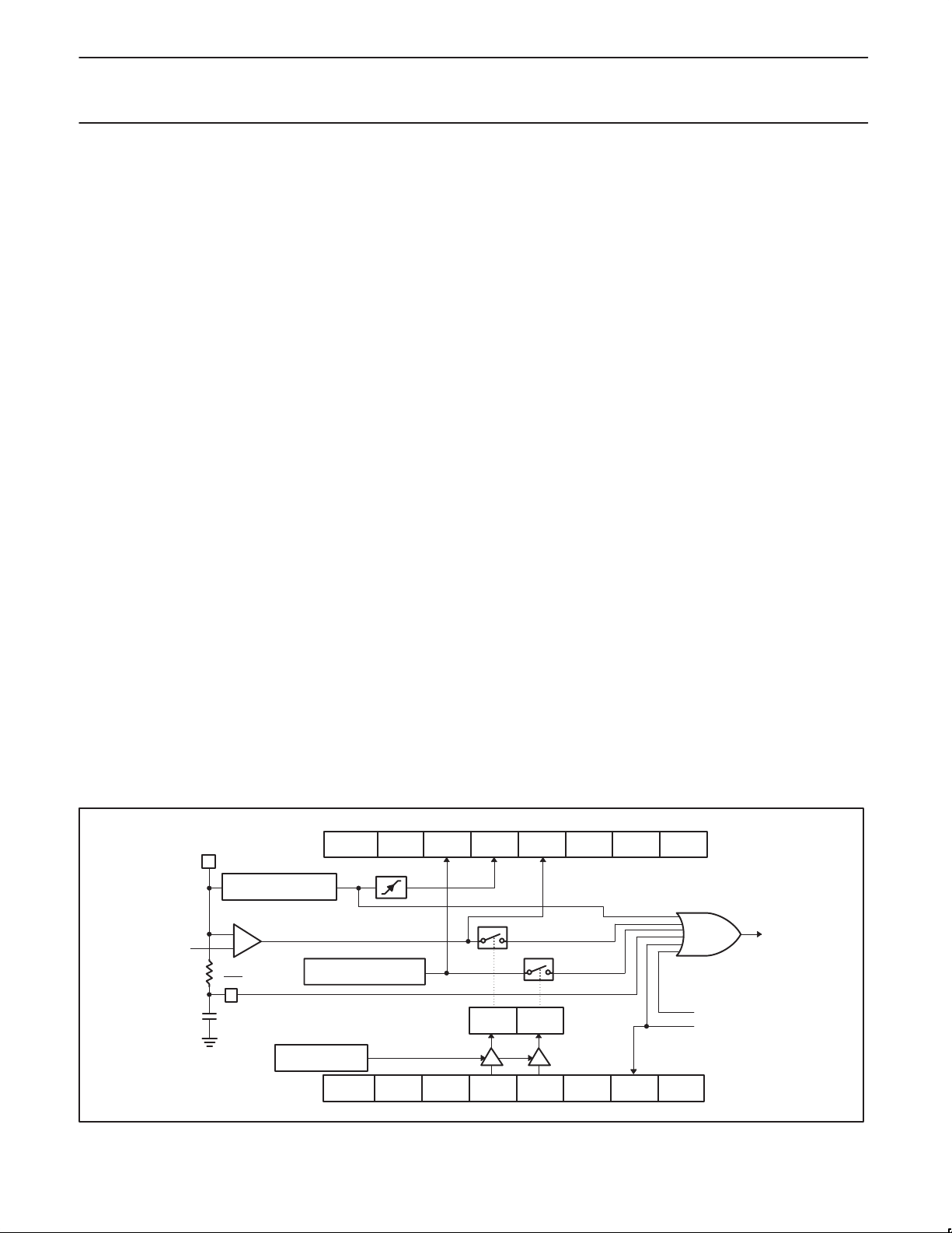
POWER ON CLEAR/ POWER ON FLAG
An on-chip Power On Detect Circuit resets
the 8XC575 and sets the Power Off Flag
(PCON.4) on power up or if V
drops to
CC
zero momentarily. The POF can only be
cleared by software. The RST pin is not
driven by the power on detect circuit. The
POF can be read by software to determine
that a power failure has occurred and can
also be set by software.
LOW VOLTAGE DETECT
An on-chip Low Voltage Detect circuit sets
the Low Voltage Flag (PCON.3) if V
below V
(see DC Electrical
LOW
Characteristics) and resets the 8XC575 if the
Low Voltage Reset Enable bit (WDCON.4) is
set. If the LVRE is cleared, the reset is
disabled but LVF will still be set if V
The RST pin is not driven by the low voltage
detect circuit. The LVF can be read by
software to determine that V
CC
LVF can be set or cleared by software.
drops
CC
is low.
CC
was low. The
OSCILLATOR FAIL DETECT
An on-chip Oscillator Fail Detect circuit sets
the Oscillator Fail Flag (PCON.5) if the
oscillator frequency drops below OSCF for
one or more cycles (see AC Electrical
Characteristics: OSCF) and resets the
8XC575 if the Oscillator Fail Reset Enable bit
(WDCON.3) is set. If OFRE is cleared, the
reset is disabled but OSF will still be set if the
oscillator fails. The RST pin is not driven by
the oscillator fail detect circuit. The OSF can
be read by software to determine that an
oscillator failure has occurred. The OSF can
be set or cleared by software.
LOW ACTIVE RESET
One of the most notable features on this part
is the low active reset. At this time this is the
only 80C51 derivative available that has low
active reset. This feature makes it easier to
interface the 8XC575 into an application to
accommodate the power-on and low voltage
conditions that can occur. The low active
reset operates exactly the same as high
active reset with the exception that the part is
put into the reset mode by applying a low
level to the reset pin. For power-on reset it is
also necessary to invert the power-on reset
circuit; connecting the 8.2K resistor from the
reset pin to V
the reset pin to ground. Figure 1 shows all of
the reset related circuitry.
When reset the port pins on the 87C575 are
driven low asynchronously . This is different
from all other 80C51 derivatives.
The 8XC575 also has Low voltage detection
circuitry that will, if enabled, force the part to
reset when V
level. Low Voltage Reset is enabled by a
normal reset. Low Voltage Reset can be
disabled by clearing LVRE (bit 4 in the
WDCON SFR) then executing a watchdog
feed sequence (A5H to WFEED1 followed
immediately by 5A to WFEED2). In addition
there is a flag (LVF) that is set if a low voltage
condition is detected. The LVF flag is set
even if the Low Voltage detection circuitry is
disabled. Notice that the Low voltage
detection circuitry does not drive the RST#
pin so the LVF flag is the only way that the
microcontroller can determine if it has been
reset due to a low voltage condition.
and the 10µf capacitor from
CC
(on the part) fails below a set
CC
80C575/83C575/
87C575
The 8XC575 has an on-chip power-on
detection circuit that sets the POF (PCON.4)
flag on power up or if the V
momentarily drops to 0V. This flag can be
used to determine if the part is being started
from a power-on (cold start) or if a reset has
occurred due to another condition (warm
start).
TIMERS
The 87C575 has four on-chip timers.
Timers 0 and 1 are identical in every way to
Timers 0 and 1 on the 80C51.
Timer 2 on the 8XC575 is identical to the
80C52 Timer 2 (described in detail in the
80C52 overview) with the exception that it is
an up or down counter. To configure the
Timer to count down the DCEN bit in the
T2MOD special function register must be set
and a low level must be present on the T2EX
pin (P1.1).
The Watchdog timer operation and
implementation is the same as that for the
8XC550 (described in the 8XC550 overview)
with the exception that the reset values of the
WDCON and WDL special function registers
have been changed. The changes in these
registers cause the watchdog timer to be
enabled with a timeout of 98304 × T
when the part is reset. The watchdog can be
disabled by executing a valid feed sequence
and then clearing WDRUN (bit 2 in the
WDCON SFR).
CC
level
OSC
(LOW V
REFERENCE)
1998 May 01
VLOW
V
CC
POWER-ON DETECT
+
CC
–
RST
WATCHDOG FEED
SMOD1 SMOD0 OSF LVF GF0 GF1 IDL
OSC FREQ BELOW OSCF
(MIN FREQUENCY)
SHADOW REGISTER
FOR WDCON
PRE2 PRE1 PRE0 LVRE OFRE WDRUN WDTOF WDMOD
POF
PCON
(87GH)
8xC575
INTERNAL
RESET
PCA WATCHDOG
WATCHDOG TIMER
WDCON
(C0H)
SU00239
Figure 1. Reset Circuitry
9
Page 10
Philips Semiconductors Product specification
80C51 8-bit microcontroller family
8K/256 OTP/ROM/ROMless, 4 comparator, failure detect circuitry, watchdog timer
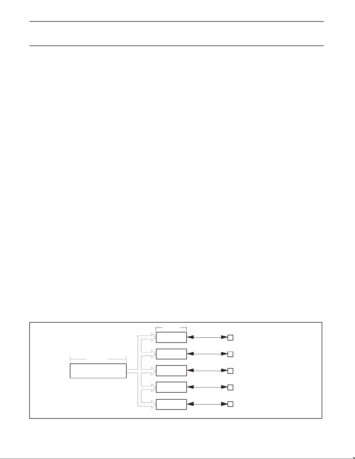
PROGRAMMABLE COUNTER ARRAY (PCA)
The Programmable Counter Array is a
special Timer that has five 16-bit
capture/compare modules associated with it.
Each of the modules can be programmed to
operate in one of four modes: rising and/or
falling edge capture, software timer,
high-speed output, or pulse width modulator.
Each module has a pin associated with it in
port 1. Module 0 is connected to P1.3(CEX0),
module 1 to P1.4(CEX1), etc.. The basic
PCA configuration is shown in Figure 2.
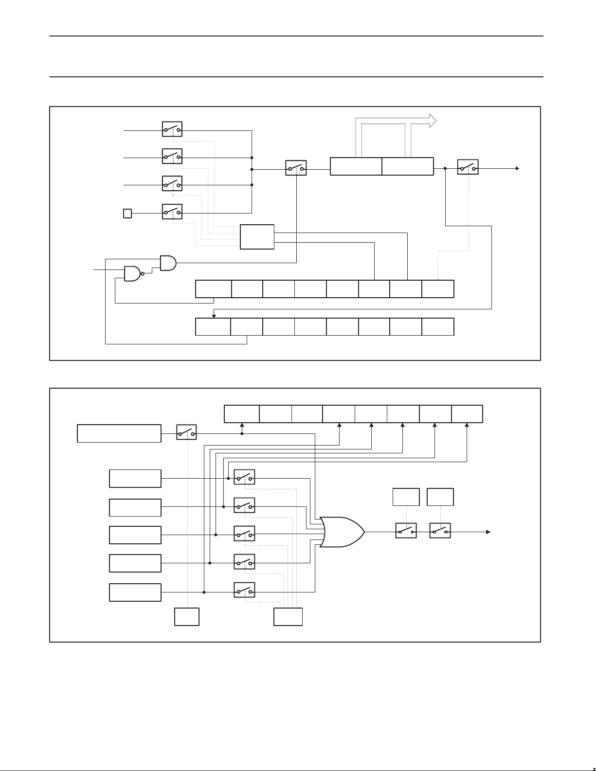
The PCA timer is a common time base for all
five modules and can be programmed to run
at: 1/12 the oscillator frequency, 1/4 the
oscillator frequency, the Timer 0 overflow , or
the input on the ECI pin (P1.2). The timer
count source is determined from the CPS1
and CPS0 bits in the CMOD SFR as follows
(see Figure 3):
CPS1 CPS0 PCA Timer Count Source
0 0 1/12 oscillator frequency
0 1 1/4 oscillator frequency
1 0 Timer 0 overflow
1 1 External Input at ECI pin
In the CMOD SFR are three additional bits
associated with the PCA. They are CIDL
which allows the PCA to stop during idle
mode, WDTE which enables or disables the
watchdog function on module 4, and ECF
which when set causes an interrupt and the
PCA overflow flag CF (in the CCON SFR) to
be set when the PCA timer overflows. These
functions are shown in Figure 3.
The watchdog timer function is implemented
in module 4 as implemented in other parts
that have a PCA that are available on the
market. However, if a watchdog timer is
required in the target application, it is
recommended to use the hardware watchdog
timer that is implemented on the 87C575
separately from the PCA (see Figure 14).
The CCON SFR contains the run control bit
for the PCA and the flags for the PCA timer
(CF) and each module (refer to Figure 6). To
run the PCA the CR bit (CCON.6) must be
set by software. The PCA is shut off by
clearing this bit. The CF bit (CCON.7) is set
when the PCA counter overflows and an
interrupt will be generated if the ECF bit in
the CMOD register is set, The CF bit can only
be cleared by software. Bits 0 through 4 of
the CCON register are the flags for the
modules (bit 0 for module 0, bit 1 for module
1, etc.) and are set by hardware when either
a match or a capture occurs. These flags
also can only be cleared by software. The
PCA interrupt system shown in Figure 4.
Each module in the PCA has a special
function register associated with it. These
registers are: CCAPM0 for module 0,
CCAPM1 for module 1, etc. (see Figure 7).
The registers contain the bits that control the
mode that each module will operate in. The
ECCF bit (CCAPMn.0 where n=0, 1, 2, 3, or
4 depending on the module) enables the CCF
flag in the CCON SFR to generate an
interrupt when a match or compare occurs in
the associated module. PWM (CCAPMn.1)
enables the pulse width modulation mode.
The TOG bit (CCAPMn.2) when set causes
the CEX output associated with the module to
toggle when there is a match between the
PCA counter and the module’s
capture/compare register . The match bit MAT
(CCAPMn.3) when set will cause the CCFn
bit in the CCON register to be set when there
is a match between the PCA counter and the
module’s capture/compare register .
The next two bits CAPN (CCAPMn.4) and
CAPP (CCAPMn.5) determine the edge that
a capture input will be active on. The CAPN
bit enables the negative edge, and the CAPP
bit enables the positive edge. If both bits are
set both edges will be enabled and a capture
will occur for either transition. The last bit in
80C575/83C575/
87C575
the register ECOM (CCAPMn.6) when set
enables the comparator function. Figure 8
shows the CCAPMn settings for the various
PCA functions.
There are two additional registers associated
with each of the PCA modules. They are
CCAPnH and CCAPnL and these are the
registers that store the 16-bit count when a
capture occurs or a compare should occur.
When a module is used in the PWM mode
these registers are used to control the duty
cycle of the output.
PCA Capture Mode
To use one of the PCA modules in the
capture mode either one or both of the
CCAPM bits CAPN and CAPP for that
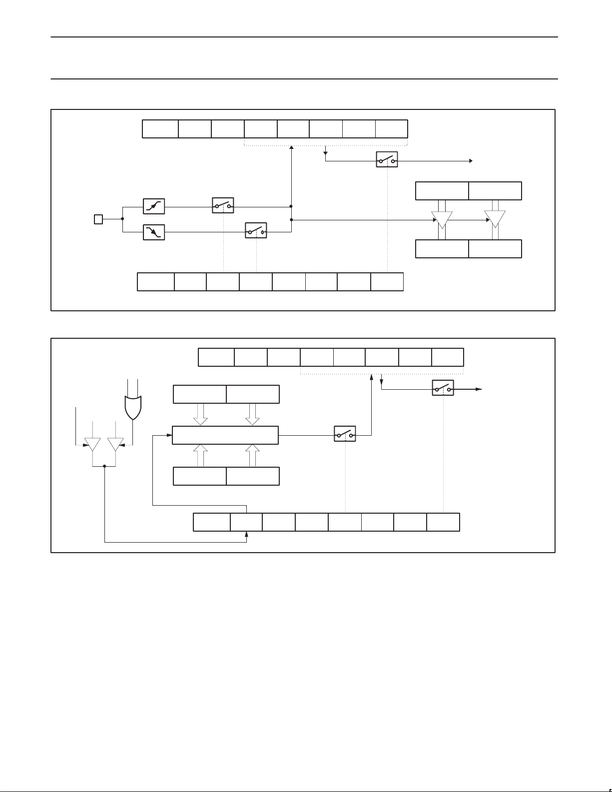
module must be set. The external CEX input
for the module (on port 1) is sampled for a
transition. When a valid transition occurs the
PCA hardware loads the value of the PCA
counter registers (CH and CL) into the
module’s capture registers (CCAPnL and
CCAPnH). If the CCFn bit for the module in
the CCON SFR and the ECCFn bit in the
CCAPMn SFR are set then an interrupt will
be generated. Refer to Figure 9.
16-bit Software Timer Mode
The PCA modules can be used as software
timers by setting both the ECOM and MAT
bits in the modules CCAPMn register. The
PCA timer will be compared to the module’s
capture registers and when a match occurs
an interrupt will occur if the CCFn (CCON
SFR) and the ECCFn (CCAPMn SFR) bits for
the module are both set (see Figure 10).
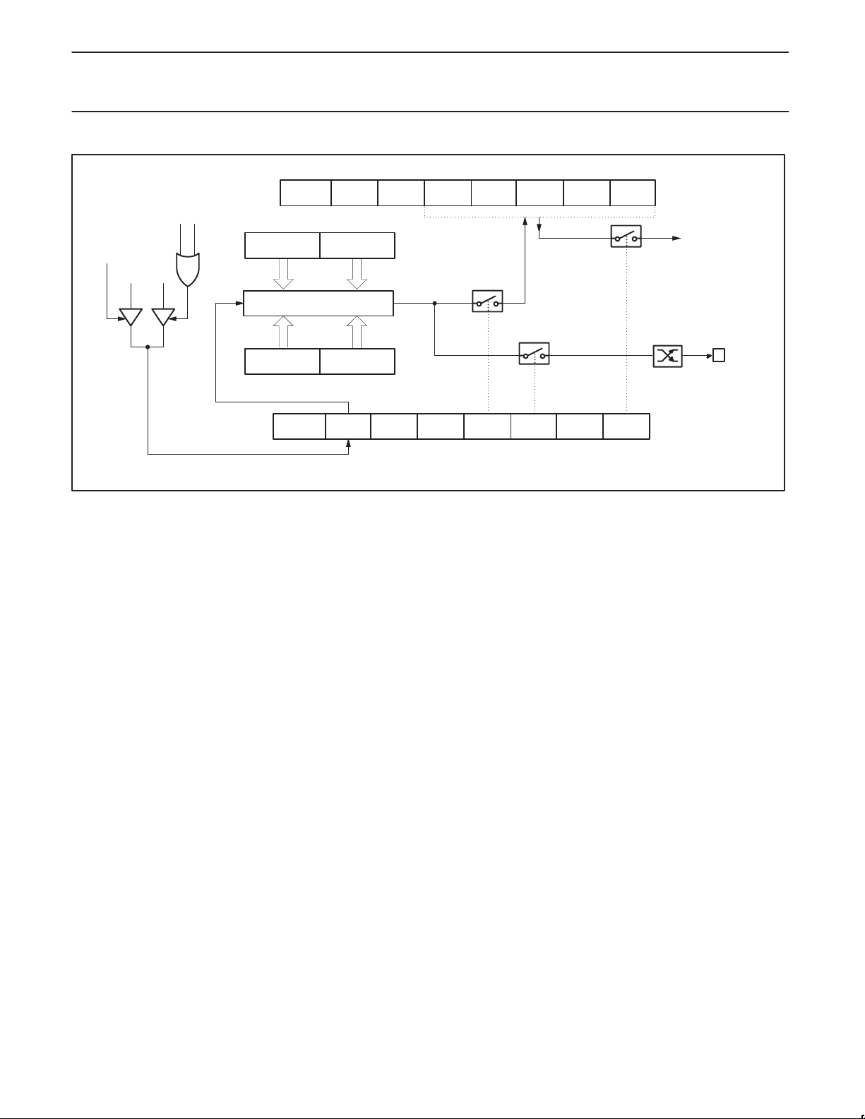
High Speed Output Mode
In this mode the CEX output (on port 1)
associated with the PCA module will toggle
each time a match occurs between the PCA
counter and the module’s capture registers.
To activate this mode the TOG, MAT, and
ECOM bits in the module’s CCAPMn SFR
must be set (see Figure 11).
MODULE FUNCTIONS:
16-BIT CAPTURE
16-BIT TIMER
16-BIT HIGH SPEED OUTPUT
8-BIT PWM
WATCHDOG TIMER (MODULE 4 ONLY)
1998 May 01
16 BITS
PCA TIMER/COUNTER
TIME BASE FOR PCA MODULES
16 BITS
MODULE 0
MODULE 1
MODULE 2
MODULE 3
MODULE 4
Figure 2. Programmable Counter Array (PCA)
10
P1.3/CEX0
P1.4/CEX1
P1.5/CEX2
P1.6/CEX3
P1.7/CEX4
SU00032
Page 11
Philips Semiconductors Product specification
80C51 8-bit microcontroller family
8K/256 OTP/ROM/ROMless, 4 comparator, failure detect circuitry, watchdog timer
OSC/12
OSC/4
TIMER 0
OVERFLOW
EXTERNAL INPUT
(P1.2/ECI)
IDLE
00
01
DECODE
10
11
CIDL WDTE –– –– –– CPS1 CPS0 ECF
CF CR CCF4 CCF3 CCF2 CCF1 CCF0––
CH CL
16–BIT UP COUNTER
80C575/83C575/
87C575
TO PCA
MODULES
OVERFLOW
CMOD
(D9H)
CCON
(D8H)
INTERRUPT
PCA TIMER/COUNTER
MODULE 0
MODULE 1
MODULE 2
MODULE 3
MODULE 4
CMOD.0 ECF
Figure 3. PCA Timer/Counter
CF CR CCF4 CCF3 CCF2 CCF1 CCF0––
CCAPMn.0 ECCFn
Figure 4. PCA Interrupt System
IE.6
EC
IE.7
EA
SU00033
CCON
(D8H)
TO
INTERRUPT
PRIORITY
DECODER
SU00034
1998 May 01
11
Page 12

Philips Semiconductors Product specification
80C51 8-bit microcontroller family
8K/256 OTP/ROM/ROMless, 4 comparator, failure detect circuitry, watchdog timer
CMOD Address = OD9H
80C575/83C575/
87C575
Reset Value = 00XX X000B
CIDL WDTE – – – CPS1 CPS0 ECF
Bit:
76543210
Symbol Function
CIDL Counter Idle control: CIDL = 0 programs the PCA Counter to continue functioning during idle Mode. CIDL = 1 programs
it to be gated off during idle.
WDTE Watchdog Timer Enable: WDTE = 0 disables Watchdog Timer function on PCA Module 4. WDTE = 1 enables it.
– Not implemented, reserved for future use.*
CPS1 PCA Count Pulse Select bit 1.
CPS0 PCA Count Pulse Select bit 0.
CPS1 CPS0 Selected PCA Input**
0 0 0 Internal clock, f
0 1 1 Internal clock, f
OSC
OSC
÷ 12
÷ 4
1 0 2 Timer 0 overflow
1 1 3 External clock at ECI/P1.2 pin (max. rate = f
OSC
÷ 8)
ECF PCA Enable Counter Overflow interrupt: ECF = 1 enables CF bit in CCON to generate an interrupt. ECF = 0 disables
that function of CF.
NOTE:
* User software should not write 1s to reserved bits. These bits may be used in future 8051 family products to invoke new features. In that case, the reset or inactive value of the
new bit will be 0, and its active value will be 1. The value read from a reserved bit is indeterminate.
** f
= oscillator frequency
OSC
SU00035
Figure 5. CMOD: PCA Counter Mode Register
CCON Address = OD8H
Reset Value = 00X0 0000B
Bit Addressable
CF CR – CCF4 CCF3 CCF2 CCF1 CCF0
Bit:
76543210
Symbol Function
CF PCA Counter Overflow flag. Set by hardware when the counter rolls over. CF flags an interrupt if bit ECF in CMOD is
set. CF may be set by either hardware or software but can only be cleared by software.
CR PCA Counter Run control bit. Set by software to turn the PCA counter on. Must be cleared by software to turn the PCA
counter off.
– Not implemented, reserved for future use*.
CCF4 PCA Module 4 interrupt flag. Set by hardware when a match or capture occurs. Must be cleared by software.
CCF3 PCA Module 3 interrupt flag. Set by hardware when a match or capture occurs. Must be cleared by software.
CCF2 PCA Module 2 interrupt flag. Set by hardware when a match or capture occurs. Must be cleared by software.
CCF1 PCA Module 1 interrupt flag. Set by hardware when a match or capture occurs. Must be cleared by software.
CCF0 PCA Module 0 interrupt flag. Set by hardware when a match or capture occurs. Must be cleared by software.
NOTE:
* User software should not write 1s to reserved bits. These bits may be used in future 8051 family products to invoke new features. In that case, the reset or inactive value of the
new bit will be 0, and its active value will be 1. The value read from a reserved bit is indeterminate.
SU00036
Figure 6. CCON: PCA Counter Control Register
1998 May 01
12
Page 13
Philips Semiconductors Product specification
80C51 8-bit microcontroller family
8K/256 OTP/ROM/ROMless, 4 comparator, failure detect circuitry, watchdog timer
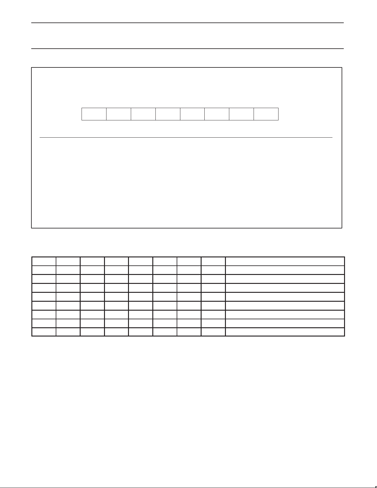
CCAPMn Address CCAPM0 0DAH
Not Bit Addressable
Bit:
Symbol Function
– Not implemented, reserved for future use*.
ECOMn Enable Comparator. ECOMn = 1 enables the comparator function.
CAPPn Capture Positive, CAPPn = 1 enables positive edge capture.
CAPNn Capture Negative, CAPNn = 1 enables negative edge capture.
MATn Match. When MATn = 1, a match of the PCA counter with this module’s compare/capture register causes the CCFn bit
TOGn Toggle. When T OGn = 1, a match of the PCA counter with this module’s compare/capture register causes the CEXn
PWMn Pulse Width Modulation Mode. PWMn = 1 enables the CEXn pin to be used as a pulse width modulated output.
ECCFn Enable CCF interrupt. Enables compare/capture flag CCFn in the CCON register to generate an interrupt.
NOTE:
*User software should not write 1s to reserved bits. These bits may be used in future 8051 family products to invoke new features. In that case, the reset or inactive value of the new
bit will be 0, and its active value will be 1. The value read from a reserved bit is indeterminate.
in CCON to be set, flagging an interrupt.
pin to toggle.
CCAPM1 0DBH
CCAPM2 0DCH
CCAPM3 0DDH
CCAPM4 0DEH
– ECOMn CAPPn CAPNn MATn TOGn PWMn ECCFn
76543210
Figure 7. CCAPMn: PCA Modules Compare/Capture Registers
80C575/83C575/
87C575
Reset Value = X000 0000B
SU00037
ECOMn CAPPn CAPNn MATn TOGn PWMn ECCFn MODULE FUNCTION
–
X 0 0 0 0 0 0 0 No operation
X X 1 0 0 0 0 X 16-bit capture by a positive-edge trigger on CEXn
X X 0 1 0 0 0 X 16-bit capture by a negative trigger on CEXn
X X 1 1 0 0 0 X 16-bit capture by a transition on CEXn
X 1 0 0 1 0 0 X 16-bit Software Timer
X 1 0 0 1 1 0 X 16-bit High Speed Output
X 1 0 0 0 0 1 0 8-bit PWM
X 1 0 0 1 X 0 X Watchdog Timer
Figure 8. PCA Module Modes (CCAPMn Register)
1998 May 01
13
Page 14
Philips Semiconductors Product specification
80C51 8-bit microcontroller family
8K/256 OTP/ROM/ROMless, 4 comparator, failure detect circuitry, watchdog timer
CF CR CCF4 CCF3 CCF2 CCF1 CCF0––
(TO CCFn)
CEXn
–– ECOMn CAPPn CAPNn MATn TOGn PWMn ECCFn
0 000
Figure 9. PCA Capture Mode
CAPTURE
80C575/83C575/
CCON
(D8H)
PCA TIMER/COUNTER
CH CL
CCAPnH CCAPnL
CCAPMn, n= 0 to 4
(DAH – DEH)
87C575
PCA INTERRUPT
SU00749
WRITE TO
CCAPnL
WRITE TO
CCAPnH
01
RESET
ENABLE
CF CR CCF4 CCF3 CCF2 CCF1 CCF0––
CCAPnH
16–BIT COMPARATOR
CH CL
PCA TIMER/COUNTER
–– ECOMn CAPPn CAPNn MATn TOGn PWMn ECCFn
CCAPnL
(TO CCFn)
MATCH
0000
Figure 10. PCA Compare Mode
CCON
(D8H)
PCA INTERRUPT
CCAPMn, n= 0 to 4
(DAH – DEH)
SU00750
1998 May 01
14
Page 15
Philips Semiconductors Product specification
80C51 8-bit microcontroller family
8K/256 OTP/ROM/ROMless, 4 comparator, failure detect circuitry, watchdog timer
CF CR CCF4 CCF3 CCF2 CCF1 CCF0––
WRITE TO
CCAPnL
WRITE TO
CCAPnH
01
RESET
ENABLE
CCAPnH CCAPnL
16–BIT COMPARATOR
CH CL
PCA TIMER/COUNTER
–– ECOMn CAPPn CAPNn MATn TOGn PWMn ECCFn
MATCH
(TO CCFn)
Figure 11. PCA High Speed Output Mode
80C575/83C575/
87C575
CCON
(D8H)
PCA INTERRUPT
TOGGLE
CEXn
CCAPMn, n: 0..4
(DAH – DEH)
1000
SU00751
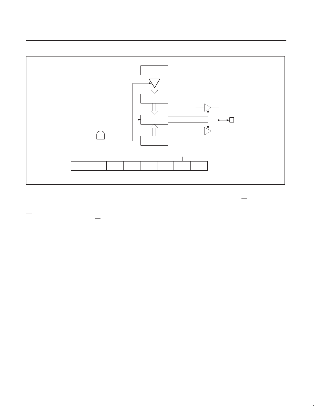
Pulse Width Modulator Mode
All of the PCA modules can be used as PWM
outputs. Figure 12 shows the PWM function.
The frequency of the output depends on the
source for the PCA timer. All of the modules
will have the same frequency of output
because they all share the PCA timer. The
duty cycle of each module is independently
variable using the module’s capture register
CCAPLn. When the value of the PCA CL
SFR is less than the value in the module’s
CCAPLn SFR the output will be low, when it
is equal to or greater than the output will be
high. When CL overflows from FF to 00,
CCAPLn is reloaded with the value in
CCAPHn. the allows updating the PWM
without glitches. The PWM and ECOM bits in
the module’s CCAPMn register must be set
to enable the PWM mode.
WATCHDOG TIMER
The watchdog timer is not directly loadable
by the user. Instead, the value to be loaded
into the main timer is held in an autoload
register or is part of the mask ROM
programming. In order to cause the main
timer to be loaded with the appropriate value,
a special sequence of software action must
take place. This operation is referred to as
feeding the watchdog timer.
To feed the watchdog, two instructions must
be sequentially executed successfully. No
intervening instruction fetches are allowed,
so interrupts should be disabled before
feeding the watchdog. The instructions
should move A5H to the WFEED1 register
and then 5AH to the WFEED2 register. If
WFEED1 is correctly loaded and WFEED2 is
not correctly loaded, then an immediate
underflow will occur.
The watchdog timer subsystem has two
modes of operation. Its principal function is a
watchdog timer. In this mode it protects the
system from incorrect code execution by
causing a system reset when the watchdog
timer underflows as a result of a failure of
software to feed the timer prior to the timer
reaching its terminal count. If the user does
not employ the watchdog function, the
watchdog subsystem can be used as a timer.
In this mode, reaching the terminal count sets
a flag. In most other respects, the timer mode
possesses the characteristics of the
watchdog mode. This is done to protect the
integrity of the watchdog function.
The watchdog timer subsystem consists of a
prescaler and a main counter. The prescaler
has 8 selectable taps off the final stages and
the output of a selected tap provides the
clock to the main counter. The main counter
is the section that is loaded as a result of the
software feeding the watchdog and it is the
section that causes the system reset
(watchdog mode) or time-out flag to be set
(timer mode) if allowed to reach its terminal
count.
Programming the Watchdog Timer
Both the EPROM and ROM devices have a
set of SFRs for holding the watchdog
autoload values and the control bits. The
watchdog time-out flag is present in the
watchdog control register and operates the
same in all versions. In the EPROM device,
the watchdog parameters (autoload value
and control) are always taken from the SFRs.
In the ROM device, the watchdog parameters
can be mask programmed or taken from the
SFRs. The selection to take the watchdog
parameters from the SFRs or from the mask
programmed values is controlled by EA
(external access). When EA is high (internal
ROM access), the watchdog parameters are
taken from the mask programmed values. If
the watchdog is mask programmed to the
timer mode, then the autoload values and the
pre-scaler taps are taken from the SFRs.
When EA is low (external access), the
watchdog parameters are taken from the
SFRs. The user should be able to leave code
in his program which initializes the watchdog
SFRs even though he has migrated to the
mask ROM part. This allows no code
changes from EPROM prototyping to ROM
coded production parts.
1998 May 01
15
Page 16
Philips Semiconductors Product specification
80C51 8-bit microcontroller family
8K/256 OTP/ROM/ROMless, 4 comparator, failure detect circuitry, watchdog timer
CCAPnH
CCAPnL
0
ENABLE
OVERFLOW
–– ECOMn CAPPn CAPNn MATn TOGn PWMn ECCFn
Figure 12. PCA PWM Mode
8–BIT
COMPARATOR
CL
PCA TIMER/COUNTER
0
CL < CCAPnL
CL >= CCAPnL
1
0000
80C575/83C575/
CEXn
CCAPMn, n: 0..4
(DAH – DEH)
SU00752
87C575
Watchdog Detailed Operation
EPROM Device (and ROMless Operation:
EA
= 0)
In the ROMless operation (ROM part, EA
and in the EPROM device, the watchdog
operates in the following manner (see
Figure 14).
Whether the watchdog is in the watchdog or
timer mode, when external RESET is applied,
the following takes place:
= 0)
•Watchdog mode bit set to watchdog mode.
•Watchdog run control bit set to ON.
•Autoload register set to 00 (min. count).
•Watchdog time-out flag cleared.
•Prescaler is cleared.
•Prescaler tap set to the highest divide.
•Autoload takes place.
The watchdog can be fed even though it is in
the timer mode.
Note that the operational concept is for the
watchdog mode of operation, when coming
out of a hardware reset, the software should
load the autoload registers, set the mode to
watchdog, and then feed the watchdog
(cause an autoload). The watchdog will now
be starting at a known point.
If the watchdog is in the watchdog mode and
running and happens to underflow at the time
the external RESET is applied, the watchdog
time-out flag will be cleared.
When the watchdog is in the watchdog mode
and the watchdog underflows, the following
action takes place (see Figure 16):
•Autoload takes place.
•Watchdog time-out flag is set
•Mode bit unchanged.
•Watchdog run bit unchanged.
•Autoload register unchanged.
•Prescaler tap unchanged.
•All other device action same as external
reset.
Note that if the watchdog underflows, the
program counter will start from 00H as in the
case of an external reset. The watchdog
time-out flag can be examined to determine if
the watchdog has caused the reset condition.
The watchdog time-out flag bit can be cleared
by software.
When the watchdog is in the timer mode and
the timer software underflows, the following
action takes place:
•Autoload takes place.
•Watchdog time-out flag is set
•Mode bit unchanged.
•Watchdog run bit unchanged.
•Autoload register unchanged.
•Prescaler tap unchanged.
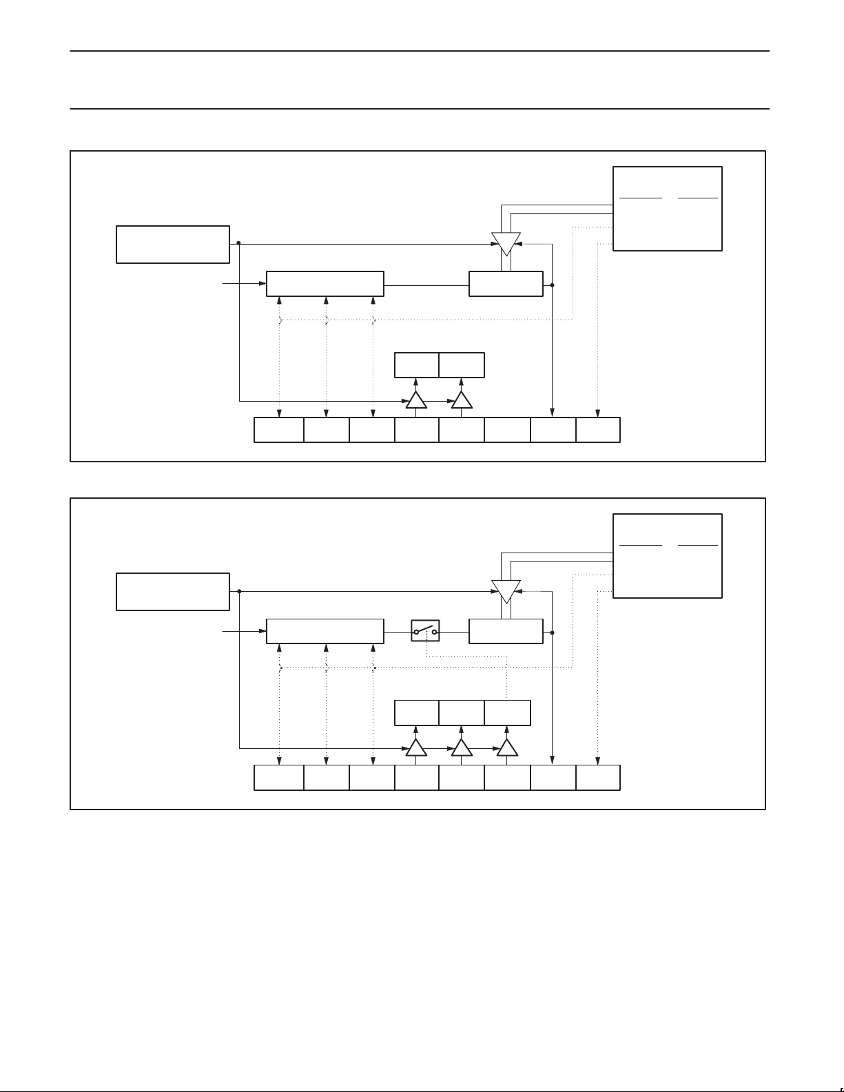
Mask ROM Device (EA = 1)
In the mask ROM device, the watchdog
mode bit (WDMOD) is mask programmed
and the bit in the watchdog command register
is read only and reflects the mask
programmed selection. If the mask
programmed mode bit selects the timer
mode, then the watchdog run bit (WDRUN)
operates as described under EPROM
Device. If the mask programmed bit selects
the watchdog mode, then the watchdog run
bit has no effect on the timer operation (see
Figure 15).
Watchdog Function
The watchdog consists of a programmable
prescaler and the main timer. The prescaler
derives its clock from the on-chip oscillator.
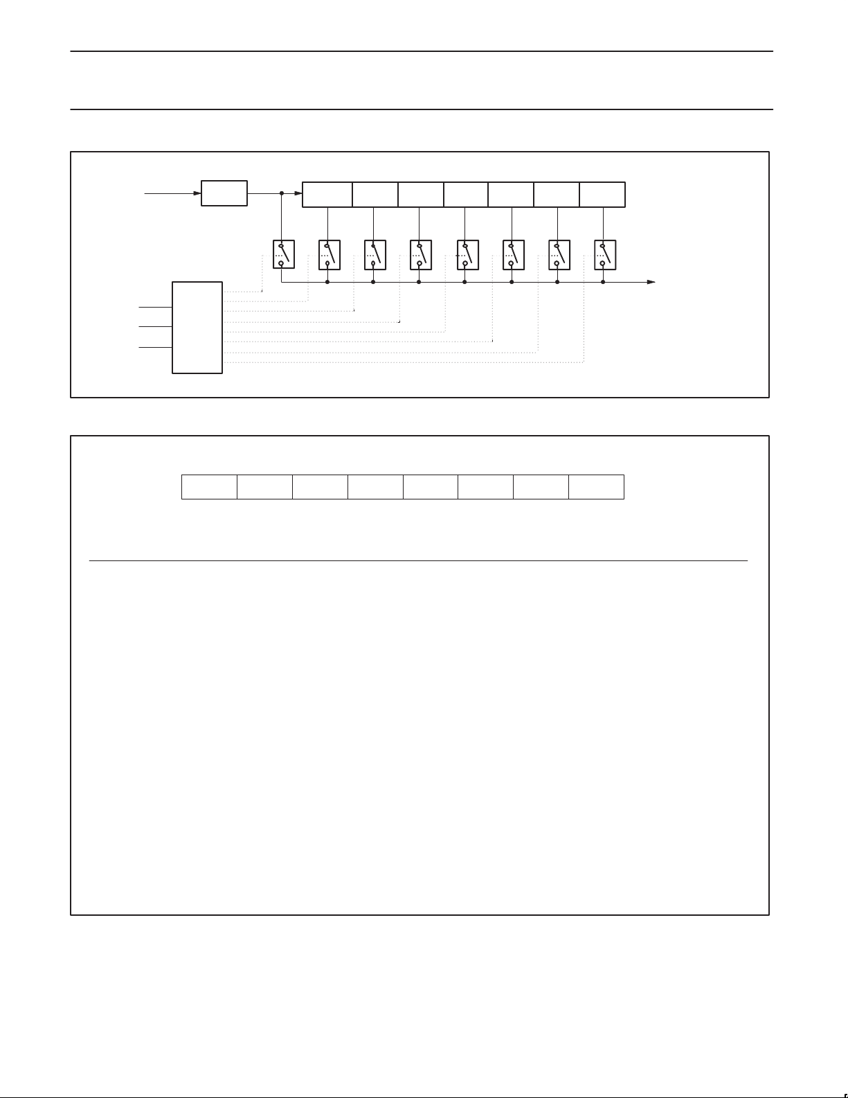
The prescaler consists of a divide by 12
followed by a 13 stage counter with taps from
stage 6 through stage 13. This is shown in
Figure 17. The tap selection is
programmable. The watchdog main counter
is a down counter clocked (decremented)
each time the programmable prescaler
underflows. The watchdog generates an
underflow signal (and is autoloaded) when
the watchdog is at count 0 and the clock to
decrement the watchdog occurs. The
watchdog is 8 bits long and the autoload
value can range from 0 to FFH. (The
autoload value of 0 is permissible since the
prescaler is cleared upon autoload).
This leads to the following user design
equations. Definitions :t
is the oscillator
OSC
1998 May 01
16
Page 17

Philips Semiconductors Product specification
80C51 8-bit microcontroller family
8K/256 OTP/ROM/ROMless, 4 comparator, failure detect circuitry, watchdog timer
period, N is the selected prescaler tap value,
W is the main counter autoload value, t
MIN
the minimum watchdog time-out value (when
the autoload value is 0), t
is the maximum
MAX
time-out value (when the autoload value is
FFH), t
is the design time-out value.
D
t
= t
= t
MIN
OSC
MIN
× 12 × 64
× 128 × 256
PRESCALER
× 2
× (W + 1)
MIN
t
MAX
tD = t
(where prescaler = 0, 1, 2, 3, 4, 5, 6, or 7)
Note that the design procedure is anticipated
to be as follows. A t
will be chosen either
MAX
from equipment or operation considerations
and will most likely be the next convenient
value higher than t
. (If the watchdog were
D
inadvertently to start from FFH, an overflow
would be guaranteed, barring other
anomalies, to occur within t
). Then the
MAX
value for the prescaler would be chosen
from:
prescaler = log2 (t
This then also fixes t
/ (t
MAX
MIN
× 12 × 256)) - 6
OSC
. An autoload value
would then be chosen from:
/ t
W = t
- 1
D
MIN
The software must be written so that a feed
operation takes place every t
seconds from
D
the last feed operation. Some tradeoffs may
need to be made. It is not advisable to
include feed operations in minor loops or in
subroutines unless the feed operation is a
specific subroutine.
Watchdog Control Register (WDCON)
(Bit Addressable) Address C0
The following bits of this register are read
only in the ROM part when EA
is high:
WDMOD, PRE0, PRE1, and PRE2. That is,
the register will reflect the mask programmed
values. In the ROM part with EA
high, these
bits are taken from mask coded bits and are
not readable by the program. WDRUN is
read only in the ROM part when EA
is high
and WDMOD is in the watchdog mode. When
WDMOD is in the timer mode, WDRUN
functions normally.
is
The parameters written into WDMOD, PRE0,
PRE1, and PRE2 by the program are not
applied directly to the watchdog timer
subsystem. The watchdog timer subsystem is
directly controlled by a second register which
stores these bits. The transfer of these bits
from the user register (WDMOD) to the
second control register takes place when the
watchdog is fed. This prevents random code
execution from directly foiling the watchdog
function. This does not affect the operation
where these bits are taken from mask coded
values.
The reset values of the WDCON and WDL
registers will be such that the timer resets to
the watchdog mode with a timeout period of
12 × 64 × 128 × t
. The watchdog timer
OSC
will not generate an interrupt. Additional bits
in WDCON are used to disable reset
generation by the oscillator fail and low
voltage detect circuits. WDCON can be
written by software only by executing a valid
watchdog feed sequence.
WDCON Register Bit Definitions
WDCON.7 PRE2 Prescaler Select 2,
reset to 1
WDCON.6 PRE1 Prescaler Select 1,
reset to 1
WDCON.5 PRE0 Prescaler Select 0,
reset to 1
WDCON.4 LVRE Low Voltage Reset
Enable, reset to 1
(enabled)
WDCON.3 OFRE Oscillator Fail Reset
Enable, reset to 1
(enabled)
WDCON.2 WDRUN Watchdog Run,
reset to 1 (enabled)
WDCON.1 WDTOF Watchdog Timeout
Flag, reset =
Indeterminate
WDCON.0 WDMOD Watchdog Mode,
reset to 1 (watchdog
mode)
80C575/83C575/
87C575
Enhanced UART
The UART operates in all of the usual modes
that are described in the first section of this
book for the 80C51. In addition the UART can
perform framing error detect by looking for
missing stop bits, and automatic address
recognition. The 87C575 UART also fully
supports multiprocessor communication as
does the standard 80C51 UART.
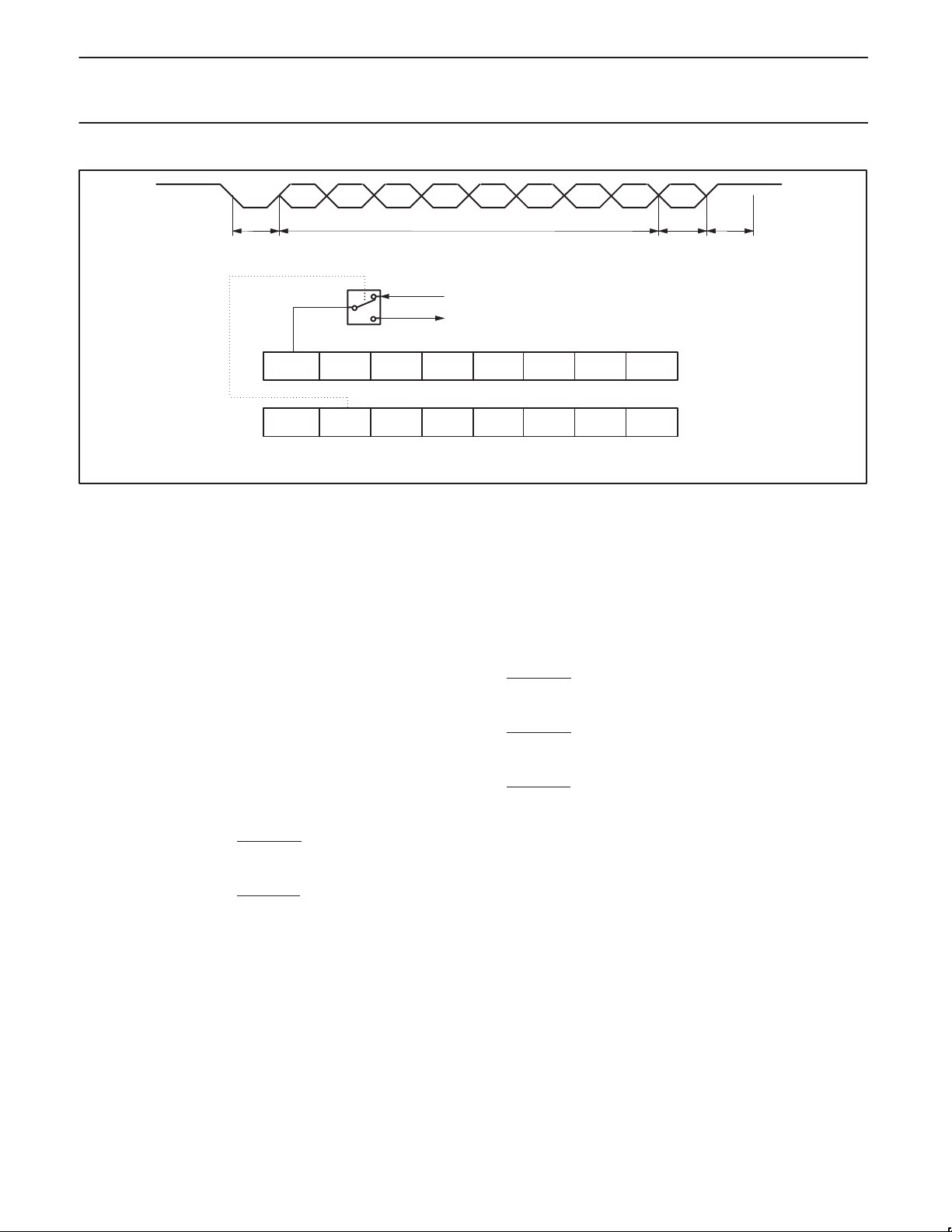
When used for framing error detect the UART
looks for missing stop bits in the
communication. A missing bit will set the FE
bit in the SCON register. The FE bit shares
the SCON.7 bit with SM0 and the function of
SCON.7 is determined by PCON.6 (SMOD0)
(see Figure 19). If SMOD0 is set then
SCON.7 functions as FE. SCON.7 functions
as SM0 when SMOD0 is cleared. When used
as FE SCON.7 can only be cleared by
software. Refer to Figure 18.
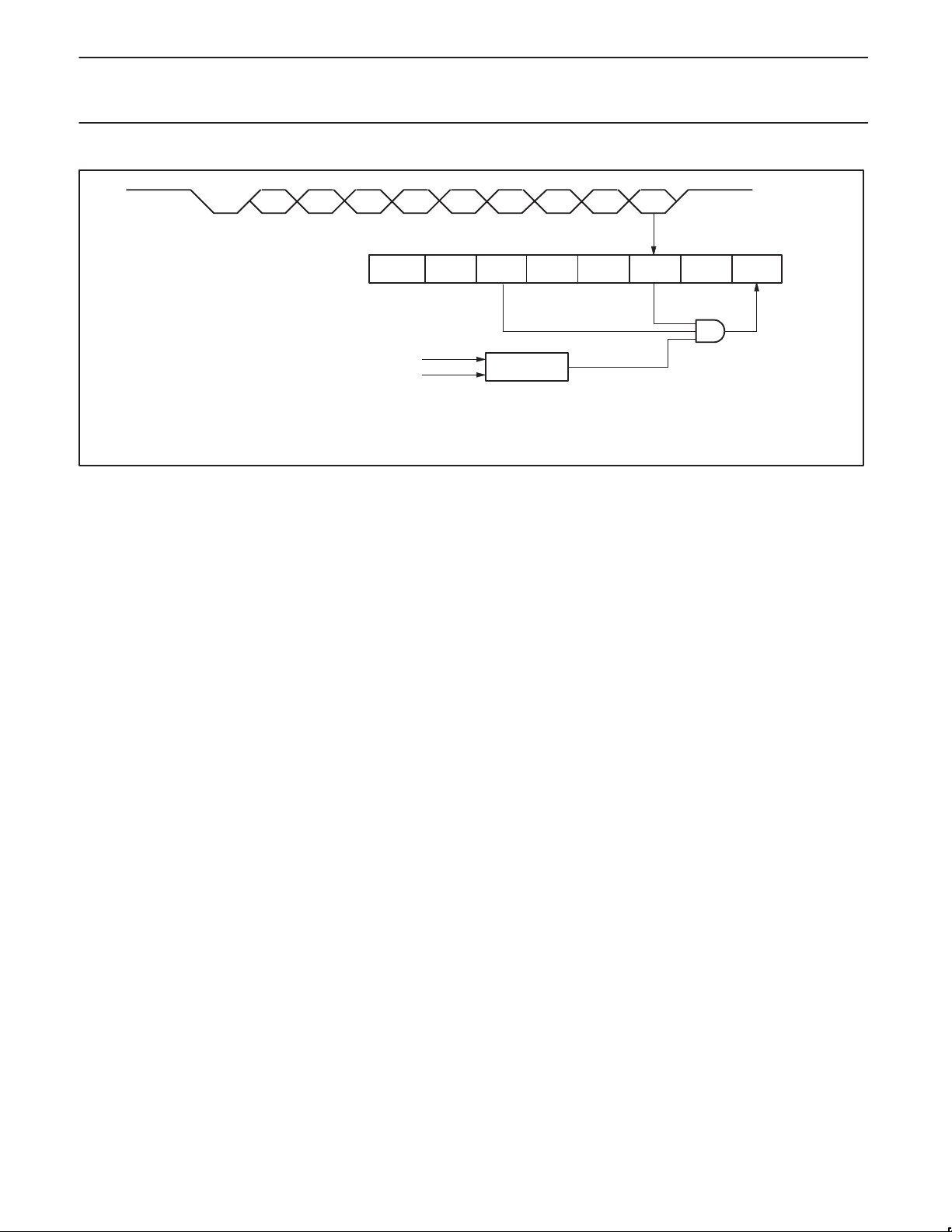
Automatic Address Recognition
Automatic Address Recognition is a feature
which allows the UART to recognize certain
addresses in the serial bit stream by using
hardware to make the comparisons. This
feature saves a great deal of software
overhead by eliminating the need for the
software to examine every serial address
which passes by the serial port. This feature
is enabled by setting the SM2 bit in SCON. In
the 9 bit UART modes, mode 2 and mode 3,
the Receive Interrupt flag (RI) will be
automatically set when the received byte
contains either the “Given” address or the
“Broadcast” address. The 9 bit mode requires
that the 9th information bit is a 1 to indicate
that the received information is an address
and not data. Automatic address recognition
is shown in Figure 20.
The 8 bit mode is called Mode 1. In this mode
the RI flag will be set if SM2 is enabled and
the information received has a valid stop bit
following the 8 address bits and the
information is either a Given or Broadcast
address.
Mode 0 is the Shift Register mode and SM2
is ignored.
1998 May 01
17
Page 18
Philips Semiconductors Product specification
80C51 8-bit microcontroller family
8K/256 OTP/ROM/ROMless, 4 comparator, failure detect circuitry, watchdog timer
CIDL WDTE –– –– –– CPS1 CPS0 ECF
WRITE TO
CCAP4L
WRITE TO
CCAP4H
01
RESET
ENABLE
CCAP4H CCAP4L
16–BIT COMPARATOR
CH CL
PCA TIMER/COUNTER
–– ECOMn CAPPn CAPNn MATn TOGn PWMn ECCFn
MATCH
1
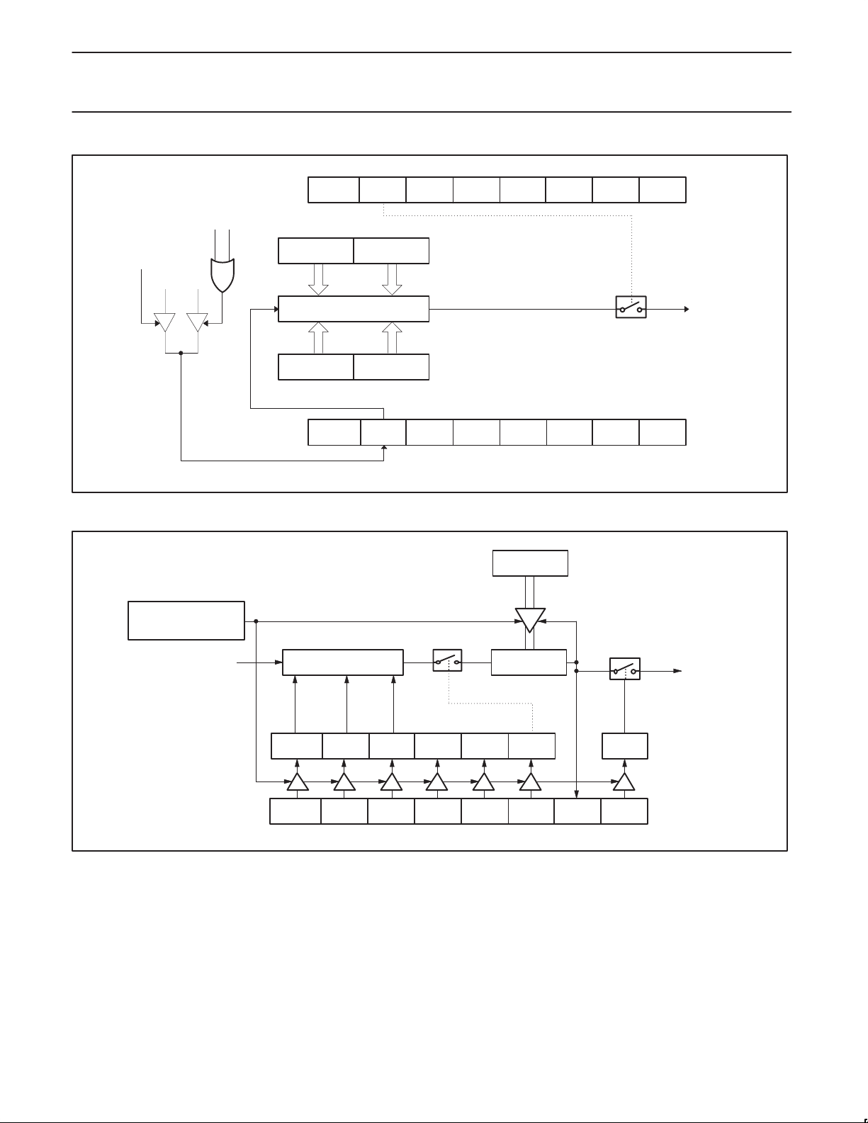
Figure 13. PCA Watchdog Timer
80C575/83C575/
87C575
CMOD
(D9H)
RESET
CCAPM4
(DEH)
X000
X
SU00042
WATCHDOG FEED SEQUENCE
MOV WFEED1,#0A5H
MOV WFEED2,#5AH
WDL (C1H)
PRESCALEROSC/12
PRE2 PRE1 PRE0 LVRE OFRE WDRUN WDTOF WDMOD
8–BIT DOWN
COUNTER
Figure 14. Watchdog Timer in 87C575 and 80C575 / 83C575 (EA = 0)
RESET
SHADOW REGISTER
FOR WDCON
WDCON
(C0H)
SU00240
1998 May 01
18
Page 19
Philips Semiconductors Product specification
80C51 8-bit microcontroller family
8K/256 OTP/ROM/ROMless, 4 comparator, failure detect circuitry, watchdog timer
WATCHDOG FEED SEQUENCE
MOV WFEED1,#0A5H
MOV WFEED2,#5AH
PRESCALEROSC/12
SHADOW REGISTER
FOR WDCON
PRE2 PRE1 PRE0 LVRE OFRE WDRUN WDTOF WDMOD
Figure 15. Watchdog Timer of 83C575 in Watchdog Mode (EA = 1, WDMOD = 1)
8–BIT DOWN
COUNTER
80C575/83C575/
87C575
ROM–CODE
ADDRESS
2032H
2031H
2030H
SU00241
1
CONTENT
WD
PRE2:0
WDMOD
WDCON
(C0H)
WATCHDOG FEED SEQUENCE
MOV WFEED1,#0A5H
MOV WFEED2,#5AH
PRESCALEROSC/12
SHADOW REGISTER
FOR WDCON
PRE2 PRE1 PRE0 LVRE OFRE WDRUN WDTOF WDMOD
8–BIT DOWN
COUNTER
0
Figure 16. Watchdog Timer of 83C575 in Timer Mode (EA = 1, WDMOD = 0)
ROM–CODE
CONTENT
WD
PRE2:0
WDMOD
WDCON
(C0H)
ADDRESS
2032H
2031H
2030H
SU00242
1998 May 01
19
Page 20
Philips Semiconductors Product specification
80C51 8-bit microcontroller family
8K/256 OTP/ROM/ROMless, 4 comparator, failure detect circuitry, watchdog timer
OSC/12 ÷64
PRE2
PRE1
PRE0
DECODE
SCON Address = 98H
Bit Addressable
SM0/FE SM1 SM2 REN TB8 RB8 Tl Rl
Bit: 76543210
(SMOD0 = 0/1)*
÷64 ÷128 ÷256 ÷512 ÷1024 ÷2048 ÷4096 ÷8192
000
001
010
011
100
101
110
111
÷2 ÷2 ÷2 ÷2 ÷2 ÷2 ÷2
Figure 17. Watchdog Prescaler
80C575/83C575/
87C575
TO WATCHDOG
DOWN COUNTER
SU00243
Reset Value = 0000 0000B
Symbol Function
FE Framing Error bit. This bit is set by the receiver when an invalid stop bit is detected. The FE bit is not cleared by valid
frames but should be cleared by software. The SMOD0 bit must be set to enable access to the FE bit.
SM0 Serial Port Mode Bit 0, (SMOD0 must = 0 to access bit SM0)
SM1 Serial Port Mode Bit 1
SM0 SM1 Mode Description Baud Rate**
0 0 0 shift register f
OSC
/12
0 1 1 8-bit UART variable
1 0 2 9-bit UART f
OSC
/64 or f
OSC
/32
1 1 3 9-bit UART variable
SM2 Enables the Automatic Address Recognition feature in Modes 2 or 3. If SM2 = 1 then Rl will not be set unless the
received 9th data bit (RB8) is 1, indicating an address, and the received byte is a Given or Broadcast Address.
In Mode 1, if SM2 = 1 then Rl will not be activated unless a valid stop bit was received, and the received byte is a
Given or Broadcast Address. In Mode 0, SM2 should be 0.
REN Enables serial reception. Set by software to enable reception. Clear by software to disable reception.
TB8 The 9th data bit that will be transmitted in Modes 2 and 3. Set or clear by software as desired.
RB8 In modes 2 and 3, the 9th data bit that was received. In Mode 1, if SM2 = 0, RB8 is the stop bit that was received.
In Mode 0, RB8 is not used.
Tl Transmit interrupt flag. Set by hardware at the end of the 8th bit time in Mode 0, or at the beginning of the stop bit in the
other modes, in any serial transmission. Must be cleared by software.
Rl Receive interrupt flag. Set by hardware at the end of the 8th bit time in Mode 0, or halfway through the stop bit time in
the other modes, in any serial reception (except see SM2). Must be cleared by software.
NOTE:
*SMOD0 is located at PCON6.
= oscillator frequency
**f
OSC
Figure 18. SCON: Serial Port Control Register
SU00043
1998 May 01
20
Page 21
Philips Semiconductors Product specification
80C51 8-bit microcontroller family
8K/256 OTP/ROM/ROMless, 4 comparator, failure detect circuitry, watchdog timer
D0 D1 D2 D3 D4 D5 D6 D7 D8
START
BIT
SM0 / FE SM1 SM2 REN TB8 RB8 TI RI
SMOD1 SMOD0 – POF LVF GF0 GF1 IDL
0 : SCON.7 = SM0
1 : SCON.7 = FE
Figure 19. UART Framing Error Detection
DATA BYTE
SET FE BIT IF STOP BIT IS 0 (FRAMING ERROR)
SM0 TO UART MODE CONTROL
80C575/83C575/
87C575
ONLY IN
MODE 2, 3
SCON
(98H)
PCON
(87H)
STOP
BIT
SU00044
Using the Automatic Address Recognition
feature allows a master to selectively
communicate with one or more slaves by
invoking the Given slave address or
addresses. All of the slaves may be
contacted by using the Broadcast address.
Two special Function Registers are used to
define the slave’s address, SADDR, and the
address mask, SADEN. SADEN is used to
define which bits in the SADDR are to b used
and which bits are “don’t care”. The SADEN
mask can be logically ANDed with the
SADDR to create the “Given” address which
the master will use for addressing each of the
slaves. Use of the Given address allows
multiple slaves to be recognized while
excluding others. The following examples will
help to show the versatility of this scheme:
Slave 0 SADDR = 1100 0000
SADEN = 1111 1101
Given = 1100 00X0
Slave 1 SADDR = 1100 0000
SADEN = 1111 1110
Given = 1100 000X
In the above example SADDR is the same
and the SADEN data is used to differentiate
between the two slaves. Slave 0 requires a 0
in bit 0 and it ignores bit 1. Slave 1 requires a
0 in bit 1 and bit 0 is ignored. A unique
address for Slave 0 would be 1100 0010
since slave 1 requires a 0 in bit 1. A unique
address for slave 1 would be 1100 0001
since a 1 in bit 0 will exclude slave 0. Both
slaves can be selected at the same time by
an address which has bit 0 = 0 (for slave 0)
and bit 1 = 0 (for slave 1). Thus, both could
be addressed with 1100 0000.
In a more complex system the following could
be used to select slaves 1 and 2 while
excluding slave 0:
Slave 0 SADDR = 1100 0000
SADEN = 1111 1001
Given = 1100 0XX0
Slave 1 SADDR = 1110 0000
SADEN = 1111 1010
Given = 11 10 0X0X
Slave 2 SADDR = 1110 0000
SADEN = 1111 1100
Given = 1110 00XX
In the above example the differentiation
among the 3 slaves is in the lower 3 address
bits. Slave 0 requires that bit 0 = 0 and it can
be uniquely addressed by 1110 0110. Slave 1
requires that bit 1 = 0 and it can be uniquely
addressed by 1110 and 0101. Slave 2
requires that bit 2 = 0 and its unique address
is 1110 0011. To select Slaves 0 and 1 and
exclude Slave 2 use address 1110 0100,
since it is necessary t make bit 2 = 1 to
exclude slave 2.
The Broadcast Address for each slave is
created by taking the logical OR of SADDR
and SADEN. Zeros in this result are treated
as don’t-cares. In most cases, interpreting
the don’t-cares as ones, the broadcast
address will be FF hexadecimal.
Upon reset SADDR (SFR address 0A9H) and
SADEN (SFR address 0B9H) are loaded with
0s. This produces a given address of all
“don’t cares” as well as a Broadcast address
of all “don’t cares”. this effectively disables
the Automatic Addressing mode and allows
the microcontroller to use standard 80C51
type UART drivers which do not make use of
this feature.
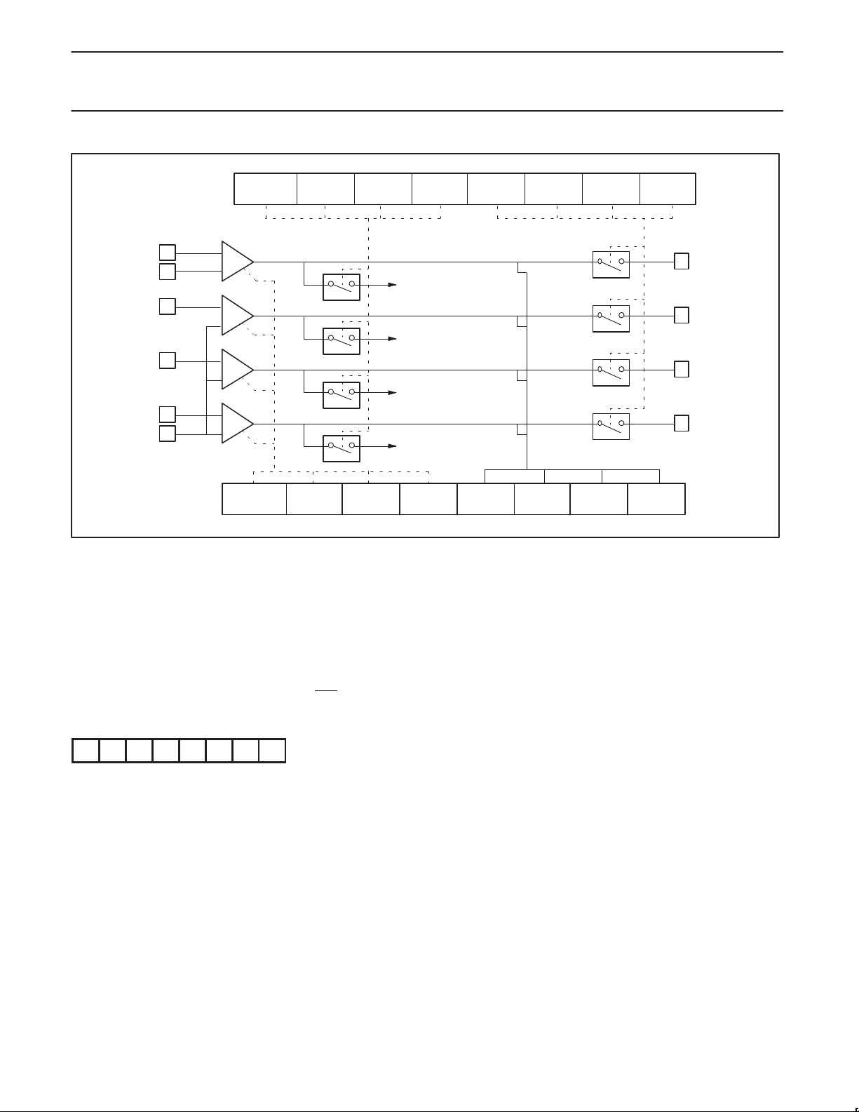
Analog Comparators
Four analog comparators are provided on
chip. Three comparators have a common
negative reference CMPR- and independent
positive inputs CMP1+, CMP2+, CMP3+ on
port 3. The fourth comparator has
independent positive and negative inputs
CMP0+ and CMP0- on port 1. The CMP
register contains an output and enable bit for
each comparator. The CMP register is bit
addressable and is located at SFR address
E8H. Figure 21 shows the connection of the
comparators.
Pullups at the comparator input pins will be
disabled by hardware when the comparator is
enabled. In addition, to make inputs high
impedance, the corresponding port SFR bits
must be set by software to disable the
pulldowns.
1998 May 01
21
Page 22
Philips Semiconductors Product specification
80C51 8-bit microcontroller family
8K/256 OTP/ROM/ROMless, 4 comparator, failure detect circuitry, watchdog timer
D0 D1 D2 D3 D4 D5 D6 D7 D8
SM0 SM1 SM2 REN TB8 RB8 TI RI
11 X
COMPARATOR
RECEIVED ADDRESS D0 TO D7
PROGRAMMED ADDRESS
IN UART MODE 2 OR MODE 3 AND SM2 = 1:
INTERRUPT IF REN=1, RB8=1 AND “RECEIVED ADDRESS” = “PROGRAMMED ADDRESS”
– WHEN OWN ADDRESS RECEIVED, CLEAR SM2 TO RECEIVE DATA BYTES
– WHEN ALL DATA BYTES HAVE BEEN RECEIVED: SET SM2 TO WAIT FOR NEXT ADDRESS.
Figure 20. UART Multiprocessor Communication, Automatic Address Recognition
CMP Register Bit Definitions
CMP.7 enable comparator 3,
disable pullups at P3.4, P3.7
CMP.6 enable comparator 2,
disable pullups at P3.4, P3.6
CMP.5 enable comparator 1,
disable pullups at P3.4, P3.5
CMP.4 enable comparator 0,
disable pullups at P1.0, P1.1
CMP.3 comparator 3 output (read only)
CMP.2 comparator 2 output (read only)
CMP.1 comparator 1 output (read only)
CMP.0 comparator 0 output (read only)
All comparators are disabled automatically in
power down mode, in idle mode unused
comparators should be disabled by software
to save power. A comparator can generate
an interrupt that will terminate idle mode.
The CMPE register contains bits to enable
each comparator to drive external output pins
or internal PCA capture inputs. Pullups at the
output pins are disabled by hardware when
the external comparator output is enabled.
The comparator output is wire-ORed with the
corresponding port SFR bit, so the SFR bit
must also be set by software to enable the
output.
1
1
1
0
CMPE Register Bit Definitions
CMPE.7 enables comparator 3 to drive
CEX3
CMPE.6 enables comparator 2 to drive
CEX2
CMPE.5 enables comparator 1 to drive
CEX1
CMPE.4 enables comparator 0 to drive
CEX0
CMPE.3 enables comparator 3 output on
P1.6 (open drain)
CMPE.2 enables comparator 2 output on
P1.5 (open drain)
CMPE.1 enables comparator 1 output on
P1.4 (open drain)
CMPE.0 enables comparator 0 output on
P1.3 (open drain)
When 1s are written to CMPE bits 7-4,
the comparator outputs will drive the
corresponding capture input. (This function is
not available in the idle or power-down
mode.) When 1s are written to CMPE bits 3-0
the comparator output will also drive the
corresponding port 1 pin. (This function is
available in idle mode.) If the comparator’s
enabled to drive the capture input but not the
port pin, then the port pin can be used for
general purpose I/O. When a comparator
output is enabled, pullups at the output pin
are disabled and the output becomes open
drain. The comparator output can be used to
trigger a capture input in idle mode by
programming the CMPE register to drive the
80C575/83C575/
87C575
SCON
(98H)
SU00045
pin from the comparator output to have the
pin supply the capture trigger.
There are two special function registers
associated with the comparators. They are
CMP which contains the comparator enables
and a bit that can be read by software to
determine the state of each comparator’s
output, and CMPE which controls whether
the output from each comparator drives the
associated output pin or a capture input
associated with one of the PCA modules.
The CMP registers bits 0–3 can be read by
software to determine the state of the output
of each comparator. To do this the associated
comparator must be enabled but the output in
port 1 can be disabled. This allows easy
polling of the comparator output value without
the need to use up a port pin.
The CMPE register allows the comparator to
drive the associated PCA module capture
input, so that on compare a capture can be
generated in the PCA. Bits 0–3 of this
register enable the comparator output to drive
the associated port 1 output circuitry. Used
as a comparator output this circuitry is open
drain. To enable the comparator output to
drive to port 1, the corresponding port bit
must also be set to disable the pulldown. If
the comparator is not enabled to drive the
port 1 circuitry, the associated port 1 pin can
be used for other I/O. This includes when a
comparator is enabled to drive the capture
input to a PCA module.
1998 May 01
22
Page 23
Philips Semiconductors Product specification
80C51 8-bit microcontroller family
8K/256 OTP/ROM/ROMless, 4 comparator, failure detect circuitry, watchdog timer
EC3TDC EC2TDC EC1TDC EC0TDC EC3OD * EC2OD * EC1OD * EC0OD *
P1.0 / CMP0+
P1.1 / CMP0–
P3.5 / CMP1+
P3.6 / CMP2+
P3.7 / CMP3+
P3.4 / CMPR–
+
–
ENABLE
+
–
ENABLE
+
–
ENABLE
+
–
ENABLE
TO CEX0 INPUT OF
PCA MODULE 0
TO CEX1 INPUT OF
PCA MODULE 1
TO CEX2 INPUT OF
PCA MODULE 2
TO CEX3 INPUT OF
PCA MODULE 3
80C575/83C575/
87C575
CMPE
(91H)
P1.3 / CMP0
P1.4 / CMP1
P1.5 / CMP2
P1.6 / CMP3
* : WILL DISABLE PULLUPS
ON RELEVANT PINS
EC3DP * EC2DP * EC1DP * EC0DP * C3R0 C2R0 C1R0 C0R0
Reduced EMI Mode
There are two bits in the AUXR register that
can be set to reduce the internal clock drive
and disable the ALE output. AO (AUXR.0)
when set turns off the ALE output. LO
(AUXR.1) when set reduces the drive of the
internal clock circuitry. Both bits are cleared
on Reset. With LO set the 87C575 will still
operate at 12MHz, but will have reduced EMI
in the range above 100MHz.
AUXR (8EH)
–– –– –– –– –– –– LO AO
AO: Turns off ALE output.
LO: Reduces drive of internal clock
circuitry. 8XC575 spec’d to 12MHz
when LO set.
Figure 21. Analog Comparators
INTERNAL RESET
Internal resets generated by the power on,
low voltage, and oscillator fail detect circuits
are self timed to guarantee proper
initialization of the 8XC575. Reset will be held
approximately 24 oscillator periods after
normal conditions are detected by all enabled
detect circuits. Internal resets do not drive
RST
but will cause missing pulses on ALE.
Interrupt Enable (IE) Register
EA IE.7 enable all interrupts
EC IE.6 enable PCA interrupt
ET2 IE.5 enable Timer 2 interrupt
ES IE.4 enable Serial I/O interrupt
ET1 IE.3 enable Timer 1 interrupt
EX1 IE.2 enable External interrupt 1
ET0 IE.1 enable Timer 0 interrupt
EX0 IE.0 enable External interrupt 0
CMP
(E8H)
SU00244
Interrupt Priority (IP) Register
IP.7 reserved
PPC IP .6 PCA interrupt priority
PT2 IP.5 Timer 2 interrupt priority
PS IP.4 Serial I/O interrupt priority
PT1 IP.3 Timer 1 interrupt priority
PX1 IP.2 External interrupt 1 priority
PT0 IP.1 Timer 0 interrupt priority
PX0 IP.0 External interrupt 0 priority
Priority Source Flag Vector
1 INT0 IE0 03H highest priority
Timer 0
2
TF0 0BH
3 INT1 IE1 13H
4
Timer 1
TF1 1BH
87C575
5 PCA
6
Serial I/O
Timer 2 TF2/EXF2
7
CF,CCFn
33H
RI,TI 23H
2BH lowest priority
80C575/83C575/87C575
5
Serial I/O RI/TI
Timer 2 TF2/EXF2
6
7
PCA CF, CCFn33H lowest priority
23H
23H
Power Control (PCON) Register
SMOD1 PCON.7 double baud rate bit
SMOD0 PCON.6 SCON.7 access control
OSF PCON.5 oscillator fail flag
POF PCON.4 power off flag
LVF PCON.3 low voltage flag
GF0 PCON.2 general purpose flag
PD PCON.1 power down mode bit
IDL PCON.0 idle mode bit
Port 2 Pullup Disable Register
1998 May 01
23
Page 24

Philips Semiconductors Product specification
80C51 8-bit microcontroller family
8K/256 OTP/ROM/ROMless, 4 comparator, failure detect circuitry, watchdog timer
OSCILLATOR CHARACTERISTICS
XTAL1 and XTAL2 are the input and output,
respectively, of an inverting amplifier. The
pins can be configured for use as an on-chip
oscillator, as shown in the Logic Symbol,
page 4.
To drive the device from an external clock
source, XTAL1 should be driven while XTAL2
is left unconnected. There are no
requirements on the duty cycle of the
external clock signal, because the input to
the internal clock circuitry is through a
divide-by-two flip-flop. However, minimum
and maximum high and low times specified in
the data sheet must be observed.
IDLE MODE
In idle mode, the CPU puts itself to sleep
while all of the on-chip peripherals stay
active. The instruction to invoke the idle
mode is the last instruction executed in the
normal operating mode before the idle mode
is activated. The CPU contents, the on-chip
RAM, and all of the special function registers
remain intact during this mode. The idle
mode can be terminated either by any
enabled interrupt (at which time the process
is picked up at the interrupt service routine
and continued), or by a hardware reset which
starts the processor in the same manner as a
power-on reset.
80C575/83C575/
87C575
POWER-DOWN MODE
In the power-down mode, the oscillator is
stopped and the instruction to invoke
power-down is the last instruction executed.
Only the contents of the on-chip RAM are
preserved. The control bits for the reduced
power modes are in the special function
register PCON. Power-down mode can be
terminated with either a hardware reset or
external interrupt. With an external interrupt
INT0
or INT1 must be enabled and
configured as level sensitive. Holding the pin
low restarts to oscillator and bringing the pin
back high completes the exit.
If the watchdog is enabled (WDRUN = 1),
then power-down mode is disabled.
DESIGN CONSIDERATIONS
At power-on, the voltage on VCC must come
up with RST
Table 2 shows the state of I/O ports during
low current operating modes.
low for a proper start-up.
Table 2. External Pin Status During Idle and Power-Down Modes
MODE PROGRAM MEMORY ALE PSEN PORT 0 PORT 1 PORT 2 PORT 3
Idle Internal 1 1 Data Data Data Data
Idle External 1 1 Float Data Address Data
Power-down Internal 0 0 Data Data Data Data
Power-down External 0 0 Float Data Data Data
1998 May 01
24
Page 25
Philips Semiconductors Product specification
80C51 8-bit microcontroller family
80C575/83C575/
8K/256 OTP/ROM/ROMless, 4 comparator, failure detect circuitry, watchdog timer
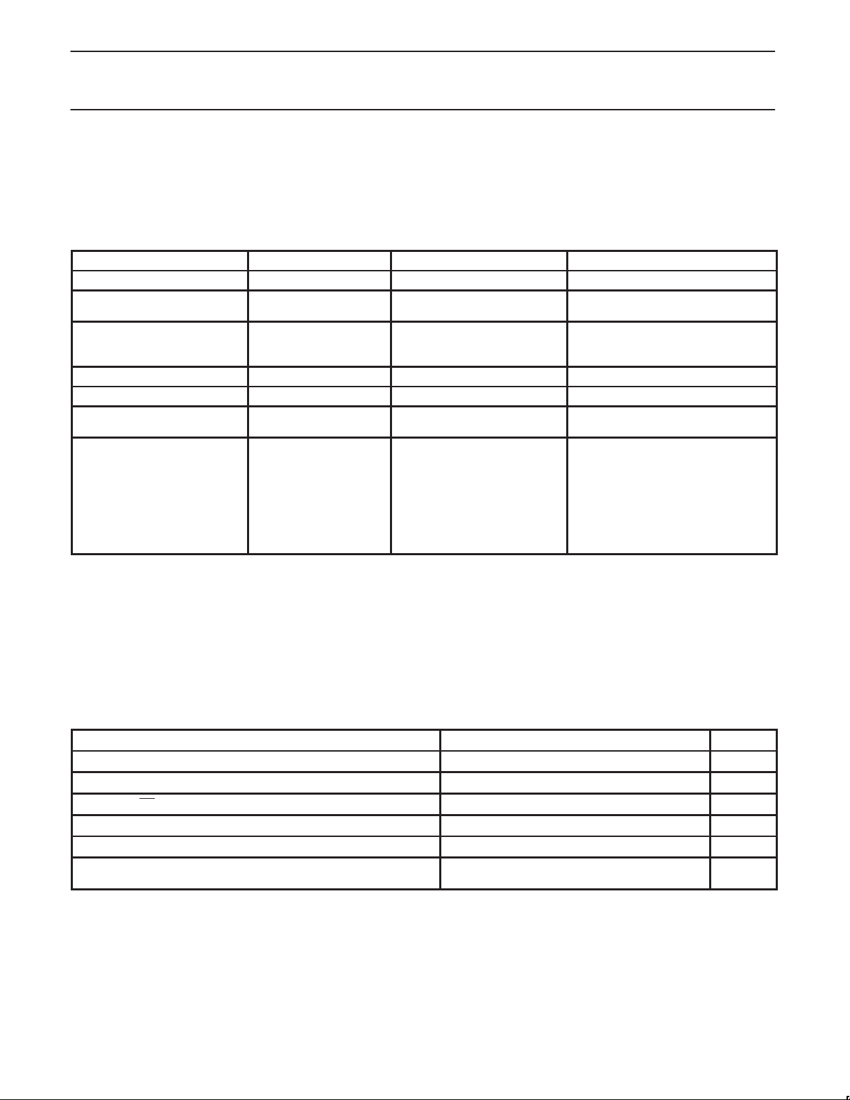
ROM CODE SUBMISSION
When submitting ROM code for the 83C575, the following must be specified:
1. 8k byte user ROM data
2. 32 byte ROM encryption key
3. ROM security bits
4. The watchdog timer parameters.
ADDRESS
0000H to 1FFFH DATA 7:0 User ROM Data
2000H to 201FH KEY 7:0 ROM Encryption Key
2020H Reserved
2030H Reserved 7:0 Must = FFH
2031H Reserved 7:0 Must = FFH
2032H WDL
2033H WDCON
2033H WDCON
2033H WDCON
2033H WDCON
2033H WDCON
2033H WDCON
NOTES:
1. See Watchdog Timer Specification for definition of WDL and WDCON bits.
CONTENT BIT(S) COMMENT
FFH = no encryption
Security Bit 2
Security Bit 1
1
1
1
1
1
1
1
2
1
0
7:0 Watchdog reload value
7:5 PRE2:0
4 LVRE
3 OFRE
2 WDRUN=0, not ROM coded
1 WDTOF=0, not ROM coded
0 WDMOD
Must = 1
0 = enable, 1 = disable
0 = enable, 1 = disable
(see specification)
87C575
Security Bit 1: When programmed, this bit has two effects on masked ROM parts:
1. External MOVC is disabled, and
2. EA# is latched on Reset.
Security Bit 2: When programmed, this bit inhibits Verify User ROM.
ABSOLUTE MAXIMUM RATINGS
PARAMETER
Operating temperature under bias –55 to +125 °C
Storage temperature range –65 to +150 °C
Voltage on EA/VPP pin to V
Voltage on any other pin to V
Maximum IOL per I/O pin 15 mA
Power dissipation (based on package heat transfer limitations, not
device power consumption)
NOTES:
1. Stresses above those listed under Absolute Maximum Ratings may cause permanent damage to the device. This is a stress rating only and
functional operation of the device at these or any conditions other than those described in the AC and DC Electrical Characteristics section
of this specification is not implied.
2. This product includes circuitry specifically designed for the protection of its internal devices from the damaging effects of excessive static
charge. Nonetheless, it is suggested that conventional precautions be taken to avoid applying greater than the rated maxima.
3. Parameters are valid over operating temperature range unless otherwise specified. All voltages are with respect to V
noted.
SS
SS
1, 2, 3
RATING UNIT
0 to +13.0 V
–0.5 to +6.5 V
1.5 W
unless otherwise
SS
1998 May 01
25
Page 26
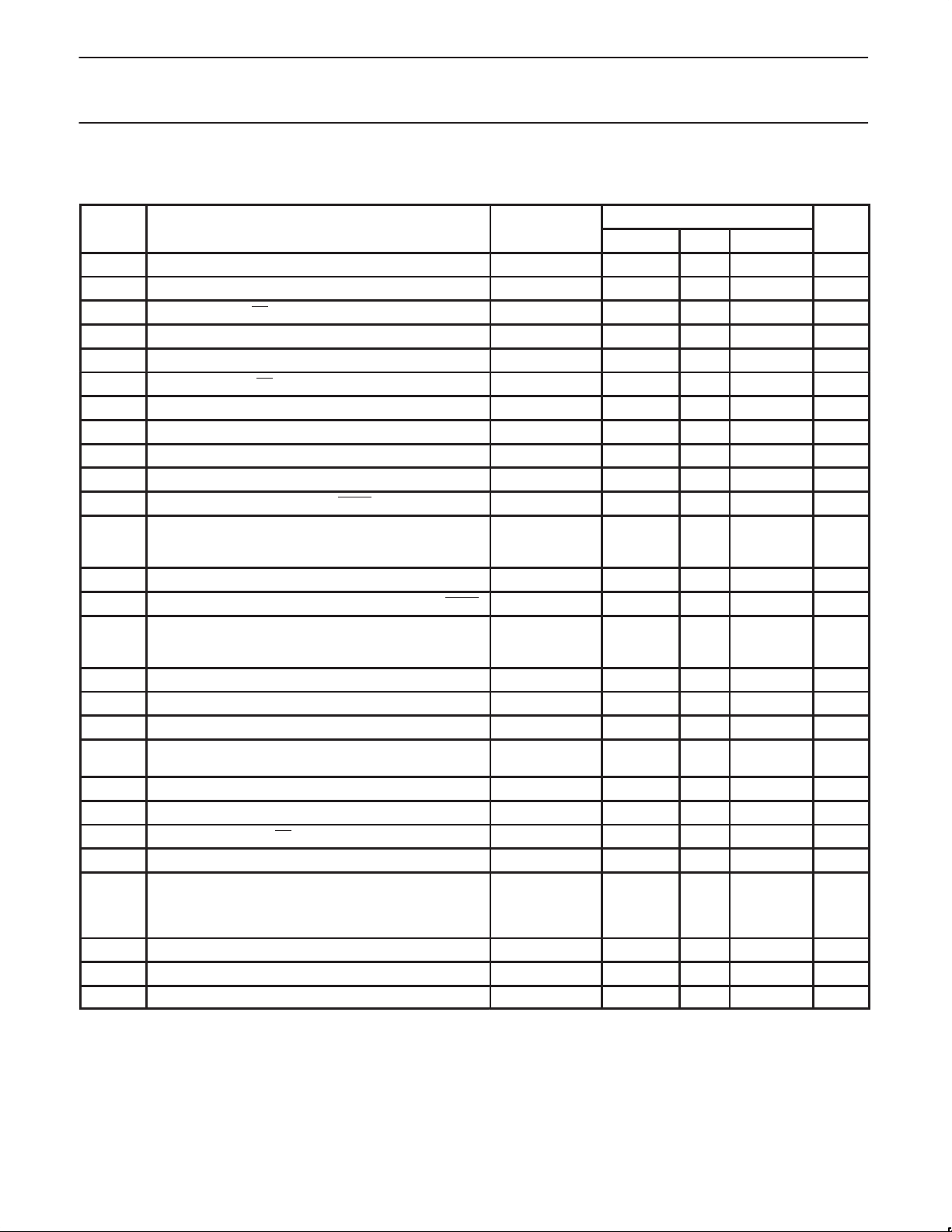
Philips Semiconductors Product specification
SYMBOL
PARAMETER
UNIT
80C51 8-bit microcontroller family
8K/256 OTP/ROM/ROMless, 4 comparator, failure detect circuitry, watchdog timer
80C575/83C575/
87C575
DC ELECTRICAL CHARACTERISTICS
T
= 0°C to +70°C and –40°C to +125°C, VCC = 5V ±10%, VSS = 0V
amb
CC
LIMITS
1
20
8
5
MAX
VCC+0.5 V
0.50
0.45
CC
30
12
75
TEST
CONDITIONS
V
IL
V
IL1
V
IL2
V
IH
V
IH1
V
IH2
V
IH3
Input low voltage (Ports 0, 2, 3, except 3.2, 3.3) –0.5 0.5VCC–0.6 V
Input low voltage (Ports 1, 3.2, 3.3, XTAL1, RST) –0.5 0.2VCC–0.5 V
Input low voltage (EA) 0 0.2VCC–0.45 V
Input high voltage (Ports 0, 2, 3, except 3.2, 3.3) 0.5VCC+0.8 VCC+0.5 V
Input high voltage (Ports 1, 3.2, 3.3) 0.8VCC+0.3 VCC+0.5 V
Input high voltage (EA) 0.2VCC+0.9 VCC+0.5 V
Input high voltage (XTAL1, RST) 0.7V
MIN TYP
HYS Hysteresis (Ports 0, 2, 3, except 3.2, 3.3) 200 mV
HYS1 Hysteresis (Ports 1, 3.2, 3.3) 50 mV
V
V
V
V
V
V
V
V
I
IL
I
TL
I
TL1
I
L1
I
L2
I
LC
I
CC
OL
OL1
OL2
OH
OH1
OH2
IO
CR
Output voltage low (Ports 1, 2, 3, except 3.1) IOL = 1.6mA 0.45 V
Output voltage low (Ports 0, ALE, PSEN
)
IOL = 3.2mA 0.45 V
Output voltage low
P3.1 with bit cleared
P3.1 with bit set
IOL = 10.0mA
I
= 1.6mA
OL
Output voltage high (Ports 1, 2, 3, except P3.1) IOH = –30µA VCC–0.7 V
Output voltage high (Port 0 in external bus mode, ALE, PSEN) IOH = –3.2mA VCC–0.7 V
Output voltage high
P3.1 with bit cleared
P3.1 with bit set
IOH = –10.0mA
I
= –1.6mA
OH
VCC–1.5
VCC–1.5
Offset voltage comparator inputs –35 +35 mV
Common mode range comparator inputs 0 V
Logical 0 input current (Ports 1, 2, 3, except 3.1) VIN = 0.45V –75 µA
Logical 1-to-0 transition current
(Ports 2, 3, except 3.1, 3.2, 3.3)
4
See Note 4 –600 µA
Logical 1-to-0 transition current (Ports 1, 3.2, 3.3) See Note 4 –450 µA
Input leakage current (Port 0, Port2 in open drain mode)
Input leakage current (EA, P3.1) 0.45 < VIN < V
Input leakage current comparator inputs 0 < VIN < V
Power supply current:
Active mode @ 16MHz
7
5
9
0.45 < VIN < V
See note 6
CC
CC
CC
2 40 µA
–10 +10 µA
–1.0 +1.0 µA
Idle mode @ 16MHz
Power-down mode
R
V
C
RST
LOW
IO
Internal reset pull-up resistor VIN = 0V 50 200 kΩ
Low VCC detect voltage 4.0 4.45 V
Pin capacitance
10
f = 1MHz 10 pF
NOTES: (SEE NEXT PAGE)
V
V
V
V
V
mA
mA
µA
1998 May 01
26
Page 27

Philips Semiconductors Product specification
80C51 8-bit microcontroller family
8K/256 OTP/ROM/ROMless, 4 comparator, failure detect circuitry, watchdog timer
NOTES TO THE DC ELECTRICAL CHARACTERISTICS TABLE:
1. Typical ratings are not guaranteed. The values listed are at room temperature, 5V.
2. Capacitive loading on ports 0 and 2 may cause spurious noise to be superimposed on the V
to external bus capacitance discharging into the port 0 and port 2 pins when these pins make 1-to-0 transitions during bus operations. In the
worst cases (capacitive loading > 100pF), the noise pulse on the ALE pin may exceed 0.8V . In such cases, it may be desirable to qualify
ALE with a Schmitt Trigger, or use an address latch with a Schmitt Trigger STROBE input. I
single output sinks more than 5mA and no more than two outputs exceed the test conditions.
3. Capacitive loading on ports 0 and 2 may cause the VOH on ALE and PSEN to momentarily fall below the 0.9VCC specification when the
address bits are stabilizing.
4. Pins of ports 1, 2 and 3 source a transition current when they are being externally driven from 1 to 0. The transition current reaches its
maximum value when V
5. I
MAX at other frequencies can be determined from Figure 29.
CC
6. See Figures 30 through 33 for I
7. Load capacitance for port 0, ALE, and PSEN
8. Under steady state (non-transient) conditions, I
Maximum I
Maximum I
Maximum total I
If I
exceeds the test condition, VOL may exceed the related specification. Pins are not guaranteed to sink current greater than the listed
OL
test conditions.
9. Specification applies to Port 2 when P2OD bit is set.
10.15pF MAX for the EA
per port pin: 10mA
OL
per 8-bit port: 26mA
OL
is between VIH and VIL.
IN
test conditions.
CC
for all outputs: 71mA
OL
/VPP and P0.0 pins.
= 100pF, load capacitance for all other outputs = 80pF.
must be externally limited as follows:
OL
s of ALE and ports 1 and 3. The noise is due
OL
can exceed these conditions provided that no
OL
80C575/83C575/
87C575
1998 May 01
27
Page 28

Philips Semiconductors Product specification
80C51 8-bit microcontroller family
8K/256 OTP/ROM/ROMless, 4 comparator, failure detect circuitry, watchdog timer
80C575/83C575/
87C575
AC ELECTRICAL CHARACTERISTICS
T
= 0°C to +70°C and –40°C to +125°C, VCC = 5V ±10%, VSS = 0V
amb
SYMBOL FIGURE PARAMETER MIN MAX UNIT
1/t
CLCL
22 Oscillator frequency: Speed Versions
8XC575 E 6 16 MHz
OSCF Oscillator fail detect frequency 0.6 5.5 MHz
TR Comparator response time 10 µs
t
LHLL
t
AVLL
t
LLAX
t
LLIV
t
LLPL
t
PLPH
t
PLIV
t
PXIX
t
PXIZ
t
AVIV
t
PLAZ
22 ALE pulse width 2t
22 Address valid to ALE low t
22 Address hold after ALE low t
22 ALE low to valid instruction in 4t
22 ALE low to PSEN low t
22 PSEN pulse width 3t
22 PSEN low to valid instruction in 3t
22 Input instruction hold after PSEN 0 ns
22 Input instruction float after PSEN t
22 Address to valid instruction in 5t
22 PSEN low to address float 10 ns
Data Memory
t
RLRH
t
WLWH
t
RLDV
t
RHDX
t
RHDZ
t
LLDV
t
AVDV
t
LLWL
t
AVWL
t
QVWX
t
WHQX
t
RLAZ
t
WHLH
23, 24 RD pulse width 6t
23, 24 WR pulse width 6t
23, 24 RD low to valid data in 5t
23, 24 Data hold after RD 0 ns
23, 24 Data float after RD 2t
23, 24 ALE low to valid data in 8t
23, 24 Address to valid data in 9t
23, 24 ALE low to RD or WR low 3t
23, 24 Address valid to WR low or RD low 4t
23, 24 Data valid to WR transition t
23, 24 Data hold after WR t
23, 24 RD low to address float 0 ns
23, 24 RD or WR high to ALE high t
External Clock
t
CHCX
t
CLCX
t
CLCH
t
CHCL
26 High time 12 ns
26 Low time 12 ns
26 Rise time 20 ns
26 Fall time 20 ns
Shift Register
t
XLXL
t
QVXH
t
XHQX
t
XHDX
t
XHDV
25 Serial port clock cycle time 12t
25 Output data setup to clock rising edge 10t
25 Output data hold after clock rising edge 2t
25 Input data hold after clock rising edge 0 ns
25 Clock rising edge to input data valid 10t
NOTES:
1. Parameters are valid over operating temperature range unless otherwise specified.
2. Load capacitance for port 0, ALE, and PSEN
= 100pF, load capacitance for all other outputs = 80pF.
3. Interfacing the 80C32/52 to devices with float times up to 45ns is permitted. This limited bus contention will not cause damage to Port 0
drivers.
1, 2
VARIABLE CLOCK
–40 ns
CLCL
–25 ns
CLCL
–25 ns
CLCL
–75 ns
CLCL
–25 ns
CLCL
–45 ns
CLCL
–70 ns
CLCL
–25 ns
CLCL
–85 ns
CLCL
–100 ns
CLCL
–100 ns
CLCL
–110 ns
CLCL
–28 ns
CLCL
–150 ns
CLCL
–165 ns
CLCL
–50 3t
CLCL
–75 ns
CLCL
–30 ns
CLCL
–25 ns
CLCL
–25 t
CLCL
CLCL
–133 ns
CLCL
–60 ns
CLCL
+50 ns
CLCL
+25 ns
CLCL
–133 ns
CLCL
ns
1998 May 01
28
Page 29
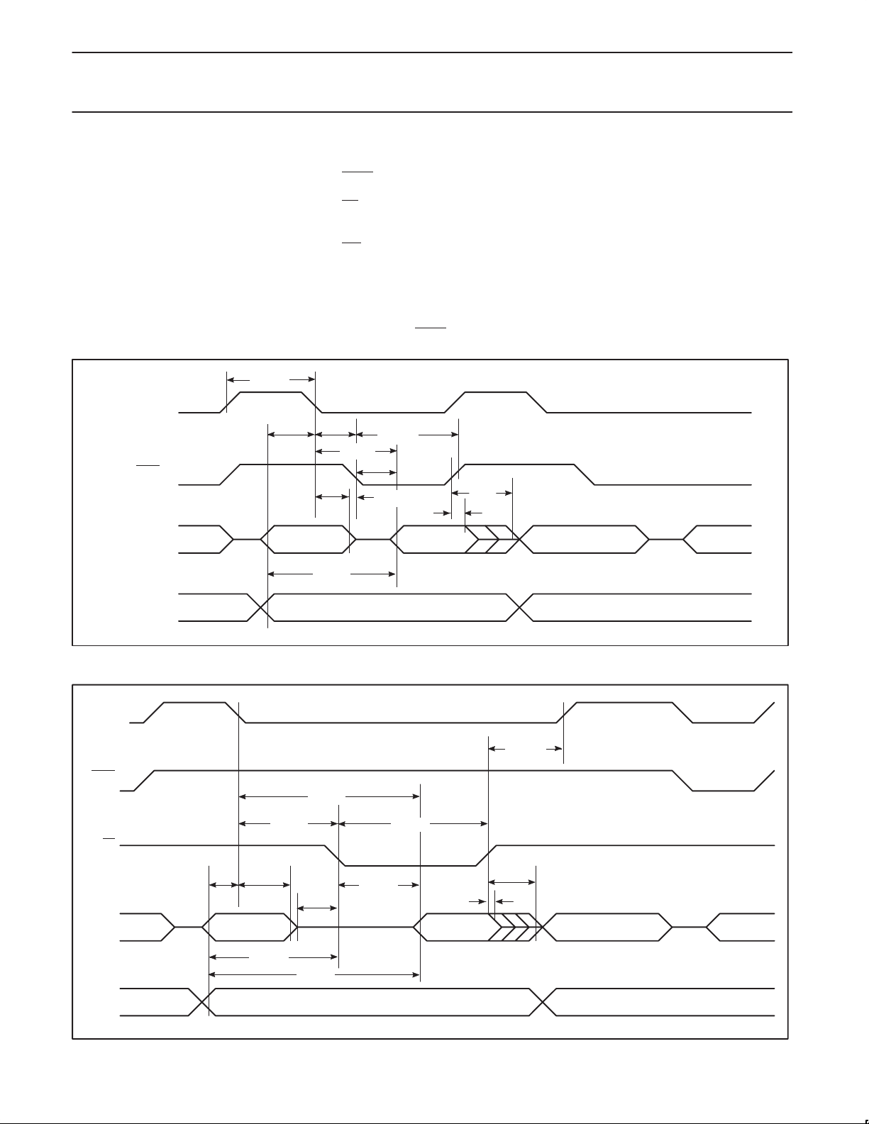
Philips Semiconductors Product specification
80C51 8-bit microcontroller family
8K/256 OTP/ROM/ROMless, 4 comparator, failure detect circuitry, watchdog timer
EXPLANATION OF THE AC SYMBOLS
Each timing symbol has five characters. The
first character is always ‘t’ (= time). The other
characters, depending on their positions,
indicate the name of a signal or the logical
status of that signal. The designations are:
A – Address
C – Clock
D – Input data
H – Logic level high
I – Instruction (program memory contents)
L – Logic level low, or ALE
t
ALE
PSEN
PORT 0
LHLL
P – PSEN
Q – Output data
R–RD
signal
t – Time
V – Valid
W– WR
signal
X – No longer a valid logic level
Z – Float
Examples: t
= Time for address valid to
AVLL
ALE low.
t
=Time for ALE low to
LLPL
PSEN
low.
t
t
AVLL
LLPL
t
LLAX
A0–A7 A0–A7
t
LLIV
t
PLIV
t
PLPH
t
PLAZ
t
PXIX
INSTR IN
t
PXIZ
80C575/83C575/
87C575
ALE
PSEN
PORT 0
PORT 2
RD
PORT 2
t
AVLL
t
LLAX
A0–A7
FROM RI OR DPL
t
AVWL
t
AVIV
A0–A15 A8–A15
Figure 22. External Program Memory Read Cycle
t
WHLH
t
LLDV
t
LLWL
t
RLAZ
t
AVDV
P2.0–P2.7 OR A8–A15 FROM DPF A0–A15 FROM PCH
t
RLDV
t
RLRH
t
RHDZ
t
RHDX
DATA IN A0–A7 FROM PCL INSTR IN
SU00006
1998 May 01
SU00025
Figure 23. External Data Memory Read Cycle
29
Page 30
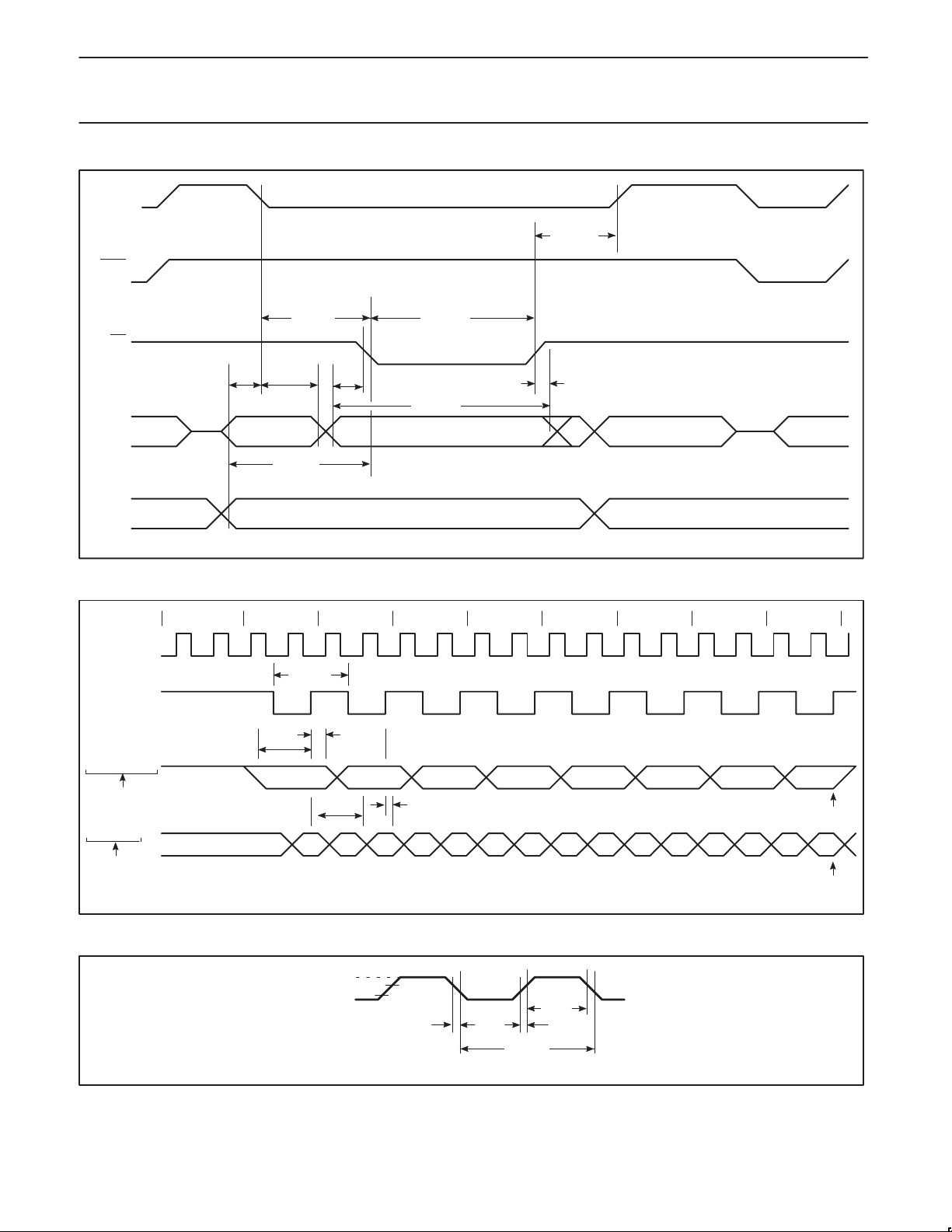
Philips Semiconductors Product specification
80C51 8-bit microcontroller family
8K/256 OTP/ROM/ROMless, 4 comparator, failure detect circuitry, watchdog timer
ALE
t
WHLH
PSEN
t
WLWH
t
WHQX
t
QVWH
DATA OUT A0–A7 FROM PCL INSTR IN
WR
PORT 0
PORT 2
t
AVLL
t
t
LLAX
A0–A7
FROM RI OR DPL
t
AVWL
LLWL
t
QVWX
P2.0–P2.7 OR A8–A15 FROM DPF A0–A15 FROM PCH
80C575/83C575/
87C575
INSTRUCTION
ALE
CLOCK
OUTPUT DATA
WRITE TO SBUF
INPUT DATA
CLEAR RI
SU00026
Figure 24. External Data Memory Write Cycle
012345678
t
XLXL
t
t
QVXH
t
XHDV
VALID VALID VALID VALID VALID VALID VALID VALID
XHQX
1230 4567
t
XHDX
SET TI
SET RI
SU00027
Figure 25. Shift Register Mode Timing
VCC–0.5
0.45V
0.7V
CC
0.2VCC–0.1
t
CHCL
t
CLCX
t
CLCL
t
CHCX
t
CLCH
SU00009
Figure 26. External Clock Drive
1998 May 01
30
Page 31
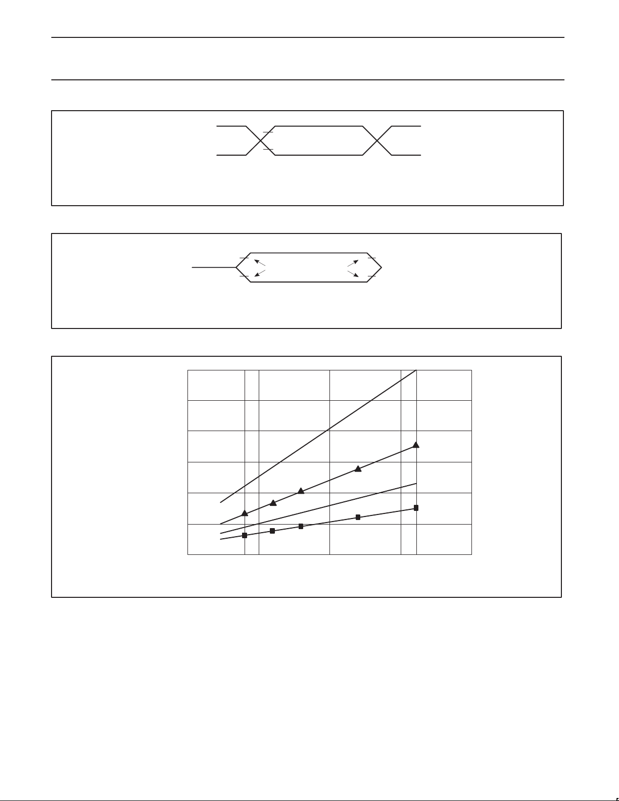
Philips Semiconductors Product specification
80C51 8-bit microcontroller family
8K/256 OTP/ROM/ROMless, 4 comparator, failure detect circuitry, watchdog timer
VCC–0.5
0.45V
NOTE:
AC inputs during testing are driven at VCC –0.5 for a logic ‘1’ and 0.45V for a logic ‘0’.
Timing measurements are made at VIH min for a logic ‘1’ and VIL max for a logic ‘0’.
Figure 27. AC Testing Input/Output
V
+0.1V
V
LOAD
LOAD
NOTE:
For timing purposes, a port is no longer floating when a 100mV change from load voltage occurs,
and begins to float when a 100mV change from the loaded V
V
LOAD
–0.1V
0.2V
+0.9
CC
–0.1
0.2V
CC
TIMING
REFERENCE
POINTS
OH/VOL
Figure 28. Float Waveform
V
V
level occurs. IOH/IOL ≥ ±20mA.
OH
OL
80C575/83C575/
87C575
SU00010
–0.1V
+0.1V
SU00011
30
25
20
15
I
(mA)
CC
10
5
0
045 10 151620
FREQUENCY (MHz)
MAX ACTIVE
TYP ACTIVE
MAX IDLE
TYP IDLE
SU00245
Figure 29. ICC vs. FREQ
Valid only within frequency specifications of the device under test
1998 May 01
31
Page 32
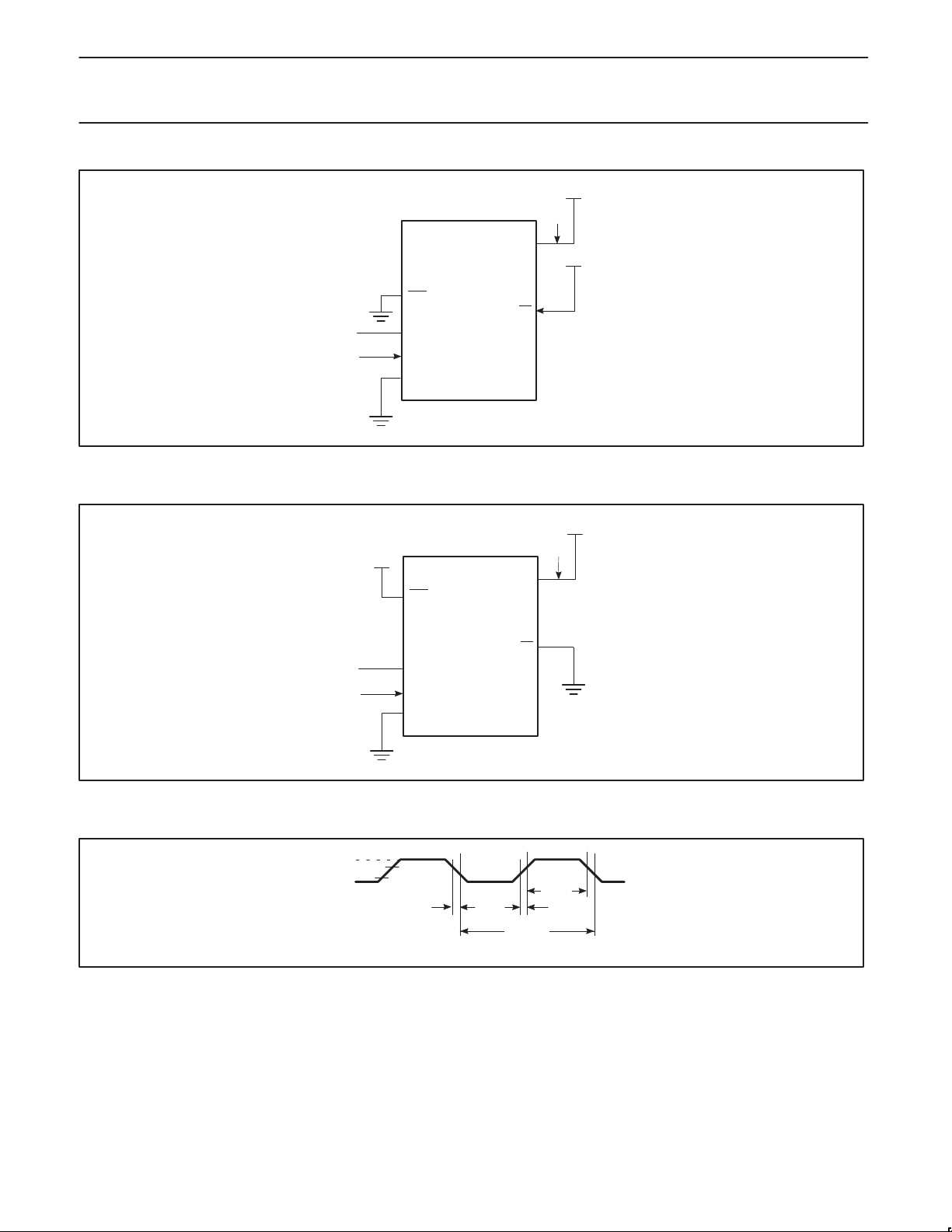
Philips Semiconductors Product specification
80C51 8-bit microcontroller family
8K/256 OTP/ROM/ROMless, 4 comparator, failure detect circuitry, watchdog timer
V
CC
I
CC
V
(NC)
CLOCK SIGNAL
CC
RST
XTAL2
XTAL1
V
SS
EA
Figure 30. ICC Test Condition, Active Mode
All other pins are disconnected
V
CC
V
RST
CC
V
CC
SU00246
V
I
CC
CC
80C575/83C575/
87C575
EA
(NC)
CLOCK SIGNAL
XTAL2
XTAL1
V
SS
SU00247
Figure 31. ICC Test Condition, Idle Mode
All other pins are disconnected
VCC–0.5
0.45V
0.7V
CC
0.2VCC–0.1
t
CHCL
t
CLCX
t
CLCL
t
CHCX
t
CLCH
SU00009
Figure 32. Clock Signal Waveform for ICC Tests in Active and Idle Modes
t
= t
CHCL
= 5ns
CLCH
1998 May 01
32
Page 33
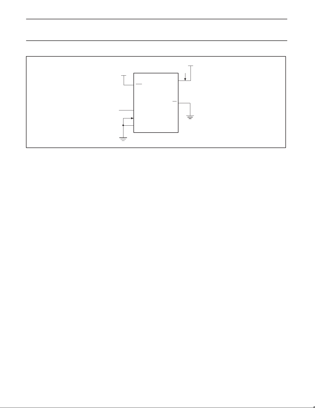
Philips Semiconductors Product specification
80C51 8-bit microcontroller family
8K/256 OTP/ROM/ROMless, 4 comparator, failure detect circuitry, watchdog timer
V
CC
I
V
CC
EA
SU00248
CC
CC
= 2V to 5.5V
V
CC
RST
(NC)
XTAL2
XTAL1
V
SS
Figure 33. ICC Test Condition, Power Down Mode
All other pins are disconnected. V
80C575/83C575/
87C575
1998 May 01
33
Page 34

Philips Semiconductors Product specification
80C51 8-bit microcontroller family
8K/256 OTP/ROM/ROMless, 4 comparator, failure detect circuitry, watchdog timer
EPROM CHARACTERISTICS
To put the 87C575 in the EPROM
programming mode, PSEN must be held high
during power up, then driven low with reset
active. The 87C575 is programmed by using
a modified Quick-Pulse Programming
algorithm. It differs from older methods in the
value used for V
voltage) and in the width and number of the
ALE/PROG
The 87C575 contains two signature bytes
that can be read and used by an EPROM
programming system to identify the device.
The signature bytes identify the device as an
87C575 manufactured by Philips.
Table 3 shows the logic levels for reading the
signature byte, and for programming the
program memory , the encryption table, and
the security bits. The circuit configuration and
waveforms for quick-pulse programming are
shown in Figures 34 and 35. Figure 36 shows
the circuit configuration for normal program
memory verification.
(programming supply
PP
pulses.
Quick-Pulse Programming
The setup for microcontroller quick-pulse
programming is shown in Figure 34. Note that
the 87C575 is running with a 4 to 6MHz
oscillator. The reason the oscillator needs to
be running is that the device is executing
internal address and program data transfers.
The address of the EPROM location to be
programmed is applied to ports 1 and 2, as
shown in Figure 34. The code byte to be
programmed into that location is applied to
port 0. RST, PSEN
specified in Table 3 are held at the ‘Program
Code Data’ levels indicated in Table 3. The
ALE/PROG
in Figure 35.
To program the encryption table, repeat the
25 pulse programming sequence for
addresses 0 through 1FH, using the ‘Pgm
Encryption Table’ levels. Do not forget that
after the encryption table is programmed,
verification cycles will produce only encrypted
data.
To program the security bits, repeat the 25
pulse programming sequence using the ‘Pgm
Security Bit’ levels. After one security bit is
programmed, further programming of the
code memory and encryption table is
disabled. However, the other security bit can
still be programmed.
Note that the EA
to go above the maximum specified V
for any amount of time. Even a narrow glitch
above that voltage can cause permanent
damage to the device. The V
should be well regulated and free of glitches
and overshoot.
and pins of ports 2 and 3
is pulsed low 25 times as shown
/VPP pin must not be allowed
PP
source
PP
level
80C575/83C575/
87C575
Program Verification
If security bit 2 has not been programmed,
the on-chip program memory can be read out
for program verification. The address of the
program memory locations to be read is
applied to ports 1 and 2 as shown in
Figure 36. The other pins are held at the
‘Verify Code Data’ levels indicated in Table 3.
The contents of the address location will be
emitted on port 0. External pull-ups are
required on port 0 for this operation.
If the encryption table has been programmed,
the data presented at port 0 will be the
exclusive NOR of the program byte with one
of the encryption bytes. The user will have to
know the encryption table contents in order to
correctly decode the verification data. The
encryption table itself cannot be read out.
Reading the Signature Bytes
The signature bytes are read by the same
procedure as a normal verification of
locations 030H and 031H, except that P3.6
and P3.7 need to be pulled to a logic low. The
values are:
(030H) = 15H indicates manufactured by
Philips
(B0H) = 97H indicates 87C575
Program/Verify Algorithms
Any algorithm in agreement with the
conditions listed in Table 3, and which
satisfies the timing specifications, is suitable.
Table 3. EPROM Programming Modes
MODE RST PSEN ALE/PROG EA/V
Read signature 0 0 1 1 0 0 0 0
Program code data 0 0 0* V
Verify code data 0 0 1 1 0 0 1 1
Pgm encryption table 0 0 0* V
Pgm security bit 1 0 0 0* V
Pgm security bit 2 0 0 0* V
NOTES:
1. ‘0’ = Valid low for that pin, ‘1’ = valid high for that pin.
= 12.75V ±0.25V.
2. V
PP
3. V
= 5V±10% during programming and verification.
CC
* ALE/PROG
minimum of 10µs.
Trademark phrase of Intel Corporation.
receives 25 programming pulses while VPP is held at 12.75V . Each programming pulse is low for 100 µs (±10µs) and high for a
PP
PP
PP
PP
PP
P2.7 P2.6 P3.7 P3.6
1 0 1 1
1 0 1 0
1 1 1 1
1 1 0 0
1998 May 01
34
Page 35
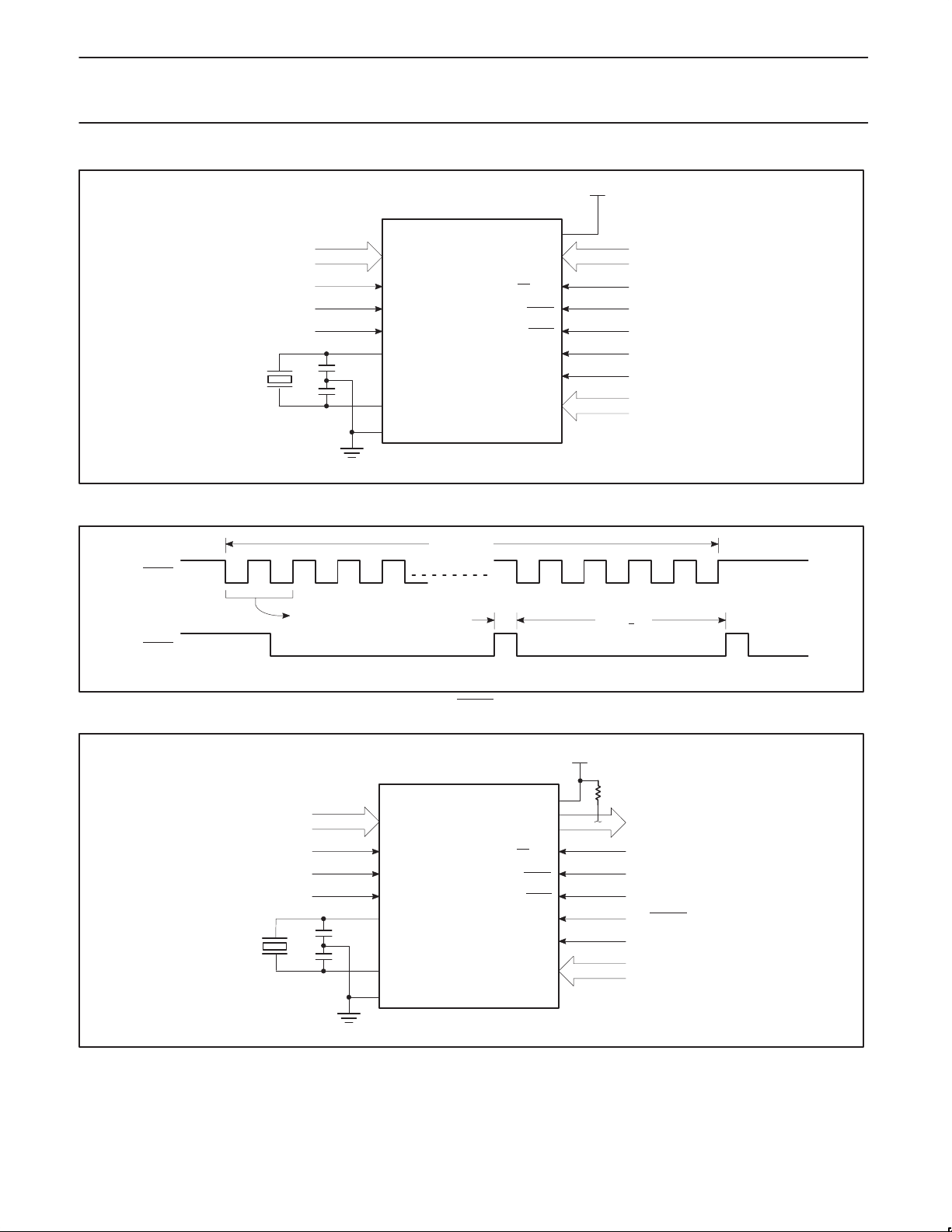
Philips Semiconductors Product specification
80C51 8-bit microcontroller family
8K/256 OTP/ROM/ROMless, 4 comparator, failure detect circuitry, watchdog timer
V
CC
/V
EA
PP
ALE/PROG
PSEN
P2.7
P2.6
P2.0–P2.4
P0
4–6MHz
A0–A7
P1
0
1
1
RST
P3.6
P3.7
XTAL2
XTAL1
V
SS
87C575
Figure 34. Programming Configuration
80C575/83C575/
87C575
+5V
PGM DATA
+12.75V
25 100µs PULSES TO GROUND
0
1
0
A8–A12
SU00249
ALE/PROG:
ALE/PROG:
1
0
4–6MHz
1
0
A0–A7
25 PULSES
100µs+1010µs MIN
SU00018
Figure 35. PROG Waveform
+5V
V
CC
EA
/V
PP
ALE/PROG
PSEN
P2.7
P2.6
P2.0–P2.4
P0
P1
0
1
1
RST
P3.6
P3.7
XTAL2
XTAL1
87C575
PGM DATA
1
1
0
0 ENABLE
0
A8–A12
1998 May 01
V
SS
Figure 36. Program Verification
35
SU00250
Page 36
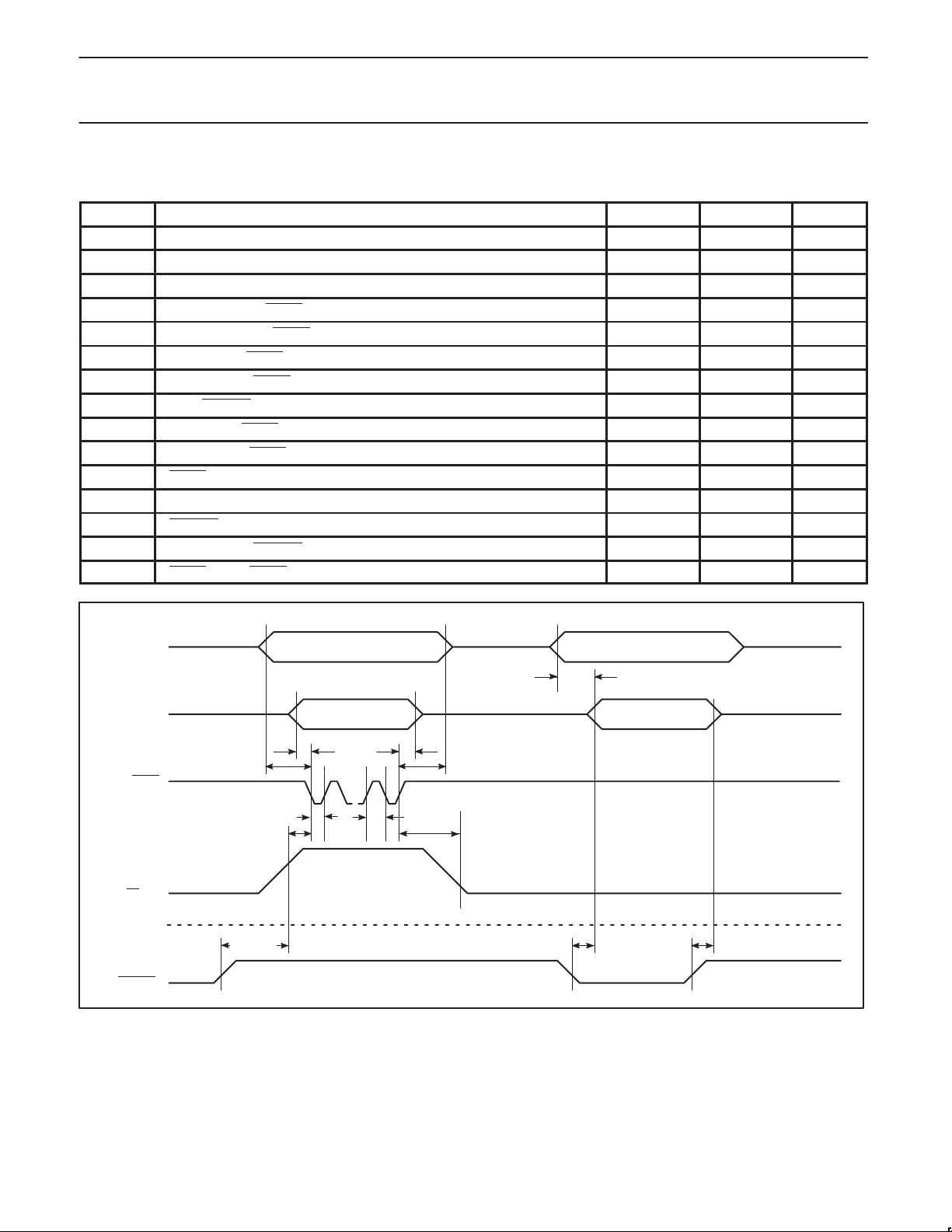
Philips Semiconductors Product specification
80C51 8-bit microcontroller family
8K/256 OTP/ROM/ROMless, 4 comparator, failure detect circuitry, watchdog timer
EPROM PROGRAMMING AND VERIFICATION CHARACTERISTICS
T
= 21°C to +27°C, VCC = 5V±10%, VSS = 0V (See Figure 37)
amb
SYMBOL
V
PP
I
PP
1/t
CLCL
t
AVGL
t
GHAX
t
DVGL
t
GHDX
t
EHSH
t
SHGL
t
GHSL
t
GLGH
t
AVQV
t
ELQZ
t
EHQZ
t
GHGL
Programming supply voltage 12.5 13.0 V
Programming supply current 50 mA
Oscillator frequency 4 6 MHz
Address setup to PROG low 48t
Address hold after PROG 48t
Data setup to PROG low 48t
Data hold after PROG 48t
P2.7 (ENABLE) high to V
VPP setup to PROG low 10 µs
VPP hold after PROG 10 µs
PROG width 90 110 µs
Address to data valid 48t
ENABLE low to data valid 48t
Data float after ENABLE 0 48t
PROG high to PROG low 10 µs
PARAMETER MIN MAX UNIT
PP
48t
80C575/83C575/
87C575
CLCL
CLCL
CLCL
CLCL
CLCL
CLCL
CLCL
CLCL
PROGRAMMING* VERIFICATION*
P1.0–P1.7
P2.0–P2.4
PORT 0
t
DVGL
t
ALE/PROG
EA/V
PP
P2.7
ENABLE
* FOR PROGRAMMING VERIFICATION SEE FIGURE 34.
FOR VERIFICATION CONDITIONS SEE FIGURE 36.
AVGL
t
EHSH
t
GLGH
t
SHGL
ADDRESS ADDRESS
t
AVQV
DATA IN DATA OUT
t
GHDX
t
GHAX
t
GHGL
LOGIC 0
t
GHSL
LOGIC 1 LOGIC 1
t
ELQV
Figure 37. EPROM Programming and Verification
t
EHQZ
SU00020
1998 May 01
36
Page 37
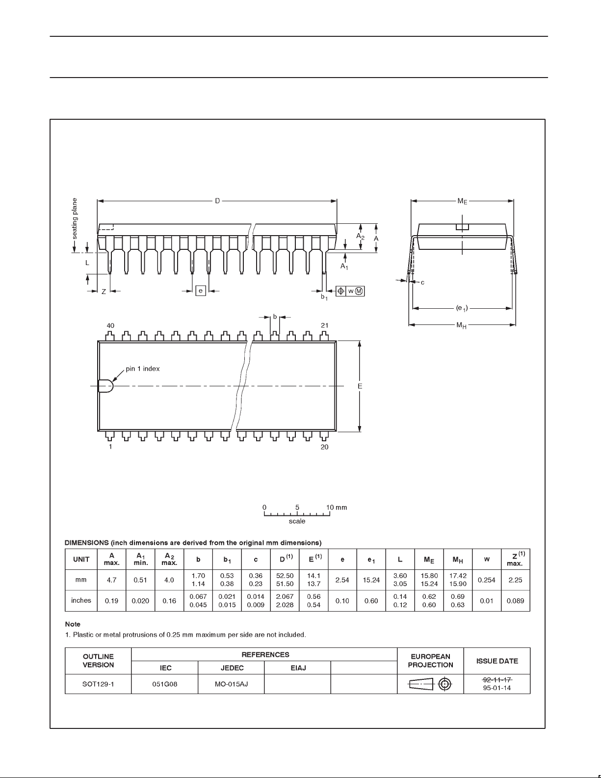
Philips Semiconductors Product specification
80C51 8-bit microcontroller family
8K/256 OTP/ROM/ROMless, 4 comparator, failure detect circuitry, watchdog timer
DIP40: plastic dual in-line package; 40 leads (600 mil) SOT129-1
80C575/83C575/
87C575
1998 May 01
37
Page 38
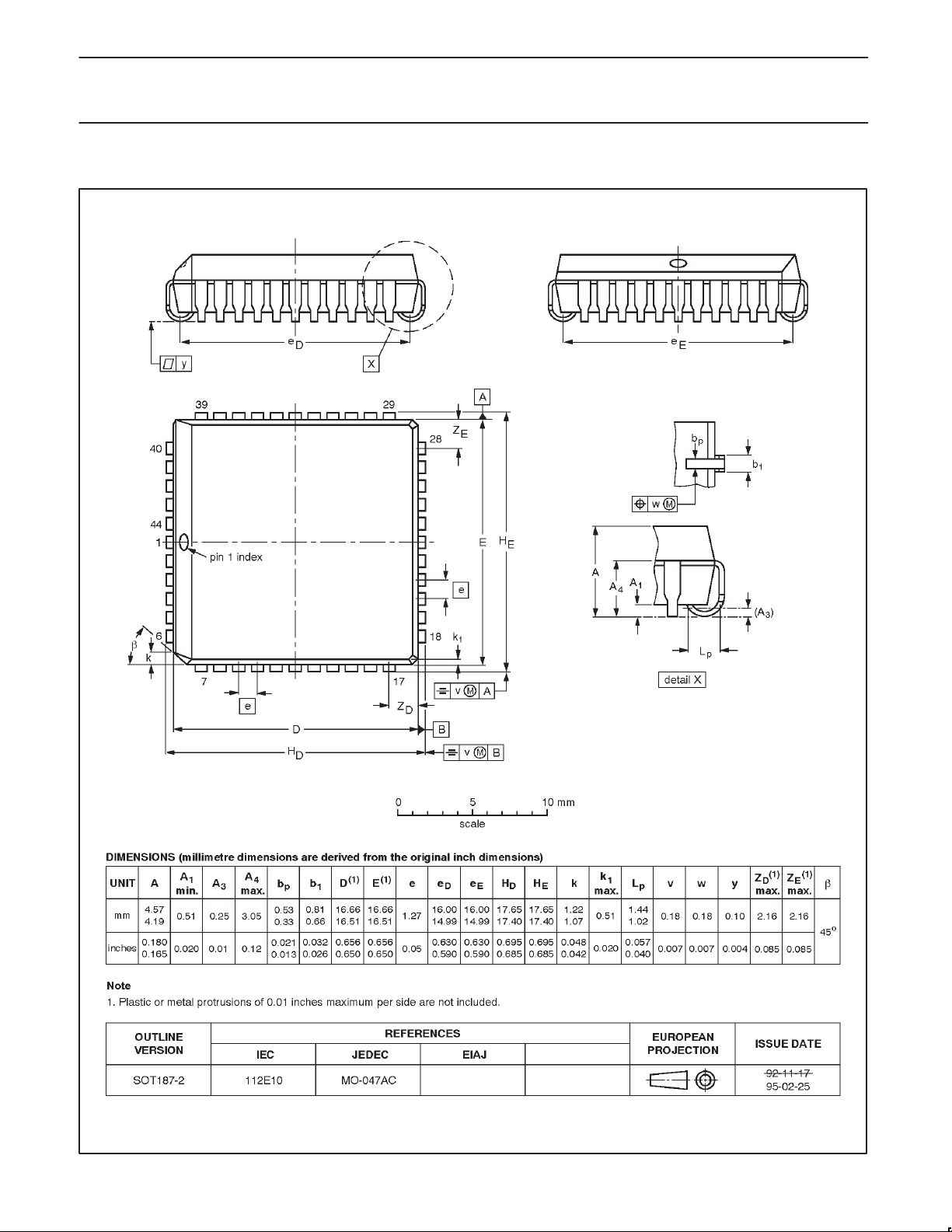
Philips Semiconductors Product specification
80C51 8-bit microcontroller family
8K/256 OTP/ROM/ROMless, 4 comparator, failure detect circuitry, watchdog timer
PLCC44: plastic leaded chip carrier; 44 leads SOT187-2
80C575/83C575/
87C575
1998 May 01
38
Page 39
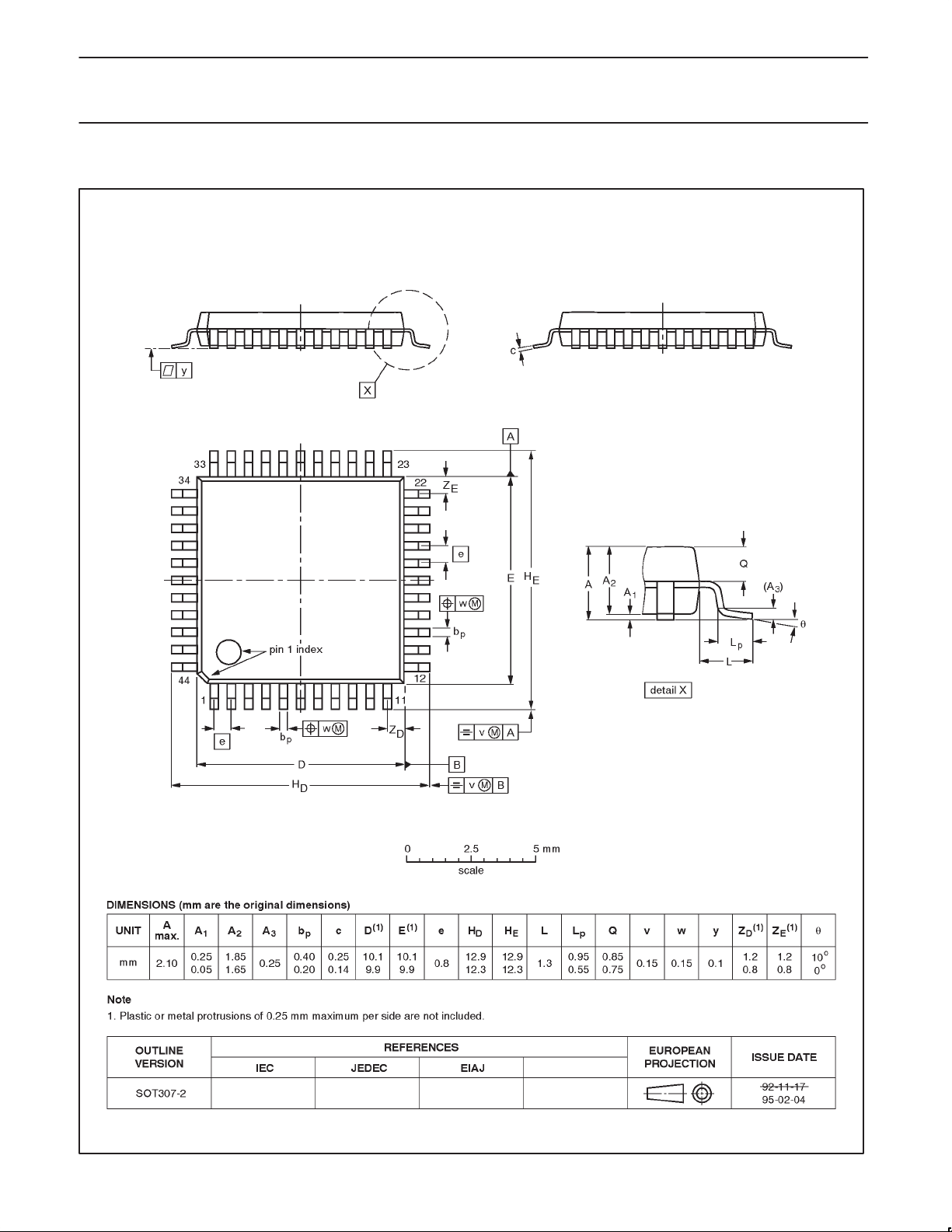
Philips Semiconductors Product specification
80C51 8-bit microcontroller family
8K/256 OTP/ROM/ROMless, 4 comparator, failure detect circuitry, watchdog timer
QFP44: plastic quad flat package; 44 leads (lead length 1.3 mm); body 10 x 10 x 1.75 mm SOT307-2
80C575/83C575/
87C575
1998 May 01
39
Page 40

Philips Semiconductors Product specification
80C51 8-bit microcontroller family
8K/256 OTP/ROM/ROMless, 4 comparator, failure detect circuitry, watchdog timer
Data sheet status
Data sheet
status
Objective
specification
Preliminary
specification
Product
specification
Product
status
Development
Qualification
Production
Definition
This data sheet contains the design target or goal specifications for product development.
Specification may change in any manner without notice.
This data sheet contains preliminary data, and supplementary data will be published at a later date.
Philips Semiconductors reserves the right to make chages at any time without notice in order to
improve design and supply the best possible product.
This data sheet contains final specifications. Philips Semiconductors reserves the right to make
changes at any time without notice in order to improve design and supply the best possible product.
[1]
80C575/83C575/
87C575
[1] Please consult the most recently issued datasheet before initiating or completing a design.
Definitions
Short-form specification — The data in a short-form specification is extracted from a full data sheet with the same type number and title. For
detailed information see the relevant data sheet or data handbook.
Limiting values definition — Limiting values given are in accordance with the Absolute Maximum Rating System (IEC 134). Stress above one
or more of the limiting values may cause permanent damage to the device. These are stress ratings only and operation of the device at these or
at any other conditions above those given in the Characteristics sections of the specification is not implied. Exposure to limiting values for extended
periods may affect device reliability.
Application information — Applications that are described herein for any of these products are for illustrative purposes only. Philips
Semiconductors make no representation or warranty that such applications will be suitable for the specified use without further testing or
modification.
Disclaimers
Life support — These products are not designed for use in life support appliances, devices or systems where malfunction of these products can
reasonably be expected to result in personal injury . Philips Semiconductors customers using or selling these products for use in such applications
do so at their own risk and agree to fully indemnify Philips Semiconductors for any damages resulting from such application.
Right to make changes — Philips Semiconductors reserves the right to make changes, without notice, in the products, including circuits, standard
cells, and/or software, described or contained herein in order to improve design and/or performance. Philips Semiconductors assumes no
responsibility or liability for the use of any of these products, conveys no license or title under any patent, copyright, or mask work right to these
products, and makes no representations or warranties that these products are free from patent, copyright, or mask work right infringement, unless
otherwise specified.
Philips Semiconductors
811 East Arques Avenue
P.O. Box 3409
Sunnyvale, California 94088–3409
Telephone 800-234-7381
Copyright Philips Electronics North America Corporation 1998
All rights reserved. Printed in U.S.A.
Date of release: 05-98
Document order number: 9397 750 03854
1998 May 01
40
 Loading...