

Page 1

INTEGRATED CIRCUITS
80C550/83C550/87C550
80C51 8-bit microcontroller family
4K/128 OTP/ROM/ROMless, 8 channel 8 bit A/D,
watchdog timer
Product specification
Supersedes data of 1998 Jan 19
IC20 Data Handbook
1998 May 01
Page 2

Philips Semiconductors Product specification
80C51 8-bit microcontroller family
4K/128 OTP/ROM/ROMless, 8 channel 8 bit A/D, watchdog timer
DESCRIPTION
The Philips 8XC550 is a high-performance microcontroller fabricated
with Philips high-density CMOS technology. This Philips CMOS
technology combines the high speed and density characteristics of
HMOS with the low power attributes of CMOS. Philips epitaxial
substrate minimizes latch-up sensitivity . The CMOS 8XC550 has the
same instruction set as the 80C51.
The 8XC550 contains a 4k × 8 EPROM (87C550)/ROM
(83C550)/ROMless (80C550 has no program memory on-chip), a
128 × 8 RAM, 8 channels of 8-bit A/D, four 8-bit ports (port 1 is input
only), a watchdog timer, two 16-bit counter/timers, a seven-source,
two-priority level nested interrupt structure, a serial I/O port for either
multi-processor communications, I/O expansion or full duplex UART,
and an on-chip oscillator and clock circuits.
In addition, the 8XC550 has two software selectable modes of
power reduction—idle mode and power-down mode. The idle mode
freezes the CPU while allowing the RAM, timers, serial port, and
interrupt system to continue functioning. The power-down mode
saves the RAM contents but freezes the oscillator, causing all other
chip functions to be inoperative.
FEA TURES
•80C51 based architecture
– 4k × 8 EPROM (87C550)/ROM (83C550)
– 128 × 8 RAM
– Eight channels of 8-bit A/D
– Two 16-bit counter/timers
– Watchdog timer
– Full duplex serial channel
– Boolean processor
•Memory addressing capability
– 64k ROM and 64k RAM
•Power control modes:
– Idle mode
– Power-down mode
•CMOS and TTL compatible
•One speed range at V
– 3.5 to 16MHz
•Extended temperature ranges
•OTP package available
80C550/83C550/87C550
= 5V ±10%
CC
ORDERING INFORMATION
TEMPERATURE RANGE °C
ROMless ROM EPROM
P80C550EBP N P83C550EBP N P87C550EBP N OTP 0 to +70, Plastic Dual In-Line Package 3.5 to 16 SOT129-1
P80C550EBA A P83C550EBA A P87C550EBA A OTP 0 to +70, Plastic Leaded Chip Carrier 3.5 to 16 SOT187-2
P80C550EFA A P83C550EFA A P87C550EFA A OTP –40 to +85, Plastic Leaded Chip Carrier 3.5 to 16 SOT187-2
NOTES:
1. OTP = One Time Programmable EPROM.
AND PACKAGE
1
FREQ
MHz
DRAWING
NUMBER
1998 May 01 853-1568 19329
2
Page 3

Philips Semiconductors Product specification
80C51 8-bit microcontroller family
4K/128 OTP/ROM/ROMless, 8 channel 8 bit A/D, watchdog timer
BLOCK DIAGRAM
P0.0–P0.7 P2.0–P2.7
PORT 0
DRIVERS
V
CC
V
SS
RAM ADDR
REGISTER
B
REGISTER
RAM
ACC
TMP2
PORT 0
LATCH
TMP1
PORT 2
DRIVERS
PORT 2
LATCH
80C550/83C550/87C550
ROM/EPROM
STACK
POINTER
PROGRAM
ADDRESS
REGISTER
PSEN
ALE/PROG
EA/V
PP
RST
TIMING
AND
CONTROL
OSCILLATOR
XTAL1 XTAL2
INSTRUCTION
PD
REGISTER
PSW
PORT 1
LATCH
PORT 1
DRIVERS
P1.0–P1.7
ALU
PCON SCON TMOD TCON
TH0 TL0 TH1
TL1
SBUF IE IP
INTERRUPT, SERIAL
PORT AND TIMER BLOCKS
PORT 3
LATCH
PORT 3
DRIVERS
P3.0–P3.7
BUFFER
PC
INCRE-
MENTER
PROGRAM
COUNTER
DPTR
SU00005
1998 May 01
3
Page 4
Philips Semiconductors Product specification
80C51 8-bit microcontroller family
4K/128 OTP/ROM/ROMless, 8 channel 8 bit A/D, watchdog timer
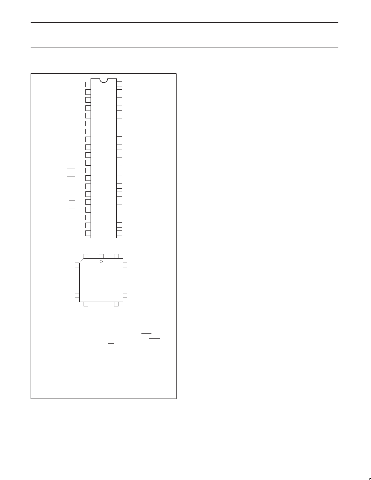
PIN CONFIGURATIONS
40
AVCC/Vref+
/Vref–
AV
SS
P1.0/ADC0
P1.1/ADC1
P1.2/ADC2
P1.3/ADC3
P1.4/ADC4
P1.5/ADC5
RST
RxD/P3.0
TxD/P3.1
INT0
/P3.2
INT1
/P3.3
T0/P3.4
T1/P3.5
WR
/P3.6
RD
/P3.7
XTAL2
XTAL1
V
1
2
3
4
5
6
7
8
9
PLASTIC
DUAL
10
IN-LINE
PACKAGE
11
12
13
14
15
16
17
18
19
20
SS
V
39
P0.0/AD0
38
P0.1/AD1
37
P0.2/AD2
36
P0.3/AD3
35
P0.4/AD4
34
P0.5/AD5
33
P0.6/AD6
32
P0.7/AD7
31
EA/V
30
ALE/PROG
29
PSEN
28
P2.7/A15
27
P2.6/A14
26
P2.5/A13
25
P2.4/A12
24
P2.3/A11
23
P2.2/A10
22
P2.1/A9
21
P2.0/A8
CC
PP
80C550/83C550/87C550
17
Pin Function
1AV
CC
2 Vref+
3 Vref–
4AV
SS
5 P1.0/ADC0
6 P1.1/ADC1
7 P1.2/ADC2
8 P1.3/ADC3
9 P1.4/ADC4
10 P1.5/ADC5
11 P1.6/ADC6
12 P1.7/ADC7
13 RST
14 P3.0/RxD
15 P3.1/TxD
6140
7
PLASTIC
LEADED
CHIP CARRIER
18 28
Pin Function
16 P3.2/INT0
17 P3.3/INT1
18 P3.4/T0
19 P3.5/T1
20 P3.6/WR
21 P3.7/RD
22 XTAL2
23 XTAL1
24 V
25 P2.0/A8
26 P2.1/A9
27 P2.2/A10
28 P2.3/A11
29 P2.4/A12
30 P2.5/A13
39
29
Pin Function
31 P2.6/A14
32 P2.7/A15
33 PSEN
34 ALE/PROG
35 EA/V
36 P0.7/AD7
37 P0.6/AD6
38 P0.5/AD5
SS
39 P0.4/AD4
40 P0.3/AD3
41 P0.2/AD2
42 P0.1/AD1
43 P0.0/AD0
44 V
PP
CC
SU00196
1998 May 01
4
Page 5

Philips Semiconductors Product specification
80C51 8-bit microcontroller family
80C550/83C550/87C550
4K/128 OTP/ROM/ROMless, 8 channel 8 bit A/D, watchdog timer
PIN DESCRIPTION
PIN NO.
MNEMONIC DIP LCC TYPE NAME AND FUNCTION
V
SS
V
CC
AV
CC
AV
SS
Vref+
Vref–
P0.0–0.7 39–32 43–36 I/O Port 0: Port 0 is an open-drain, bidirectional I/O port. Port 0 pins that have 1s written to them float
P1.0–P1.7 3–8 5–12 I Port 1: Port 1 is an 8-bit input only port (6-bit in the DIP package; bits P1.6 and P1.7 are not
ADC0–ADC7 3–8 5–12 ADCx: Inputs to the analog multiplexer input of the 8-bit A/D. There are only six A/D inputs in the
P2.0–P2.7 21–28 25–32 I/O Port 2: Port 2 is an 8-bit bidirectional I/O port with internal pull-ups. Port 2 pins that have 1s written
P3.0–P3.7 10–17 14–21 I/O Port 3: Port 3 is an 8-bit bidirectional I/O port with internal pull-ups. Port 3 pins that have 1s written
RST 9 13 I Reset: A high on this pin for two machine cycles while the oscillator is running, resets the device.
ALE/PROG 30 34 I/O Address Latch Enable/Program Pulse: Output pulse for latching the low byte of the address
PSEN 29 33 O Program Store Enable: The read strobe to external program memory. When the device is
EA/V
PP
XTAL1 19 23 I Crystal 1: Input to the inverting oscillator amplifier and input to the internal clock generator circuits.
XTAL2 18 22 O Crystal 2: Output from the inverting oscillator amplifier.
20 24 I Ground: 0V reference.
40 44 I Power Supply: This is the power supply voltage for normal, idle, and power-down operation.
1 1 I Analog Power Supply: Analog supply voltage.
2 4 I Analog Ground: Analog 0V reference.
2
3
IIVref: A/D converter reference level inputs. Note that these references are combined with AVCC and
in the 40-pin DIP package.
AV
SS
and can be used as high-impedance inputs. Port 0 is also the multiplexed low-order address and
data bus during accesses to external program and data memory. In this application, it uses strong
internal pull-ups when emitting 1s. Port 0 also outputs the code bytes during program verification in
the S87C550. External pull-ups are required during program verification.
implemented). Port 1 digital input can be read out any time.
DIP package.
to them are pulled high by the internal pull-ups and can be used as inputs. As inputs, port 2 pins that
are externally being pulled low will source current because of the internal pull-ups. (See DC
Electrical Characteristics: I
program memory and during accesses to external data memory that use 16-bit addresses (MOVX
). Port 2 emits the high-order address byte during fetches from external
IL
@DPTR). In this application, it uses strong internal pull-ups when emitting 1s. During accesses to
external data memory that use 8-bit addresses (MOV @Ri), port 2 emits the contents of the P2
special function register.
to them are pulled high by the internal pull-ups and can be used as inputs. As inputs, port 3 pins that
are externally being pulled low will source current because of the pull-ups. (See DC Electrical
Characteristics: I
). Port 3 also serves the special features of the SC80C51 family, as listed below:
IL
10 14 I RxD (P3.0): Serial input port
11 15 O TxD (P3.1): Serial output port
12 16 I INT0 (P3.2): External interrupt
13 17 I INT1 (P3.3): External interrupt
14 18 I T0 (P3.4): Timer 0 external input
15 19 I T1 (P3.5): Timer 1 external input
16 20 O WR (P3.6): External data memory write strobe
17 21 O RD (P3.7): External data memory read strobe
An internal diffused resistor to V
.
V
CC
permits a power-on reset using only an external capacitor to
SS
during an access to external memory. In normal operation, ALE is emitted at a constant rate of 1/6
the oscillator frequency , and can be used for external timing or clocking. Note that one ALE pulse is
skipped during each access to external data memory. This pin is also the program pulse input
(PROG
) during EPROM programming.
executing code from the external program memory, PSEN
except that two PSEN
activations are skipped during each access to external data memory. PSEN
is activated twice each machine cycle,
is not activated during fetches from internal program memory.
31 35 I External Access Enable/Programming Supply Voltage: EA must be externally held low to enable
the device to fetch code from external program memory locations 0000H to 0FFFH. If EA
is held
high, the device executes from internal program memory unless the program counter contains an
address greater than 0FFFH. For the 80C550 ROMless part, EA
operate properly . This pin also receives the 12.75V programming supply voltage (V
EPROM programming.
must be held low for the part to
) during
PP
1998 May 01
5
Page 6
Philips Semiconductors Product specification
80C51 8-bit microcontroller family
80C550/83C550/87C550
4K/128 OTP/ROM/ROMless, 8 channel 8 bit A/D, watchdog timer
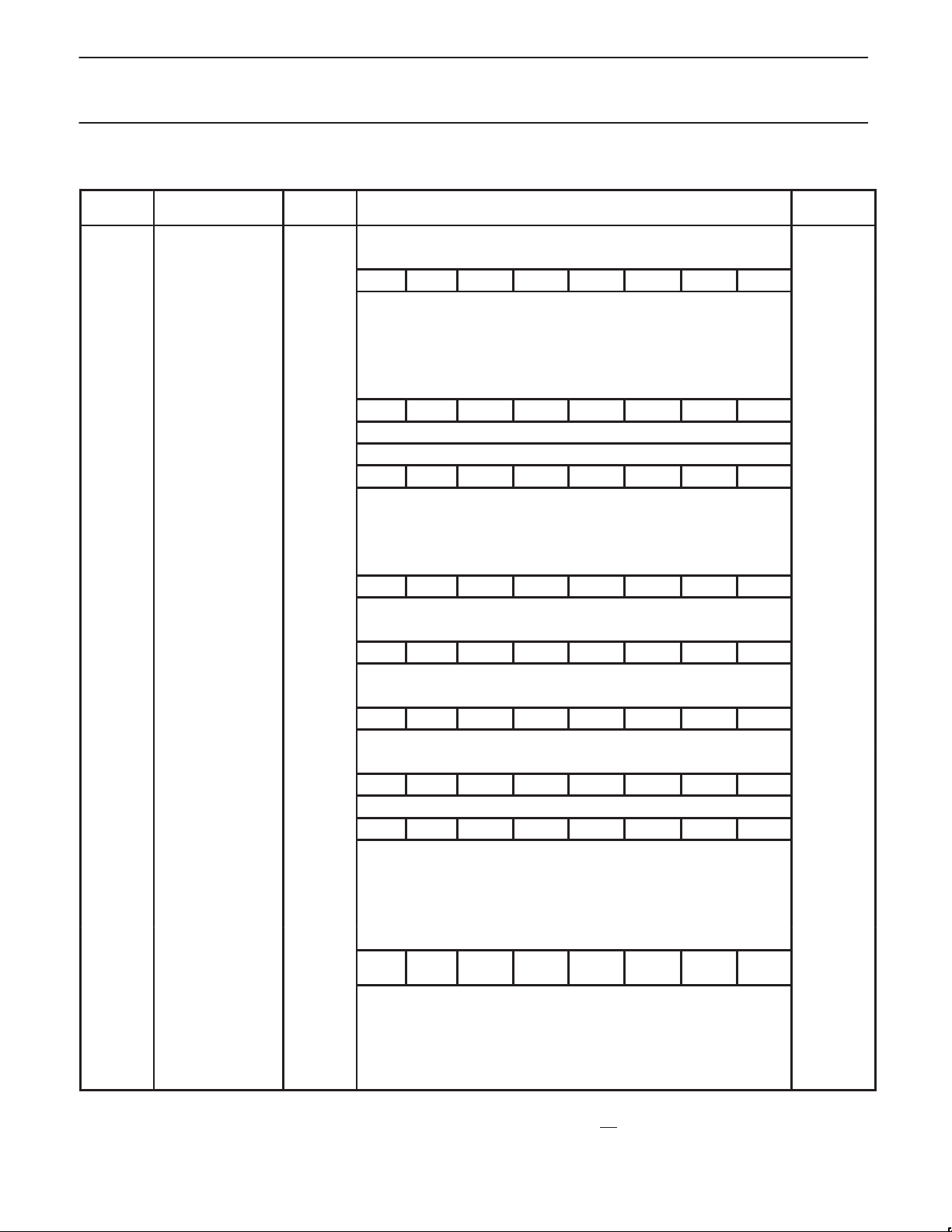
Table 1. 8XC550 Special Function Registers
SYMBOL DESCRIPTION
ACC* Accumulator E0H E7 E6 E5 E4 E3 E2 E1 E0 00H
ADAT# A/D result C6H xxH
ADCON# A/D control C5H – – – ADCI ADCS AADR2 AADR1 AADR0 xxx00000B
B* B register F0H F7 F6 F5 F4 F3 F2 F1 F0 00H
DPTR:
DPH
DPL
IP*# Interrupt priority B8H – PWD PAD PS PT1 PX1 PT0 PX0 x0000000B
IE*# Interrupt enable A8H EA EWD EAD ES ET1 EX1 ET0 EX0 00H
P0* Port 0 80H 87 86 85 84 83 82 81 80 FFH
P1* Port 1 90H 97 96 95 94 93 92 91 90 FFH
P2* Port 2 A0H A7 A6 A5 A4 A3 A2 A1 A0 FFH
P3* Port 3 B0H B7 B6 B5 B4 B3 B2 B1 B 0 FFH
PCON# Power control 87H SMOD SIDL – – GF1 GF0 PD IDL 00xx0000B
Data pointer
(2 bytes):
High byte
Low byte
DIRECT
ADDRESS
83H
82H
BIT ADDRESS, SYMBOL, OR ALTERNATIVE PORT FUNCTION
MSB LSB
BF BE BD BC BB BA B9 B8
AF AE AD AC AB AA A9 A8
RESET
VALUE
00H
00H
D7 D6 D5 D4 D3 D2 D1 D0
PSW* Program status word D0H CY AC F0 RS1 RS0 OV – P 00H
SBUF Serial data buffer 99H xxH
9F 9E 9D 9C 9B 9A 99 98
SCON* Serial port control 98H SM0 SM1 SM2 REN TB8 RB8 TI RI 00H
SP Stack pointer 81H 07H
8F 8E 8D 8C 8B 8A 89 88 00H
TCON* Timer counter/control 88H TF1 TR1 TF0 TR0 IE1 IT1 IE0 IT0 00H
TMOD Timer/counter mode 89H GATE C/T M1 M0 GATE C/T M1 M0 00H
TH0 Timer 0 high byte 8CH 00H
TH1 Timer 1 high byte 8DH 00H
TL0 Timer 0 low byte 8AH 00H
TL1 Timer 1 low byte 8BH 00H
C7 C6 C5 C4 C3 C2 C1 C0
WDCON*# Watchdog timer
control
WDL# Watchdog timer
reload
WFEED1# Watchdog timer
feed 1
WFEED2# Watchdog timer
feed 2
* SFRs are bit addressable.
# SFRs are modified from or added to the 80C51 SFRs.
**This value is not valid for a masked ROM part (83C550) when running from internal memory (EA
C0H PRE2 PRE1 PRE0 – –
C1H FFH**
C2H xxH
C3H xxH
WDRUN WDTOF
= 1). See data sheet for details.
WDMOD
000xx000B**
1998 May 01
6
Page 7

Philips Semiconductors Product specification
80C51 8-bit microcontroller family
4K/128 OTP/ROM/ROMless, 8 channel 8 bit A/D, watchdog timer
SMOD SIDL X
BIT SYMBOL FUNCTION
PCON.7 SMOD Double baud rate
PCON.6 SIDL Serial port idle
PCON.5 X Reserved for future use
PCON.4 X Reserved for future use
PCON.3 GF1 General purpose flag bit
PCON.2 GF0 General purpose flag bit
PCON.1 PD Power down bit
PCON.0 IDL Idle mode bit
NOTE:
The PCON register is at SFR byte address 87H. Its contents following a reset are 00XX0000.
Figure 1. Power Control Register (PCON)
X GF1 GF0 PD IDL
80C550/83C550/87C550
LSBMSB
SU00197
LSBMSB
XXX
INPUT CHANNEL SELECTION
ADDR2 ADDR1 ADDR0 INPUT PIN
0 0 0 ADC0
0 0 1 ADC1
0 1 0 ADC2
0 1 1 ADC3
1 0 0 ADC4
1 0 1 ADC5
1 1 0 ADC6
1 1 1 ADC7
BIT SYMBOL FUNCTION
ADCON.7 — Not used
ADCON.6 — Not used
ADCON.5 — Not used
ADCON.4 ADCI ADC Interrupt flag.
This flag is set when an ADC conversion result is ready to be read. An interrupt is invoked if the
A/D interrupt is enabled. The flag must be cleared by software. It cannot be set by software.
ADCON.3 ADCS ADC Start and Status.
Setting this flag starts an A/D conversion. The ADC logic insures that this signal is high while the
ADC is busy. On completion of the conversion, ADCS is reset at the same time the interrupt flag
ADCI is set. ADCS cannot be reset by software.
ADCON.2 ADDR2 Analog Input Select 2
ADCON.1 ADDR1 Analog Input Select 1
ADCON.0 ADDR0 Analog Input Select 0
ADCI ADCS AADR2 AADR1 AADR0
SU00198
1998 May 01
Figure 2. A/D Control Register (ADCON)
7
Page 8

Philips Semiconductors Product specification
80C51 8-bit microcontroller family
4K/128 OTP/ROM/ROMless, 8 channel 8 bit A/D, watchdog timer
A/D CONVERTER
The analog input circuitry consists of an 8-input analog multiplexer
and an analog-to-digital converter with 8-bit resolution. In the LCC
package, the analog reference voltage and analog power supplies
are connected via separate input pins; in the DIP package, Vref+ is
combined with AV
inputs are alternate functions to port 1, which is an input only port.
Digital input to port 1 can be read any time during an A/D
conversion. Care should be exercised in mixing analog and digital
signals on port 1, because cross talk from the digital input signals
can degrade the A/D conversion accuracy of the analog input. An
A/D conversion requires 40 machine cycles.
The A/D converter is controlled by the ADCON special function
register. The input channel to be converted is selected by the analog
multiplexer by setting ADCON register bits, ADDR2–ADDR0 (see
Figure 2). These bits can only be changed when ADCI and ADCS
are both low.
The completion of the 8-bit ADC conversion is flagged by ADCI in
the ADCON register and the result is stored in the special function
register ADAT.
An ADC conversion in progress is unaffected by a software ADC
start. The result of a completed conversion remains unaffected
provided ADCI remains at a logic 1. While ADCS is a logic 1 or
ADCI is a logic 1, a new ADC START will be blocked and
consequently lost. An A/D conversion in progress will be aborted
when the idle or power-down mode is entered. The result of a
completed conversion (ADCI = logic 1) remains unaffected when
entering the idle mode, but will be lost if power-down mode is
entered. See Figure 3 for the A/D input equivalent circuit.
The analog input pins ADC0-ADC7 may still be used as digital
inputs. The analog input channel that is selected by the
ADDR2-ADDR0 bits in ADCON cannot be used as a digital input.
Reading the selected A/D channel as a digital input will always
return a 1. The unselected A/D inputs may always be used as digital
inputs.
On RESET the A/D port pins are set to the Digital mode and will
work as a normal port and need no further initialization. To use the
A/D converter a single byte should be written to ADCON which
selects the A/D mux and concurrently sets the ADCS bit to start the
A/D conversion. The 40 machine cycles of the A/D conversion
include time for signal settling after the mux is selected and before
the Sample and Hold procedure is completed.
The circuitry which disables the digital buffer from the port pin is
updated at the start of an A/D conversion by setting the ADCS bit in
ADCON. After powerup, problems will occur the first time that
ADCON is written to if ADCS is not set; in this case, the digital
signal disable registers contain random data and some o the 8 port
pins will have their digital buffers disabled. When read, these
disabled buffers will ignore their input and only return a 1. This
condition will be corrected by writing a 1 to ADCS in ADCON which
starts and A/D conversion.
Thus, there are two operating modes:
1. DIGITAL ONLY - No Analog inputs are used and ADCON is
never written to. In this case pins ADC0-ADC7 are configured as
digital inputs.
2. A/D CONVERTER USED - The input multiplexer select field
must be written to and ADCS must be set in ADCON. This allows
unselected A/D inputs to be used as digital inputs.
and Vref– is combined with AVSS. The analog
CC
ADCON Register
ADCI ADCS Operation
*Not present on 40-pin DIP versions.
Symbol Position Function
ADCI ADCON.4 ADC interrupt flag. This flag is set when an
ADCS ADCON.3 ADC start and status. Setting this bit starts an
AADR2 ADCON.2 Analog input selects.
AADR1 ADCON.1 Binary coded address
AADR0 ADCON.0 selects one of the five analog input port pins of
80C550/83C550/87C550
MSB LSB
X X ADCI SDCS AADR2 AADR1 AADR0
X
0 0 ADC not busy, a conversion can be started.
0 1 ADC busy, start of a new conversion is blocked.
1 0 Conversion completed, start of a new is blocked.
1 1 Not possible.
INPUT CHANNEL SELECTION
ADDR2 ADDR1 ADDR0 INPUT PIN
0
0
0
0
1
1
1
1
0
0
1
1
0
0
1
1
ADC conversion is complete. If IE.5 = 1, an
interrupt is requested when ADCI = 1. The
ADCI flag must be cleared by software after
A/D data is read, before the next conversion
can begin.
A/D conversion. Once set, ADCS remains high
throughout the conversion cycle. On
completion of the conversion, it is reset at the
same time the ADCI interrupt flag is set. ADCS
cannot be reset by software.
P1 to be input to the converter. It can only be
changed when ADCI and ADCS are both l ow.
AADR2 is the most significant bit.
0
1
0
1
0
1
0
1
P1.0
P1.1
P1.2
P1.3
P1.4
P1.5
P1.6*
P1.7*
1998 May 01
8
Page 9
Philips Semiconductors Product specification
80C51 8-bit microcontroller family
4K/128 OTP/ROM/ROMless, 8 channel 8 bit A/D, watchdog timer
Sample A/D Routines
The following routines demonstrate two methods of operating the
A/D converter. The first method uses polling to determine when the
A/D conversion is complete. The second method uses the A/D
interrupt to flag the end of conversion.
The routine ReadAD will start a read of the A/D channel identified by
R7, and wait for the conversion to complete, polling the A/D interrupt
flag. The result is returned in the accumulator.
ReadAD:MOV A,#08h ;Basic A/D start command.
ORL A,R7 ;Add channel # to be read.
MOV ADCON,A; ;Start A/D.
ADLoop: MOV A,ADCON ;Get A/D status.
JNB ACC.4,ADLoop;Wait for ADCI (A/D ;finished).
MOV A,ADAT ;Get conversion result
MOV ADCON,#0 ;Clear ADCI.
RET
The routine StartAD will start a read of the A/D channel identified by
R7 and exit back to the calling program. When the conversion is
complete, the A/D interrupt occurs, calling the A/D interrupt service
routine. The result of the conversion is returned in register R6.
StartAD: MOV A,#08h ;Basic A/D start command.
ADInt: MOV R6,ADAT ;Get conversion result.
80C550/83C550/87C550
ORL A,R7 ;Add channel # to be read.
MOV ADCON,A ;Start A/D.
RET
.
.
.
ORG 2Bh ;A/D interrupt address.
MOV ADCON,#0 ;Clear ADCI.
RETI
I
Sm
N+1
I
N
+
R
S
V
ANALOG
INPUT
Sm
C
S
N+1
N
Multiplexer
Rm
Rm
N+1
N
To Comparator
C
C
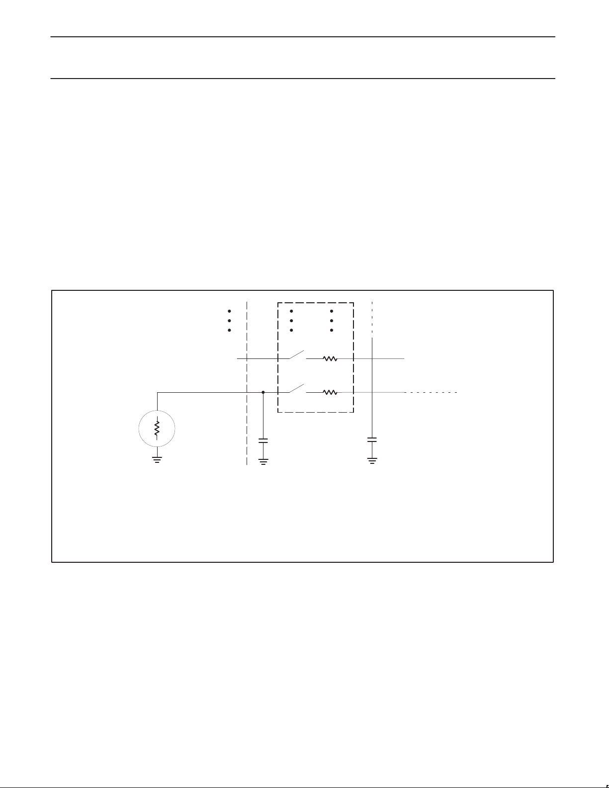
Rm = 0.5 - 3 kΩ
CS + CC = 15pF maximum
RS = Recommended < 9.6 kΩ for 1 LSB @ 12MHz
NOTE:
Because the analog to digital converter has a sampled-data comparator, the input looks capacitive to a source. When a conversion
is initiated, switch Sm closes for 8tcy (8µs @ 12MHz crystal frequency) during which time capacitance Cs + Cc is charged. It should
be noted that the sampling causes the analog input to present a varying load to an analog source.
SU00199
Figure 3. A/D Input: Equivalent Circuit
1998 May 01
9
Page 10

Philips Semiconductors Product specification
80C51 8-bit microcontroller family
4K/128 OTP/ROM/ROMless, 8 channel 8 bit A/D, watchdog timer
A/D CONVERTER P ARAMETER DEFINITIONS
The following definitions are included to clarify some specifications
given and do not represent a complete set of A/D parameter
definitions.
Absolute Accuracy Error
Absolute accuracy error of a given output is the difference between
the theoretical analog input voltage to produce a given output and
the actual analog input voltage required to produce the same code.
Since the same output code is produced by a band of input voltages,
the “required input voltage” is defined as the midpoint of the band of
input voltage that will produce that code. Absolute accuracy error
not specified with a code is the maximum over all codes.
Nonlinearity
If a straight line is drawn between the end points of the actual
converter characteristics such that zero offset and full scale errors
are removed, then non-linearity is the maximum deviation of the
code transitions of the actual characteristics from that of the straight
line so constructed. This is also referred to as relative accuracy and
also integral non-linearity.
Differential Non-Linearity
Differential non-linearity is the maximum difference between the
actual and ideal code widths fo the converter. The code widths are
the differences expressed in LSB between the code transition
points, as the input voltage is varied through the range for the
complete set of codes.
Gain Error
Gain error is the deviation between the ideal and actual analog input
voltage required to cause the final code transition to a full-scale
output code after the offset error has been removed. This may
sometimes be referred to as full scale error.
Offset Error
Offset error is the difference between the actual input voltage that
causes the first code transition and the ideal value to cause the first
code transition. This ideal value is 1/2 LSB above V
ref–
.
Channel to Channel Matching
Channel to channel matching is the maximum difference between
the corresponding code transitions of the actual characteristics
taken from different channels under the same temperature, voltage
and frequency conditions.
Crosstalk
Crosstalk is the measured level of a signal at the output of the
converter resulting from a signal applied to one deselected channel.
T otal Error
Maximum deviation of any step point from a line connecting the ideal
first transition point to the ideal last transition point.
Relative Accuracy
Relative accuracy error is the deviation of the ADC’s actual code
transition points from the ideal code transition points on a straight
line which connects the ideal first code transition point and the final
code transition point, after nullifying offset error and gain error. It is
generally expressed in LSBs or in percent of FSR.
WATCHDOG TIMER
The purpose of the watchdog timer is to reset the microcontroller
within a reasonable amount of time if it enters an erroneous state,
possibly due to a programming error, electrical noise, or RFI. When
enabled, the watchdog circuit will generate a system reset if the user
program fails to “feed” (or reload) the watchdog within a
predetermined amount of time.
The watchdog timer implemented on the 8XC550 has a
programmable interval and can thus be fine tuned to a particular
application. If the watchdog function is not used, the timer may still
be used as a versatile general purpose timer.
The watchdog function consists of a programmable 13-bit prescaler,
and an 8-bit main timer. The main timer is clocked by a tap taken
from one of the top 8 bits of the prescaler. The prescaler is
incremented once every machine cycle, or 1/12 of the oscillator
frequency. Thus, the main counter can be clocked as often as once
every 64 machine cycles or as seldom as once every 8192 machine
cycles.
When clocked, the main counter decrements. If the main watchdog
counter reaches zero, a system reset will occur. To prevent the
watchdog timer from under-flowing, the watchdog must be fed
before it counts down to zero. When the watchdog is fed, the
contents of the WDL register are loaded into the main watchdog
counter and the prescaler is cleared.
WDCON Register
Symbol Position Function
WDCON.7 PRE2 Prescaler select (read/write).
WDCON.6 PRE1 These bits select theprescaler divide ratio
WDCON.5 PRE0 according to the following table:
WDCON.4 – Not used
WDCON.3 – Not used
WDCON.2 WDRUN Run control (read/write).
WDCON.1 WDTOF Timeout flag (read/write).
WDCON.0 WDMOD Mode selection (read/write).
80C550/83C550/87C550
MSB LSB
PRE1 PRE0 X X WDRUN WDTOF WDMOD
PRE2
PRE2
0
0
0
0
1
1
1
1
PRE1 PRE0 DIVISOR (FROM f
0
0
1
1
0
0
1
1
This bit turns the timer on (WDRUN = 1) or off
(WDRUN = 0) if the timer mode has been
selected.
This bit is set when the watchdog timer
underflows. It is cleared by an external reset
and can be cleared by software.
When WDMOD = 1, the watchdog is selected;
when WDMOD = 0, the timer is selected.
Selecting the watchdog mode automatically
disables power-down mode. WDMOD is
cleared by external reset. Once the watchdog
mode is selected, this bit can only be cleared
by writing a 0 to this bit and then performing a
feed operation.
0
1
0
1
0
1
0
1
12 × 64
12 × 64 × 2
12 × 64 × 4
12 × 64 × 8
12 × 64 × 16
12 × 64 × 32
12 × 64 × 64
12 × 64 × 128
OSC
)
1998 May 01
10
Page 11

Philips Semiconductors Product specification
80C51 8-bit microcontroller family
4K/128 OTP/ROM/ROMless, 8 channel 8 bit A/D, watchdog timer
A very specific sequence of events must take place to feed the
watchdog timer; it cannot be fed accidentally by a runaway program.
The following routines demonstrate setting up and feeding the
watchdog timer. These routines apply to all versions of the 8XC550
except the ROM part when running from internal program memory.
This routine sets up and starts the watchdog timer. This is not
necessary for internal ROM operation, because setup of the
watchdog timer on masked ROM parts is accomplished directly via
ROM mask options.
SetWD: MOV WDL,#0FFh ;Set watchdog reload value.
MOV WDCON,#0E5;Set up timer prescaler, mode, and
;run bits.
ACALL FeedWD ;Start watchdog with a feed
;operation.
RET
This routine executes a watchdog timer feed operation, causing the
timer to reload from WDL. Interrupts must be disabled during this
operation due to the fact that the two feed registers must be loaded
on consecutive instruction cycles, or a system reset will occur
immediately.
FeedWD:CLR EA ;This sequence must not be
;interrupted.
MOV WFEED1,#0A5h;First instruction of feed sequence.
MOV WFEED2,#05Ah;Second instruction of feed
;sequence.
SETB EA ;Turn interrupts back on.
RET
An interrupt is available to allow the watchdog timer to be used as a
general purpose timer in applications where the watchdog function is
not needed. The timer operates in the same manner when used as a
general purpose timer except that the timer interrupt is generated on
timer underflow instead of a chip reset. Refer to the 87C550 data
sheet for additional information on watchdog timer operation.
Programming the Watchdog Timer
Both the EPROM and ROM devices have a set of SFRs for holding
the watchdog autoload values and the control bits. The watchdog
time-out flag is present in the watchdog control register and
operates the same in all versions. In the EPROM device, the
watchdog parameters (autoload value and control) are always taken
from the SFRs. In the ROM device, the watchdog parameters can
be mask programmed or taken from the SFRs. The selection to take
the watchdog parameters from the SFRs or from the mask
programmed values is controlled by EA (external access). When EA
is high (internal ROM access), the watchdog parameters are taken
from the mask programmed values. If the watchdog is masked
programmed to the timer mode, then the autoload values and the
pre-scaler taps are taken from the SFRs. When EA is low (external
access), the watchdog parameters are taken from the SFRs. The
user should be able to leave code in his program which initializes
the watchdog SFRs even though he has migrated to the mask ROM
part. This allows no code changes from EPROM prototyping to ROM
coded production parts.
Watchdog Detailed Operation
EPROM Device (and ROMless Operation: EA = 0)
In the ROMless operation (ROM part, EA = 0) and in the EPROM
device, the watchdog operates in the following manner.
Whether the watchdog is in the watchdog or timer mode, when
external RESET is applied, the following takes place:
– Watchdog mode bit set to timer mode.
– Watchdog run control bit set to OFF.
– Autoload register set to FF (max count).
– W atchdog time-out flag cleared.
– Prescaler is cleared.
– Prescaler tap set to the highest divide.
– Autoload takes place.
The watchdog can be fed even though it is in the timer mode.
Note that the operational concept is for the watchdog mode of
operation, when coming out of a hardware reset, the software
should load the autoload registers, set the mode to watchdog, and
then feed the watchdog (cause an autoload). The watchdog will now
be starting at a known point.
If the watchdog is in the watchdog mode and running and happens
to underflow at the time the external RESET is applied, the
watchdog time-out flag will be cleared.
When the watchdog is in the watchdog mode and the watchdog
underflows, the following action takes place:
– Autoload takes place.
– Watchdog time-out flag is set
– T imer mode interrupt flag unchanged.
– Mode bit unchanged.
– W atchdog run bit unchanged.
– Autoload register unchanged.
– Prescaler tap unchanged.
– All other device action same as external reset.
Note that if the watchdog underflows, the program counter will start
from 00H as in the case of an external reset. The watchdog time-out
flag can be examined to determine if the watchdog has caused the
reset condition. The watchdog time-out flag bit can be cleared by
software.
When the watchdog is in the timer mode and the timer software
underflows, the following action takes place:
– Autoload takes place.
– Watchdog time-out flag is set
– Mode bit unchanged.
– W atchdog run bit unchanged.
– Autoload register unchanged.
– Prescaler tap unchanged.
The timer mode interrupt flag is cleared when the interrupt routine is
invoked. This bit can also be cleared directly by software without a
software feed operation.
Mask ROM Device (EA = 1)
In the mask ROM device, the watchdog mode bit (WDMOD) is mask
programmed and the bit in the watchdog command register is read
only and reflects the mask programmed selection. If the mask
programmed mode bit selects the timer mode, then the watchdog
run bit (WDRUN) operates as described under EPROM Device. If
the mask programmed bit selects the watchdog mode, then the
watchdog run bit has no effect on the timer operation.
80C550/83C550/87C550
1998 May 01
11
Page 12

Philips Semiconductors Product specification
80C51 8-bit microcontroller family
4K/128 OTP/ROM/ROMless, 8 channel 8 bit A/D, watchdog timer
Watchdog Function
The watchdog consists of a programmable prescaler and the main
timer. The prescaler derives its clock from the on-chip oscillator. The
prescaler consists of a divide by 12 followed by a 13 stage counter
with taps from stage 6 through stage 13. The tap selection is
programmable. The watchdog main counter is a down counter
clocked (decremented) each time the programmable prescaler
underflows. The watchdog generates an underflow signal (and is
autoloaded) when the watchdog is at count 0 and the clock to
decrement the watchdog occurs. The watchdog is 8 bits long and
the autoload value can range from 0 to FFH. (The autoload value of
0 is permissible since the prescaler is cleared upon autoload).
This leads to the following user design equations. Definitions: t
OSC
is the oscillator period, N is the selected prescaler tap value, W is
the main counter autoload value, t
time-out value (when the autoload value is 0), t
time-out value (when the autoload value is FFH), t
time-out value.
= t
= t
MIN
OSC
MIN
× 12 × 64
× 128 × 256
PRESCALER
× 2
× W
t
MIN
t
MAX
t
D
= t
is the minimum watchdog
MIN
is the maximum
MAX
is the design
D
(where prescaler = 0, 1, 2, 3, 4, 5, 6, or 7)
Note that the design procedure is anticipated to be as follows. A
t
will be chosen either from equipment or operation
MAX
considerations and will most likely be the next convenient value
higher than t
. (If the watchdog were inadvertently to start from FFH,
D
an overflow would be guaranteed, barring other anomalies, to occur
within t
This then also fixes t
from:
). Then the value for the prescaler would be chosen from:
MAX
/ (t
prescaler = log2 (t
/ t
W = t
– 1
D
MIN
MAX
MIN
× 12 × 256)) – 6
OSC
. An autoload value would then be chosen
The software must be written so that a feed operation takes place
every t
seconds from the last feed operation. Some tradeoffs may
D
need to be made. It is not advisable to include feed operations in
minor loops or in subroutines unless the feed operation is a specific
subroutine.
Interrupts
The 8XC550 interrupt structure is a seven-source, two-priority level
interrupt system similar to that of the standard 80C51
microcontroller. The interrupt sources are listed below in the order of
their internal polling sequence. This is the order in which
simultaneous interrupts of the same priority level would be serviced.
Interrupt Priorities
PRIORITY
SOURCE
VECTOR
ADDRESS
FUNCTION
Highest INT0 0003H External interrupt 0
TF0 000BH Counter/timer 0 overflow
INT1 0013H External interrupt 1
TF1 001BH Counter/timer 1 overflow
TI & RI 0023H Serial port transmit/receive
ADCI 002BH A/D converter conversion
complete
Lowest WDTOF 0033H Watchdog timer overflow
(only when not in
watchdog mode)
Interrupt Control Registers
The standard 80C51 interrupt enable and priority registers have
been modified slightly to take into account the additional interrupt
sources of the 8XC550.
Interrupt Enable Register
Symbol Position Function
EA IE.7 Global interrupt enable
EWD IE.6 Watchdog timer overflow
EAD IE.5 A/D conversion complete
ES IE.4 Serial port transmit or receive
ET1 IE.3 Timer 1 overflow
EX1 IE.2 External interrupt 1
ET0 IE.1 Timer 0 overflow
EX0 IE.0 External interrupt 0
Interrupt Priority Register
Symbol Position Function
PWD IP.6 Watchdog timer
PAD IP.5 A/D conversion
PS IP.4 Serial port interrupt
PT1 IP.3 Timer 1 interrupt
PX1 IP.2 External interrupt 1
PT0 IP.1 Timer 0 interrupt
PX0 IP.0 External interrupt 0
Power-Down and Idle Modes
The 8XC550 includes the standard 80C51 power-down and idle
modes of reduced power consumption. In addition, the 8XC550
includes an option to separately turn off the serial port for extra
power savings when it is not needed. Also, the individual functional
blocks such as the counter/timers are automatically disabled when
they are not running. This actually turns off the clocks to the block in
question, resulting in additional power savings. Note that when the
watchdog timer is operating, the processor is inhibited from entering
the power-down mode. This is due to the fact that the oscillator is
stopped in the power-down mode, which would effectively turn off
the watchdog timer. In keeping with the purpose of the watchdog
timer, the processor is prevented from accidentally entering
power-down due to some erroneous operation.
Power Control Register
Symbol Position Function
SMOD PCON.7 Double baud rate bit. When set to a 1 and
SIDL PCON.6 Separately idles the serial port for additional
– PCON.5 Reserved
– PCON.4 Reserved
GF1 PCON.3 General-purpose flag bit.
GF0 PCON.2 General-purpose flag bit.
PD PCON.1 Power-down bit. Starting this bit activates
IDL PCON.0 Idle mode bit. Setting this bit activates
If 1s are written to PD and IDL at the same time, PD takes
precedence.
80C550/83C550/87C550
MSB LSB
EWD EAD ES ET1 EX1 ET0 EX0
EA
MSB LSB
– PWD PAD PS PT1 PX1 PT0 PX0
MSB LSB
SMOD SIDL – – GF1 GF0 PD IDL
Timer 1 is used to generate baud rate, and
the serial port is used in modes 1, 2, or 3.
power savings.
power-down operation.
idle mode operation.
1998 May 01
12
Page 13

Philips Semiconductors Product specification
80C51 8-bit microcontroller family
4K/128 OTP/ROM/ROMless, 8 channel 8 bit A/D, watchdog timer
OSCILLA T OR CHARACTERISTICS
XTAL1 and XTAL2 are the input and output, respectively , of an
inverting amplifier . The pins can be configured for use as an on-chip
oscillator, as shown in the Block Diagram, page 3).
To drive the device from an external clock source, XTAL1 should be
driven while XTAL2 is left unconnected. There are no requirements
on the duty cycle of the external clock signal, because the input to
the internal clock circuitry is through a divide-by-two flip-flop.
However, minimum and maximum high and low times specified in
the data sheet must be observed.
IDLE MODE
In idle mode, the CPU puts itself to sleep while all of the on-chip
peripherals except the A/D stay active. the instruction to invoke the
idle mode is the last instruction executed in the normal operating
mode before the idle mode is activated. An A/D conversion in
progress will be aborted when idle mode is entered. The CPU
contents, the on-chip RAM, and all of the special function registers
remain intact during this mode. The idle mode can be terminated
either by any enabled interrupt (at which time the process is picked
up at the interrupt service routine and continued), or by a hardware
reset which starts the processor in the same manner as a power-on
reset.
Programmable Idle Modes
The programmable idle modes have been dispersed throughout the
functional blocks. Each block has its own ability to be disabled. For
example, if timer 0 is not commanded to be running (TR = 0), then
the clock to the timer is disabled resulting in an idle mode power
saving. An additional idle control bit has been added to the serial
communications port.
A/D Operation in Idle Mode
When in the idle mode, the A/D converter will be disabled. However,
the current through the V
reduced internally in either the idle or the power-down modes. It is
the responsibility of the user to disconnect V
supply current.
80C550/83C550/87C550
pins will be present and will not be
REF
to reduce power
REF
LSBMSB
PRE2 PRE1 PRE0
BIT SYMBOL FUNCTION
WDCON.7 PRE2 Prescaler Select (Read/Write).
WDCON.6 PRE1 Prescaler Select (Read/Write).
WDCON.5 PRE0 Prescaler Select (Read/Write).
Thses bits select the prescaler divide ratio according to the following table:
PRE2 PRE1 PRE0 (from f
0 0 0 12 X 64
0 0 1 12 X 64 X 2
0 1 0 12 X 64 X 4
0 1 1 12 X 64 X 8
1 0 0 12 X 64 X 16
1 0 1 12 X 64 X 32
1 1 0 12 X 64 X 64
1 1 1 12 X 64 X 128
WDCON.4 — Not used.
WDCON.3 — Not used.
WDCON.2 WDRUN Run Control (Read/Write).
This bit turns the timer on (WDRUN = 1) or off (WDRUN = 0) if the timer mode has been selected.
WDCON.1 WDTOF T imeout Flag (Read/W rite).
This bit is set when the watchdog timer underflows. It is cleared by an external reset and can be
cleared by software.
WDCON.0 WDMOD Mode Selection (Read/Write).
When WDMOD = 1, the watchdog mode is selected; when WDMOD = 0, the timer mode is
selected. Selecting the watchdog mode automatically disables power-down mode. WDMOD is
cleared by external reset. Once the watchdog mode is selected, this bit can only be cleared by
writing a 0 to this bit and then performing a feed operation.
Figure 4. Watchdog Control Register (WDCON)
X X WDRUN WDTOF WDMOD
DIVISOR
OSC
)
SU00200
1998 May 01
13
Page 14

Philips Semiconductors Product specification
80C51 8-bit microcontroller family
4K/128 OTP/ROM/ROMless, 8 channel 8 bit A/D, watchdog timer
DESIGN CONSIDERATIONS
At power-on, the voltage on VCC and RST must come up at the
same time for a proper start-up.
When the idle mode is terminated by a hardware reset, the device
normally resumes program execution, from where it left off, up to
two machine cycles before the internal reset algorithm takes control.
On-chip hardware inhibits access to internal RAM in this event, but
access to the port pins is not inhibited. To eliminate the possibility of
an unexpected write when idle is terminated by reset, the instruction
following the one that invokes idle should not be one that writes to a
port pin or to external memory. Table 2 shows the state of I/O ports
during low current operating modes.
Encryption Table
The encryption table is a feature of the 83C550 and 87C550 that
protects the code from being easily read by anyone other than the
programmer. The encryption table is 32 bytes of code that are
exclusive NORed with the program code data as it is read out. The
first byte is XNORed with the first location read, the second with the
second read, etc.
After the encryption table has been programmed, the user has to
know its contents in order to correctly decode the program code
data. The encryption table itself cannot be read out.
For the EPROM (87C550) part, the encryption table is programmed
in the same manner as the program memory, but using the “Pgm
Encryption Table” levels specified in T able 4. After the encryption
table is programmed, verification cycles will produce only encrypted
information.
For the ROM part (83C550) the encryption table information is
submitted with the ROM code as shown in Table 3.
Security Bits
There are two security bits on the 83C550 and 87C550 that, when
set, prevent the program data memory from being read out or
programmed further.
After the first security bit is programmed, the external MOVC
instruction is disabled, and for the 87C550, further programming of
the code memory or the encryption table is disabled. The other
security bit can of course still be programmed. With only security bit
one programmed, the memory can still be read out for program
verification. After the second security bit is programmed, it is no
longer possible to read out (verify) the program memory.
To program the security bits for the 87C550, repeat the
programming sequence using the “Pgm Security Bit” levels specified
in Table 4. For the masked ROM 83C550 the security bit information
is submitted with the ROM code as shown in Table 3.
ROM Code Submission
When submitting a ROM code for the 83C550, the following must be
specified:
1. The 4k byte user ROM program.
2. The 32 byte ROM encryption key.
3. The ROM security bits.
4. The watchdog timer parameters.
This information can be submitted in an EPROM (2764) or hex file
with the format specified in Table 3.
80C550/83C550/87C550
Table 2. External Pin Status During Idle and Power-Down Modes
MODE PROGRAM MEMORY ALE PSEN PORT 0 PORT 1 PORT 2 PORT 3
Idle Internal 1 1 Data Data Data Data
Idle External 1 1 Float Data Address Data
Power-down Internal 0 0 Data Data Data Data
Power-down External 0 0 Float Data Data Data
Table 3. ROM Code Submittal Requirements
ADDRESS CONTENT BIT(s) COMMENT
0000H to 0FFFH Data 7:0 User ROM data
1000H to 101FH Key 7:0 ROM encryption key; FFH = no encryption
1020H Security bit 0 ROM security bit 1
1020H Security bit 1 ROM security bit 2
1030H WDCON
1030H WDCON
1030H WDCON
1030H WDCON
1030H WDCON
1030H WDCON
1031H Not used
1032H WD 7:0 Watchdog autoload value
NOTE:
1. See Watchdog Timer Specification for definition of WDL and WDCON bits.
1
1
1
1
1
1
7:5 PRE2:0
4 Not used
3 Not used
2 WDRUN = 0, not ROM coded
1 WDTOF = 0, not ROM coded
0 WDMOD
0 = enable security feature
1 = disable security feature
(see specification)
1998 May 01
14
Page 15
Philips Semiconductors Product specification
80C51 8-bit microcontroller family
80C550/83C550/87C550
4K/128 OTP/ROM/ROMless, 8 channel 8 bit A/D, watchdog timer
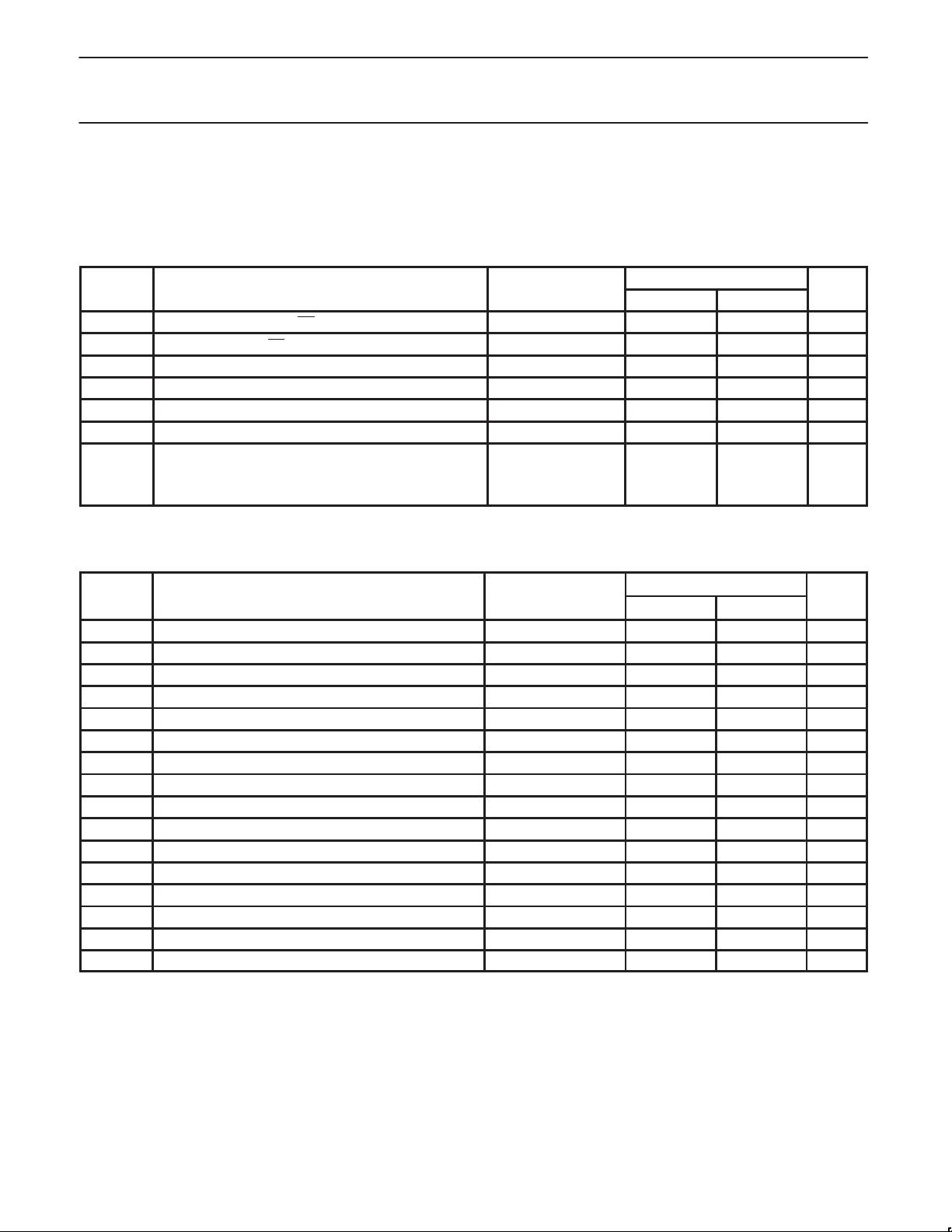
Electrical Deviations from Commercial Specifications for Extended Temperature Range
DC and AC parameters not included here are the same as in the commercial temperature range table.
DC ELECTRICAL CHARACTERISTICS
T
= –40°C to +85°C, VCC = 5V ±10% (87C550), VCC = 5V ±20% (80/83C550), VSS = 0V
amb
TEST LIMITS
SYMBOL PARAMETER CONDITIONS MIN MAX UNIT
V
IL
V
IL1
V
IH
V
IH1
I
IL
I
TL
I
CC
Input low voltage, except EA –0.5 0.2VCC–0.15 V
Input low voltage to EA 0 0.2VCC–0.35 V
Input high voltage, except XTAL1, RST 0.2VCC+1 VCC+0.5 V
Input high voltage to XTAL1, RST 0.7VCC+0.1 VCC+0.5 V
Logical 0 input current, ports 2, 3 VIN = 0.45V –75 µA
Logical 1-to-0 transition current, ports 2, 3 VIN = 2.0V –750 µA
Power supply current:
Active mode
Idle mode
Power down mode
VCC = 4.5–5.5V ,
Frequency range =
3.5 to 16MHz
35
6
50
mA
mA
µA
ADC DC ELECTRICAL CHARACTERISTICS
AVCC = 5V ±10%, AVSS = 0V, T
SYMBOL PARAMETER CONDITIONS MIN MAX UNIT
AV
CC
V
REF
AI
CC
AV
IN
AIC, C
t
ADS
t
ADC
Analog supply AVCC = VCC ± 0.2 4.5 5.5 V
Analog reference; AV
Analog operating supply current See note 1 3.0 mA
Analog input voltage AVSS – 0.2 AVCC + 0.2 V
Analog input capacitance 15 pF
IA
Sampling time 8t
Conversion time 40t
Ae Absolute voltage error ±1.5 LSB
E
RA
Relative accuracy ±1 LSB
OSe Offset error See note 1 ±1 LSB
Ge Gain error See note 1 0.4 %
M
CTC
Channel-to-channel matching ±1 LSB
Ct Crosstalk 0 – 100kHz –60 dB
Rref Resistance between AV
AI
ID
AI
PD
Idle mode supply current See note 4 50 µA
Power down supply current See note 4 50 µA
NOTES:
1. Conditions: V
inputs are connected to AVCC and AVSS, the current AICC will be increased by the register ladder current and may exceed the
V
REF–
maximum shown here.
= 4.99712V , V
REF+
2. The resistor ladder network is not disconnected in the power-down or idle modes. Thus to conserve power, the user must remove AV
V
.
REF+
3. If the A/D function is not required, or if the A/D function is only needed periodically, AV
the digital circuitry. Contents of ADCON and ADAT are not guaranteed to be valid. Digital inputs P1.0 to P1.7 will not function normally. No
digital outputs are present on these pins.
4. For this test, the Analog inputs must be at the supplies (either V
= –40°C to 85°C, unless otherwise specified
amb
+ AV
REF
REF–
and AV
REF+
= 0V. AICC value does not include the resistor ladder current. For the 40-pin package, where the
REF–
REF–
or VSS).
DD
TEST LIMITS
AVSS – 0.2 AVCC + 0.2 V
1.0 10.0 KΩ
can be removed without affecting the operation of
CC
CY
CY
CC
and
1998 May 01
15
Page 16
Philips Semiconductors Product specification
80C51 8-bit microcontroller family
80C550/83C550/87C550
4K/128 OTP/ROM/ROMless, 8 channel 8 bit A/D, watchdog timer
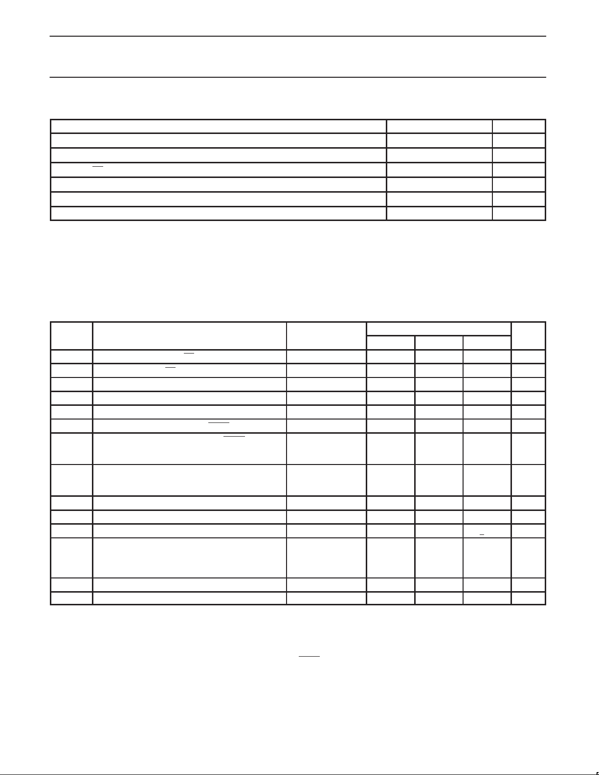
ABSOLUTE MAXIMUM RATINGS
Operating temperature under bias –40 to +85 °C
Storage temperature range –65 to +150 °C
Voltage on EA/VPP pin to VSS (87C550 only) 0 to +13.0 V
Voltage on any other pin to V
Input, output current on any two I/O pins ±10 mA
Power dissipation (based on package heat transfer limitations, not device power consumption) 1.5 W
NOTES:
1. Stresses above those listed under Absolute Maximum Ratings may cause permanent damage to the device. This is a stress rating only and
functional operation of the device at these or any conditions other than those described in the AC and DC Electrical Characteristics section
of this specification is not implied.
2. This product includes circuitry specifically designed for the protection of its internal devices from the damaging effects of excessive static
charge. Nonetheless, it is suggested that conventional precautions be taken to avoid applying greater than the rated maxima.
3. Parameters are valid over operating temperature range unless otherwise specified. All voltages are with respect to V
noted.
SS
1, 2, 3
PARAMETER RATING UNIT
–0.5 to +6.5 V
unless otherwise
SS
DC ELECTRICAL CHARACTERISTICS
T
= 0°C to +70°C or –40°C to +85°C, VCC = 5V ±10% (87C550), VCC = 5V ±20% (80/83C550), VSS = 0V
amb
TEST LIMITS
11.5
1.3
3
1
MAX UNIT
VCC+0.5 V
0.45 V
0.45 V
+10 µA
25
5
50
V
V
V
V
V
V
mA
mA
µA
SYMBOL PARAMETER CONDITIONS MIN TYPICAL
V
V
V
V
V
V
V
V
I
I
I
I
IL
TL
LI
CC
IL
IL1
IH
IH1
OL
OL1
OH
OH1
Input low voltage, except EA
Input low voltage to EA
Input high voltage, except XTAL1, RST
Input high voltage, XTAL1, RST
Output low voltage, ports 2, 3 IOL = 1.6mA
Output low voltage, port 0, ALE, PSEN IOL = 3.2mA
Output high voltage, ports 2, 3, ALE, PSEN
Output high voltage (port 0 in external bus mode) IOH = –800µA,
Logical 0 input current, ports 1, 2, 3
Logical 1-to-0 transition current, ports 1, 2, 3
Input leakage current, port 0 VIN = VIL or V
Power supply current (does not include AICC):7
Active mode @ 16MHz
7
7
7
7
2
2
3
IOH = –60µA,
I
= –25µA
OH
IOH = –10µA
–0.5 0.2VCC–0.1 V
0 0.2VCC–0.3 V
0.2VCC+0.9 VCC+0.5 V
0.7V
CC
2.4
0.75V
CC
0.9V
CC
2.4
IOH = –300µA
IOH = –80µA
7
7
5
VIN = 0.45V –50 µA
See note 4 –650 µA
See note 6
0.75V
CC
0.9V
CC
IH
Idle mode @ 16MHz
Power down mode
R
RST
C
IO
Internal reset pull-down resistor 50 300 kΩ
Pin capacitance (I/O pins only) 10 pF
NOTES:
1. Typical ratings are not guaranteed. The values listed are at room temperature, 5V.
2. Capacitive loading on ports 0 and 2 may cause spurious noise to be superimposed on the V
to external bus capacitance discharging into the port 0 and port 2 pins when these pins make 1-to-0 transitions during bus operations. In the
s of ALE and ports 1 and 3. The noise is due
OL
worst cases (capacitive loading > 100pF), the noise pulse on the ALE pin may exceed 0.8V . In such cases, it may be desirable to qualify
ALE with a Schmitt Trigger, or use an address latch with a Schmitt Trigger STROBE input.
3. Capacitive loading on ports 0 and 2 may cause the V
address bits are stabilizing.
on ALE and PSEN to momentarily fall below the 0.9VCC specification when the
OH
4. Pins of ports 2 and 3 source a transition current when they are being externally driven from 1 to 0. The transition current reaches its
maximum value when V
5. I
MAX at other frequencies is given by: Active mode; ICCMAX = 1.43 × FREQ + 1.90: Idle mode; ICCMAX = 0.14 × FREQ +2.31,
CC
where FREQ is the external oscillator frequency in MHz. I
6. See Figures 13 through 16 for I
7. These values apply only to T
is approximately 2V .
IN
test conditions.
CC
= 0°C to +70°C. For T
amb
MAX is given in mA. See Figure 12.
CC
= –40°C to +85°C. See table on previous page.
amb
1998 May 01
16
Page 17
Philips Semiconductors Product specification
80C51 8-bit microcontroller family
80C550/83C550/87C550
4K/128 OTP/ROM/ROMless, 8 channel 8 bit A/D, watchdog timer
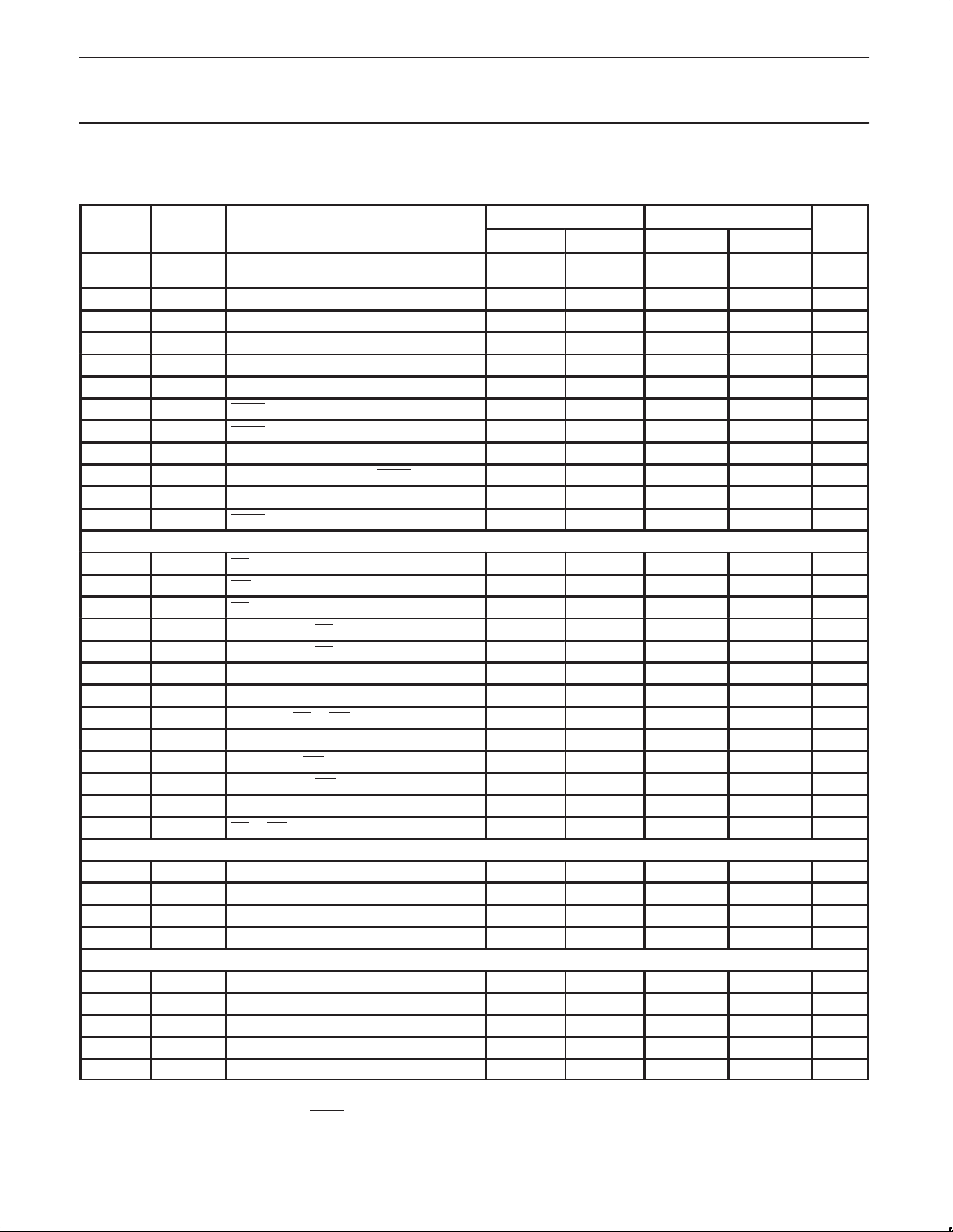
AC ELECTRICAL CHARACTERISTICS
T
= 0°C to +70°C or –40°C to +85°C, VCC = 5V ±10% (87C550), VCC = 5V ±20% (80/83C550), VSS = 0V
amb
16MHz CLOCK VARIABLE CLOCK
SYMBOL FIGURE PARAMETER MIN MAX MIN MAX UNIT
1/t
t
LHLL
t
AVLL
t
LLAX
t
LLIV
t
LLPL
t
PLPH
t
PLIV
t
PXIX
t
PXIZ
t
AVIV
t
PLAZ
CLCL
5 Oscillator frequency: Speed Versions
S8XC550 Exx
5 ALE pulse width 85 2t
5 Address valid to ALE low 7 t
5 Address hold after ALE low 27 t
5 ALE low to valid instruction in 150 4t
5 ALE low to PSEN low 22 t
5 PSEN pulse width 142 3t
5 PSEN low to valid instruction in 82 3t
5 Input instruction hold after PSEN 0 0 ns
5 Input instruction float after PSEN 37 t
5 Address to valid instruction in 207 5t
5 PSEN low to address float 10 10 ns
Data Memory
t
RLRH
t
WLWH
t
RLDV
t
RHDX
t
RHDZ
t
LLDV
t
AVDV
t
LLWL
t
AVWL
t
QVWX
t
WHQX
t
RLAZ
t
WHLH
6, 7 RD pulse width 275 6t
6, 7 WR pulse width 275 6t
6, 7 RD low to valid data in 212 5t
6, 7 Data hold after RD 0 0 ns
6, 7 Data float after RD 55 2t
6, 7 ALE low to valid data in 350 8t
6, 7 Address to valid data in 397 9t
6, 7 ALE low to RD or WR low 137 247 3t
6, 7 Address valid to WR low or RD low 120 4t
6, 7 Data valid to WR transition 12 t
6, 7 Data hold after WR 12 t
6, 7 RD low to address float 0 0 ns
6, 7 RD or WR high to ALE high 22 102 t
External Clock
t
CHCX
t
CLCX
t
CLCH
t
CHCL
9 High time 20 20 ns
9 Low time 20 20 ns
9 Rise time 20 20 ns
9 Fall time 20 20 ns
Shift Register
t
XLXL
t
QVXH
t
XHQX
t
XHDX
t
XHDV
8 Serial port clock cycle time 750 12t
8 Output data setup to clock rising edge 492 10t
8 Output data hold after clock rising edge 8 2t
8 Input data hold after clock rising edge 0 0 ns
8 Clock rising edge to input data valid 492 10t
NOTES:
1. Parameters are valid over operating temperature range unless otherwise specified.
2. Load capacitance for port 0, ALE, and PSEN
= 100pF, load capacitance for all other outputs = 80pF.
1, 2
3.5 16 MHz
–40 ns
CLCL
–55 ns
CLCL
–35 ns
CLCL
–100 ns
CLCL
–40 ns
CLCL
–45 ns
CLCL
–105 ns
CLCL
–25 ns
CLCL
–105 ns
CLCL
–100 ns
CLCL
–100 ns
CLCL
–165 ns
CLCL
–70 ns
CLCL
–150 ns
CLCL
–165 ns
CLCL
–50 3t
CLCL
–130 ns
CLCL
–50 ns
CLCL
–50 ns
CLCL
–40 t
CLCL
CLCL
–133 ns
CLCL
–117 ns
CLCL
+50 ns
CLCL
+40 ns
CLCL
–133 ns
CLCL
ns
1998 May 01
17
Page 18
Philips Semiconductors Product specification
80C51 8-bit microcontroller family
4K/128 OTP/ROM/ROMless, 8 channel 8 bit A/D, watchdog timer
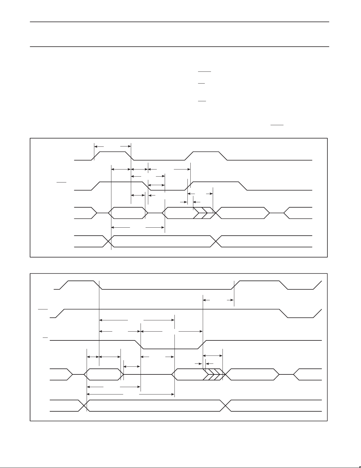
EXPLANATION OF THE AC SYMBOLS
Each timing symbol has five characters. The first character is always
‘t’ (= time). The other characters, depending on their positions,
indicate the name of a signal or the logical status of that signal. The
designations are:
A – Address
C – Clock
D – Input data
H – Logic level high
I – Instruction (program memory contents)
L – Logic level low, or ALE
t
ALE
PSEN
PORT 0
LHLL
t
t
AVLL
LLPL
t
LLAX
A0–A7 A0–A7
t
LLIV
t
PLIV
t
PLPH
t
PLAZ
t
P – PSEN
Q – Output data
R–RD
t – Time
V – Valid
W– WR
X – No longer a valid logic level
Z – Float
Examples: t
PXIX
INSTR IN
t
PXIZ
signal
signal
t
80C550/83C550/87C550
= Time for address valid to ALE low.
AVLL
= Time for ALE low to PSEN low.
LLPL
ALE
PSEN
PORT 0
PORT 2
RD
PORT 2
t
AVLL
t
LLAX
A0–A7
FROM RI OR DPL
t
AVWL
t
AVIV
A0–A15 A8–A15
Figure 5. External Program Memory Read Cycle
t
WHLH
t
LLDV
t
LLWL
t
RLAZ
t
AVDV
P2.0–P2.7 OR A8–A15 FROM DPF A0–A15 FROM PCH
t
RLDV
t
RLRH
t
RHDZ
t
RHDX
DATA IN A0–A7 FROM PCL INSTR IN
SU00006
1998 May 01
SU00025
Figure 6. External Data Memory Read Cycle
18
Page 19
Philips Semiconductors Product specification
80C51 8-bit microcontroller family
4K/128 OTP/ROM/ROMless, 8 channel 8 bit A/D, watchdog timer
ALE
PSEN
t
WLWH
DATA OUT A0–A7 FROM PCL INSTR IN
WR
PORT 0
PORT 2
t
AVLL
t
t
LLAX
A0–A7
FROM RI OR DPL
t
AVWL
LLWL
t
QVWX
P2.0–P2.7 OR A8–A15 FROM DPF A0–A15 FROM PCH
t
WHLH
80C550/83C550/87C550
t
WHQX
INSTRUCTION
ALE
CLOCK
OUTPUT DATA
WRITE TO SBUF
INPUT DATA
CLEAR RI
SU00069
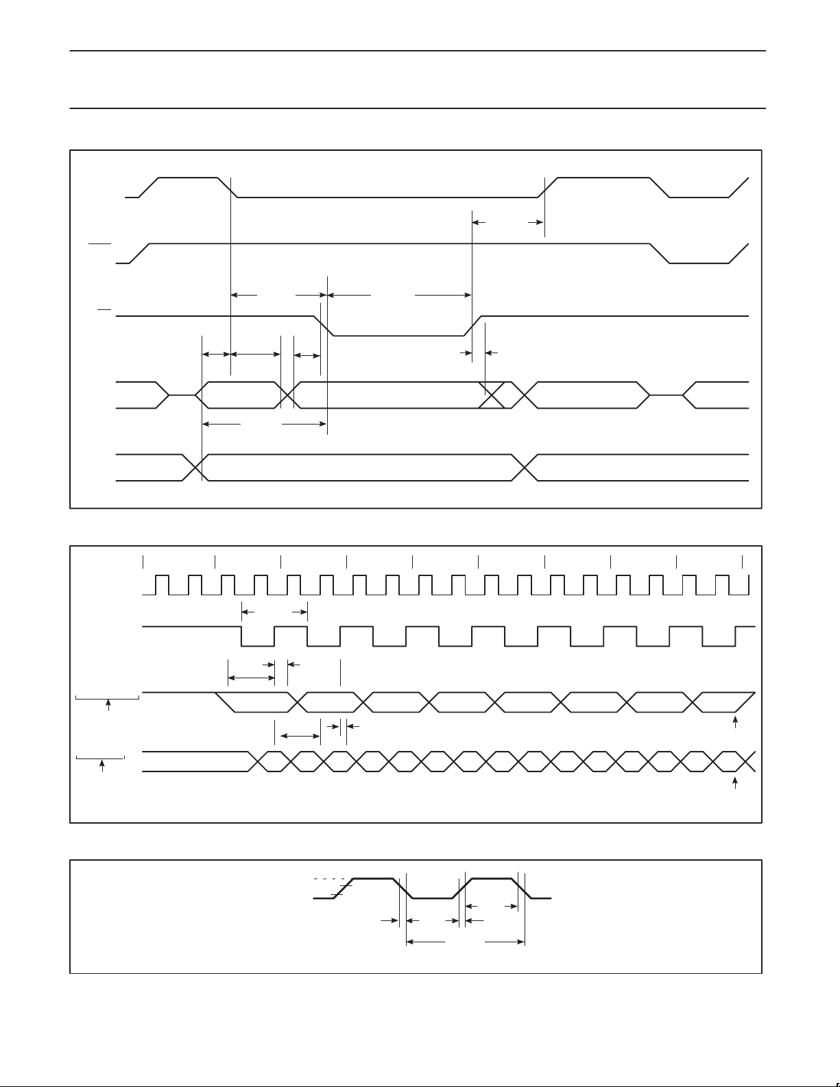
Figure 7. External Data Memory Write Cycle
012345678
t
XLXL
t
t
QVXH
t
XHDV
VALID VALID VALID VALID VALID VALID VALID VALID
XHQX
1230 4567
t
XHDX
SET TI
SET RI
SU00027
Figure 8. Shift Register Mode Timing
VCC–0.5
0.45V
0.7V
CC
0.2VCC–0.1
t
CHCL
t
CLCX
t
CLCL
t
CHCX
t
CLCH
SU00009
Figure 9. External Clock Drive
1998 May 01
19
Page 20
Philips Semiconductors Product specification
80C51 8-bit microcontroller family
4K/128 OTP/ROM/ROMless, 8 channel 8 bit A/D, watchdog timer
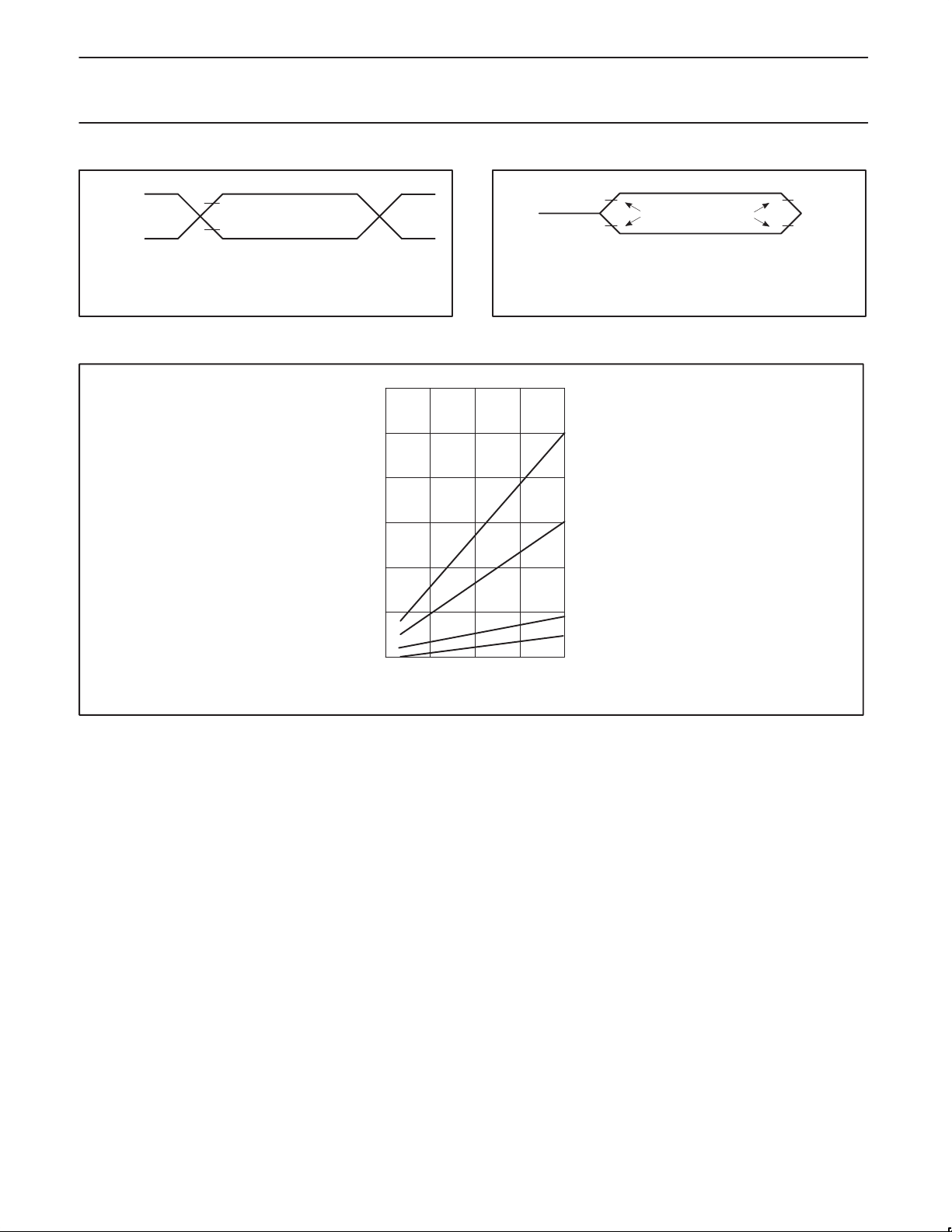
VCC–0.5
0.45V
NOTE:
AC inputs during testing are driven at VCC –0.5 for a logic ‘1’ and 0.45V for a logic ‘0’.
Timing measurements are made at VIH min for a logic ‘1’ and VIL max for a logic ‘0’.
Figure 10. AC Testing Input/Output
0.2V
0.2V
CC
CC
+0.9
–0.1
V
LOAD
NOTE:
For timing purposes, a port is no longer floating when a 100mV change from load
voltage occurs, and begins to float when a 100mV change from the loaded VOH/V
level occurs. IOH/IOL ≥ ±20mA.
SU00717
30
25
I
mA
CC
20
15
V
+0.1V
LOAD
V
–0.1V
LOAD
MAX ACTIVE MODE
TYP ACTIVE MODE
80C550/83C550/87C550
V
TIMING
REFERENCE
POINTS
Figure 11. Float Waveform
OH
V
OL
–0.1V
+0.1V
OL
SU00011
10
5
4MHz 8MHz 12MHz 16MHz
FREQ at XTAL1
MAX IDLE MODE
TYP IDLE MODE
SU00201
Figure 12. ICC vs. FREQ (Commercial Temp. Range)
Valid only within frequency specifications of the device under test
1998 May 01
20
Page 21
Philips Semiconductors Product specification
80C51 8-bit microcontroller family
4K/128 OTP/ROM/ROMless, 8 channel 8 bit A/D, watchdog timer
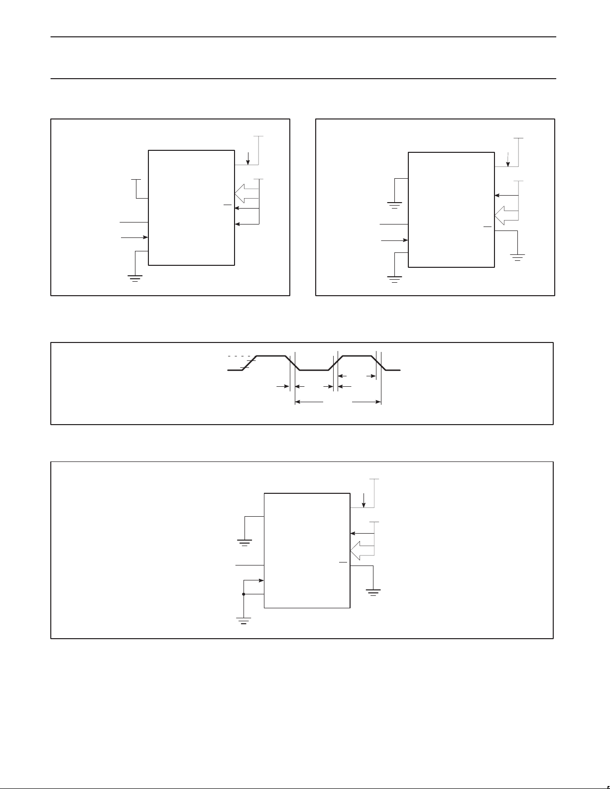
V
CC
I
CC
V
CC
P0
P1
V
CC
SU00202
CLOCK SIGNAL
V
CC
RST
(NC)
CLOCK SIGNAL
XTAL2
XTAL1
V
SS
Figure 13. ICC Test Condition, Active Mode
All other pins are disconnected
EA
80C550/83C550/87C550
V
RST
(NC)
XTAL2
XTAL1
V
SS
Figure 14. ICC Test Condition, Idle Mode
All other pins are disconnected
CC
P1
P0
EA
SU00203
V
CC
I
CC
V
CC
VCC–0.5
0.45V
0.7V
CC
0.2VCC–0.1
t
CHCL
t
CLCX
t
CLCL
t
CHCX
t
CLCH
SU00009
Figure 15. Clock Signal Waveform for ICC Tests in Active and Idle Modes
t
(NC)
CLCH
RST
XTAL2
XTAL1
V
SS
= t
CHCL
= 5ns
V
CC
I
CC
V
CC
P1
P0
EA
V
CC
SU00204
Figure 16. ICC Test Condition, Power Down Mode
All other pins are disconnected.
V
= 2V to 5.5V.
CC
1998 May 01
21
Page 22

Philips Semiconductors Product specification
80C51 8-bit microcontroller family
4K/128 OTP/ROM/ROMless, 8 channel 8 bit A/D, watchdog timer
EPROM CHARACTERISTICS
The 87C550 is programmed by using a modified Quick-Pulse
Programming algorithm. It differs from older methods in the value
used for V
number of the ALE/PROG
The 87C550 contains two signature bytes that can be read and used
by an EPROM programming system to identify the device. The
signature bytes identify the device as an S87C550 manufactured by
Philips.
Table 4 shows the logic levels for reading the signature byte, and for
programming the program memory, the encryption table, and the
lock bits. The circuit configuration and waveforms for quick-pulse
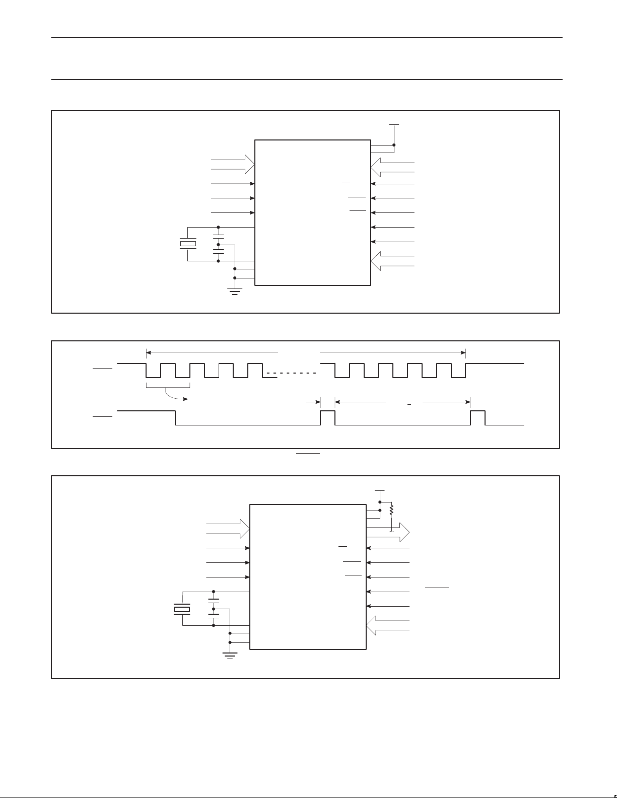
programming are shown in Figures 17 and 18. Figure 19 shows the
circuit configuration for normal program memory verification.
(programming supply voltage) and in the width and
PP
pulses.
Quick-Pulse Programming
The setup for microcontroller quick-pulse programming is shown in
Figure 17. Note that the 87C550 is running with a 4 to 6MHz
oscillator. The reason the oscillator needs to be running is that the
device is executing internal address and program data transfers.
The address of the EPROM location to be programmed is applied to
ports 2 and 3, as shown in Figure 17. The code byte to be
programmed into that location is applied to port 0. RST, PSEN
pins of ports 1 and 2 specified in Table 4 are held at the ‘Program
Code Data’ levels indicated in Table 4. The ALE/PROG
low 25 times as shown in Figure 18.
To program the encryption table, repeat the 25 pulse programming
sequence for addresses 0 through 1FH, using the ‘Pgm Encryption
Table’ levels. Do not forget that after the encryption table is
programmed, verification cycles will produce only encrypted data.
To program the security bits, repeat the 25 pulse programming
sequence using the ‘Pgm Security Bit’ levels. After one security bit is
and
is pulsed
programmed, further programming of the code memory and
encryption table is disabled. However, the other security bit can still
be programmed.
Note that the EA
maximum specified V
glitch above that voltage can cause permanent damage to the
device. The V
and overshoot.
Program Verification
If security bit 2 has not been programmed, the on-chip program
memory can be read out for program verification. The address of the
program memory locations to be read is applied to ports 2 and 3 as
shown in Figure 19. The other pins are held at the ‘Verify Code Data’
levels indicated in Table 4. The contents of the address location will
be emitted on port 0. External pull-ups are required on port 0 for this
operation.
If the encryption table has been programmed, the data presented at
port 0 will be the exclusive NOR of the program byte with one of the
encryption bytes. The user will have to know the encryption table
contents in order to correctly decode the verification data. The
encryption table itself cannot be read out.
Reading the Signature Bytes
The signature bytes are read by the same procedure as a normal
verification of locations 030H and 031H, except that P1.0 and P1.1
need to be pulled to a logic low. The values are:
(030H) = 15H indicates manufactured by Philips
(031H) = 96H indicates S87C550
Program/Verify Algorithms
Any algorithm in agreement with the conditions listed in Table 4, and
which satisfies the timing specifications, is suitable.
80C550/83C550/87C550
/VPP pin must not be allowed to go above the
level for any amount of time. Even a narrow
PP
source should be well regulated and free of glitches
PP
Table 4. EPROM Programming Modes
MODE RST PSEN ALE/PROG EA/V
Read signature 1 0 1 1 0 0 0 0
Program code data 1 0 0* V
Verify code data 1 0 1 1 0 0 1 1
Pgm encryption table 1 0 0* V
Pgm security bit 1 1 0 0* V
Pgm security bit 2 1 0 0* V
NOTES:
1. ’0’ = Valid low for that pin, ’1’ = valid high for that pin.
= 12.75V ±0.25V.
2. V
PP
= 5V±10% during programming and verification.
3. V
CC
* ALE/PROG
minimum of 10µs.
Trademark phrase of Intel Corporation.
receives 25 programming pulses while VPP is held at 12.75V . Each programming pulse is low for 100 µs (±10µs) and high for a
PP
PP
PP
PP
PP
P2.7 P2.6 P1.1 P1.0
1 0 1 1
1 0 1 0
1 1 1 1
1 1 0 0
1998 May 01
22
Page 23
Philips Semiconductors Product specification
80C51 8-bit microcontroller family
4K/128 OTP/ROM/ROMless, 8 channel 8 bit A/D, watchdog timer
A0–A7
1
1
1
4–6MHz
P3
RST
P1.0
P1.1
XTAL2
XTAL1
AV
SS
V
SS
87C550
EA
ALE/PROG
P2.0–P2.4
Figure 17. Programming Configuration
AV
V
/V
PSEN
P2.7
P2.6
CC
CC
PP
80C550/83C550/87C550
+5V
P0
PGM DATA
+12.75V
25 100µs PULSES TO GROUND
0
1
0
A8–A11
SU00205
ALE/PROG:
ALE/PROG:
1
0
4–6MHz
25 PULSES
1
0
100µs+1010µs MIN
SU00018
Figure 18. PROG Waveform
+5V
AV
CC
V
A0–A7
P3
1
1
1
RST
P1.0
P1.1
XTAL2
XTAL1
AV
SS
V
SS
87C550
CC
/V
EA
PP
ALE/PROG
PSEN
P2.7
P2.6
P2.0–P2.4
P0
PGM Data
1
1
0
0 ENABLE
0
A8–A11
1998 May 01
SU00206
Figure 19. Program Verification
23
Page 24
Philips Semiconductors Product specification
80C51 8-bit microcontroller family
4K/128 OTP/ROM/ROMless, 8 channel 8 bit A/D, watchdog timer
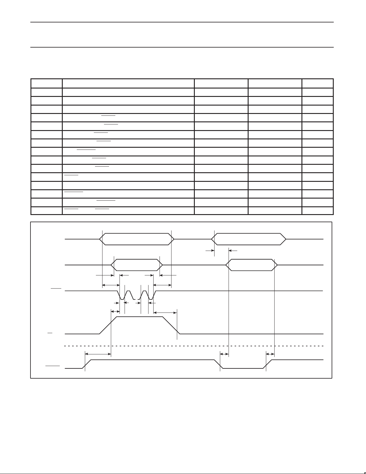
EPROM PROGRAMMING AND VERIFICATION CHARACTERISTICS
T
= 21°C to +27°C, VCC = 5V±10%, VSS = 0V (See Figure 20)
amb
SYMBOL
V
PP
I
PP
1/t
CLCL
t
AVGL
t
GHAX
t
DVGL
t
GHDX
t
EHSH
t
SHGL
t
GHSL
t
GLGH
t
AVQV
t
ELQZ
t
EHQZ
t
GHGL
Programming supply voltage 12.5 13.0 V
Programming supply current 50 mA
Oscillator frequency 4 6 MHz
Address setup to PROG low 48t
Address hold after PROG 48t
Data setup to PROG low 48t
Data hold after PROG 48t
P2.7 (ENABLE) high to V
VPP setup to PROG low 10 µs
VPP hold after PROG 10 µs
PROG width 90 110 µs
Address to data valid 48t
ENABLE low to data valid 48t
Data float after ENABLE 0 48t
PROG high to PROG low 10 µs
PARAMETER MIN MAX UNIT
PP
48t
80C550/83C550/87C550
CLCL
CLCL
CLCL
CLCL
CLCL
CLCL
CLCL
CLCL
P3.0–P3.7
P2.0–P2.4
PORT 0
t
ALE/PROG
EA/V
PP
P2.7
ENABLE
DVGL
t
EHSH
t
GLGH
t
SHGL
t
AVGL
NOTE:
FOR PROGRAMMING VERIFICATION, SEE FIGURE 17.
*
FOR VERIFICATION CONDITIONS, SEE FIGURE 19.
PROGRAMMING* VERIFICATION*
ADDRESS ADDRESS
t
AVQV
DATA IN DATA OUT
t
t
GHAX
t
GHGL
t
LOGIC 0
GHSL
GHDX
LOGIC 1 LOGIC 1
t
ELQV
Figure 20. EPROM Programming and Verification
t
EHQZ
SU00207
1998 May 01
24
Page 25
Philips Semiconductors Product specification
80C51 8-bit microcontroller family
80C550/83C550/87C550
4K/128 OTP/ROM/ROMless, 8 channel 8 bit A/D, watchdog timer
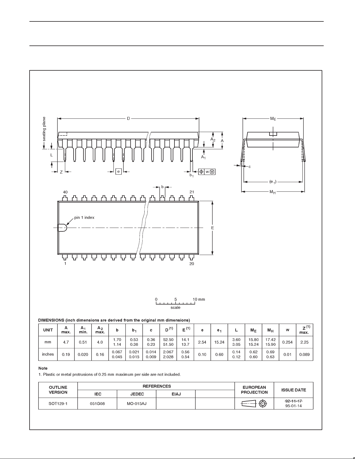
DIP40: plastic dual in-line package; 40 leads (600 mil) SOT129-1
1998 May 01
25
Page 26
Philips Semiconductors Product specification
80C51 8-bit microcontroller family
80C550/83C550/87C550
4K/128 OTP/ROM/ROMless, 8 channel 8 bit A/D, watchdog timer
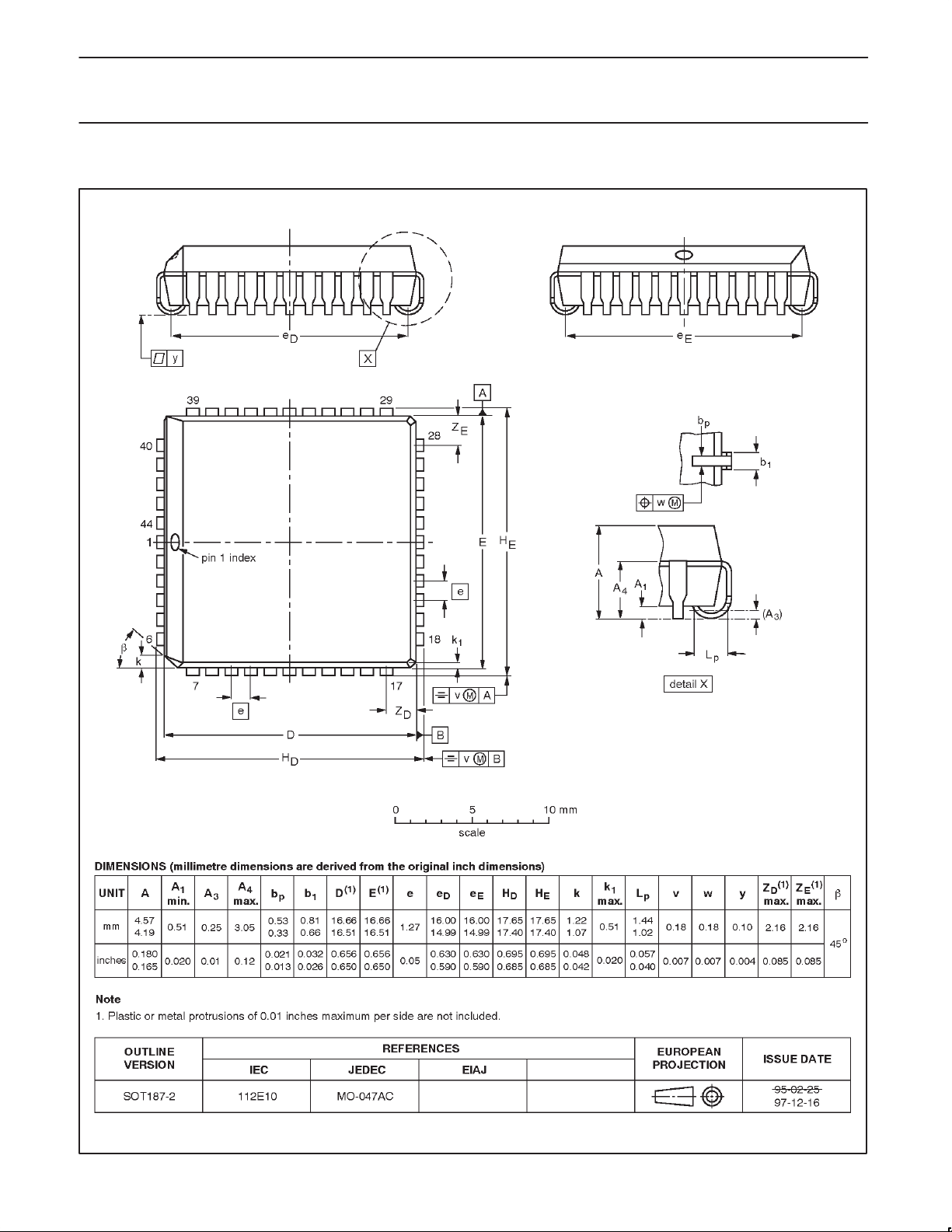
PLCC44: plastic leaded chip carrier; 44 leads SOT187-2
1998 May 01
26
Page 27

Philips Semiconductors Product specification
80C51 8-bit microcontroller family
4K/128 OTP/ROM/ROMless, 8 channel 8 bit A/D, watchdog timer
NOTES
80C550/83C550/87C550
1998 May 01
27
Page 28

Philips Semiconductors Product specification
80C51 8-bit microcontroller family
4K/128 OTP/ROM/ROMless, 8 channel 8 bit A/D, watchdog timer
Data sheet status
Data sheet
status
Objective
specification
Preliminary
specification
Product
specification
Product
status
Development
Qualification
Production
Definition
This data sheet contains the design target or goal specifications for product development.
Specification may change in any manner without notice.
This data sheet contains preliminary data, and supplementary data will be published at a later date.
Philips Semiconductors reserves the right to make chages at any time without notice in order to
improve design and supply the best possible product.
This data sheet contains final specifications. Philips Semiconductors reserves the right to make
changes at any time without notice in order to improve design and supply the best possible product.
[1]
80C550/83C550/87C550
[1] Please consult the most recently issued datasheet before initiating or completing a design.
Definitions
Short-form specification — The data in a short-form specification is extracted from a full data sheet with the same type number and title. For
detailed information see the relevant data sheet or data handbook.
Limiting values definition — Limiting values given are in accordance with the Absolute Maximum Rating System (IEC 134). Stress above one
or more of the limiting values may cause permanent damage to the device. These are stress ratings only and operation of the device at these or
at any other conditions above those given in the Characteristics sections of the specification is not implied. Exposure to limiting values for extended
periods may affect device reliability.
Application information — Applications that are described herein for any of these products are for illustrative purposes only. Philips
Semiconductors make no representation or warranty that such applications will be suitable for the specified use without further testing or
modification.
Disclaimers
Life support — These products are not designed for use in life support appliances, devices or systems where malfunction of these products can
reasonably be expected to result in personal injury . Philips Semiconductors customers using or selling these products for use in such applications
do so at their own risk and agree to fully indemnify Philips Semiconductors for any damages resulting from such application.
Right to make changes — Philips Semiconductors reserves the right to make changes, without notice, in the products, including circuits, standard
cells, and/or software, described or contained herein in order to improve design and/or performance. Philips Semiconductors assumes no
responsibility or liability for the use of any of these products, conveys no license or title under any patent, copyright, or mask work right to these
products, and makes no representations or warranties that these products are free from patent, copyright, or mask work right infringement, unless
otherwise specified.
Philips Semiconductors
811 East Arques Avenue
P.O. Box 3409
Sunnyvale, California 94088–3409
Telephone 800-234-7381
Copyright Philips Electronics North America Corporation 1998
All rights reserved. Printed in U.S.A.
Date of release: 05-98
Document order number: 9397 750 03853
1998 May 01
28
 Loading...