

Page 1

INTEGRATED CIRCUITS
87C524/87C528
80C51 8-bit microcontrollers
16K/32K, 512 OTP, I2C, watchdog timer
Product specification
Replaces data sheets 87C524 of 1998 May 01 and 87C528 of 1998 May 01
IC28 Data Handbook
1999 Jul 23
Page 2
Philips Semiconductors Product specification
80C51 8-bit microcontrollers
2
16K/32K, 512 OTP, I
DESCRIPTION
The 87C528 single-chip 8-bit microcontroller is manufactured in an
advanced CMOS process and is a derivative of the 80C51
microcontroller family. The 87C528 has the same instruction set as
the 80C51. Three versions of the derivative exist:
•83C528—32k bytes ROM
•83C524—16k bytes ROM
•80C528—ROMless version of the 83C528
•87C528—32k bytes EPROM
•87C524—16k bytes EPROM
This device provides architectural enhancements that make it
applicable in a variety of applications in consumer, telecom and
general control systems, especially in those systems which need
large ROM and RAM capacity on-chip.
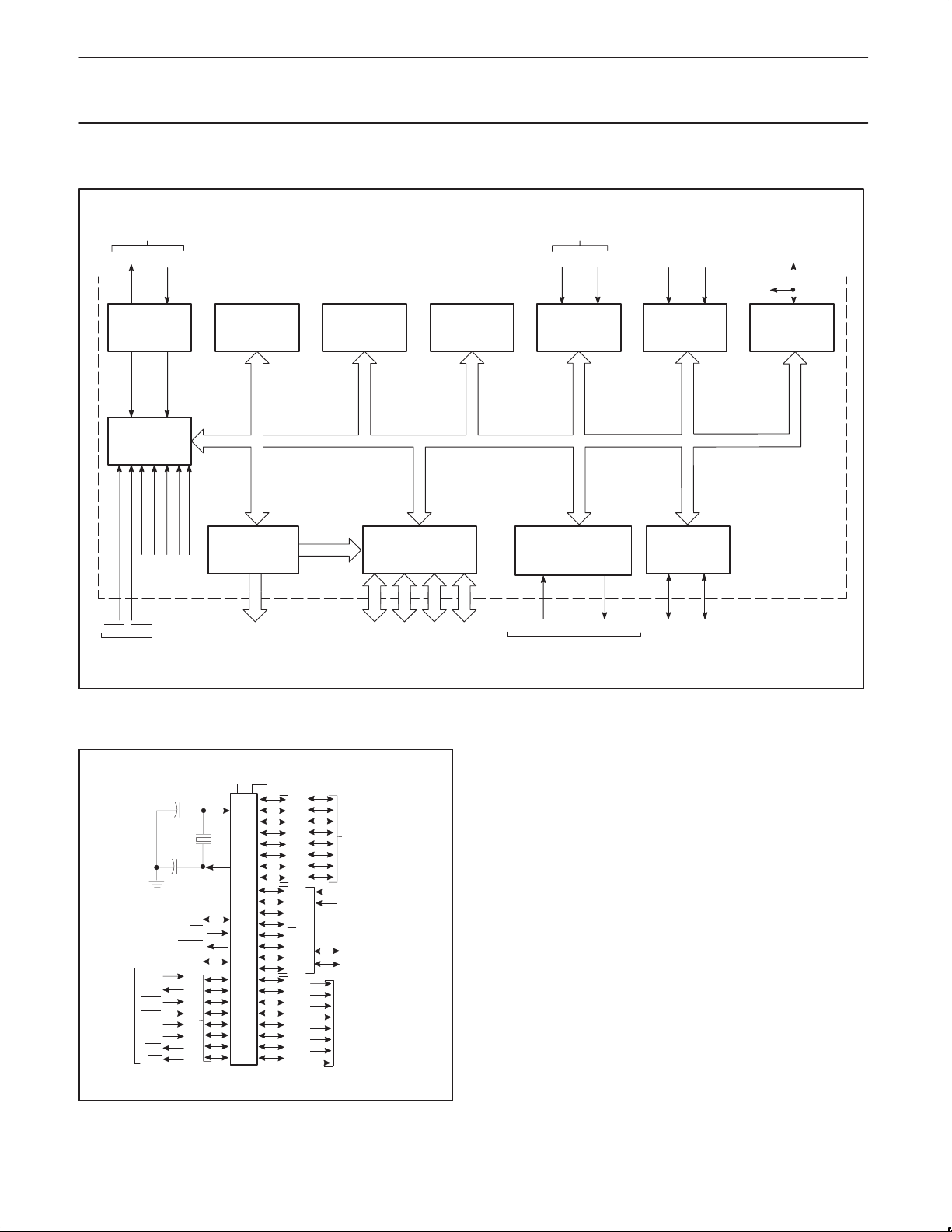
The 87C528 contains a 32k × 8 EPROM and the 87C524 contains a
16k x 8 EPROM. Both devices have a 512 × 8 RAM, four 8-bit I/O
ports, two 16-bit timer/event counters (identical to the timers of the
80C51), a 16-bit timer (identical to the timer 2 of the 80C52), a
watchdog timer with a separate oscillator, a multi-source,
two-priority-level, nested interrupt structure, two serial interfaces
(UART and I
In addition, the 87C524/87C528 has two software selectable modes
of power reduction—idle mode and power-down mode. The idle
mode freezes the CPU while allowing the RAM, timers, serial port,
and interrupt system to continue functioning. The power-down mode
saves the RAM contents but freezes the oscillator, causing all other
chip functions to be inoperative.
2
C-bus), and on-chip oscillator and timing circuits.
C, watchdog timer
FEA TURES
•80C51 instruction set
– 512 × 8 RAM
– Memory addressing capability
64k ROM and 64k RAM
– Three 16-bit counter/timers
– On-chip watchdog timer with oscillator
– Full duplex UART
2
C serial interface
– I
•Power control modes:
– Idle mode
– Power-down mode
– Warm start from power-down
•CMOS and TTL compatible
•Extended temperature ranges
•EPROM code protection
•OTP package available
•16 MHz speed at V
CC
= 5 V
87C524/87C528
ORDERING INFORMATION
EPROM
P87C528EBP N 0 to +70, Plastic Dual In-line Package 16 SOT129-1
P87C528EBA A 0 to +70, Plastic Leaded Chip Carrier 16 SOT187-2
P87C528EBB B 0 to +70, Plastic Quad Flat Pack 16 SOT307-2
P87C528EFP N –40 to +85, Plastic Dual In-line Package 16 SOT129-1
P87C528EFB B –40 to +85, Plastic Quad Flat Pack 16 SOT307-2
P87C524EBA A 0 to +70, Plastic Leaded Chip Carrier 16 SOT187-2
P87C524EBB B 0 to +70, Plastic Quad Flat Pack 16 SOT307-2
NOTE:
1. For ROM & ROMless devices, see data sheet P8X524/528.
1999 Jul 23 853-1687 22041
TEMPERATURE oC RANGE
AND PACKAGE
2
FREQ
(MHz)
Drawing
Number
Page 3
Philips Semiconductors Product specification
80C51 8-bit microcontrollers
2
16K/32K, 512 OTP, I
BLOCK DIAGRAM
FREQUENCY
REFERENCE
XTAL2 XTAL1
OSCILLATOR
AND
TIMING
CPU
PROGRAM
MEMORY
(32K x 8
EPROM)
C, watchdog timer
RAM AUX–RAM
DATA
MEMORY
(256 x 8)
DATA
MEMORY
(256 x 8)
COUNTERS
T0 T1
TWO 16-BIT
TIMER/EVENT
COUNTERS
87C524/87C528
T2 T2EX
16-BIT TIMER/
EVENT COUNTER
RST
WATCHDOG
TIMER
INTERNAL
INTERRUPTS
INT0
INT1
EXTERNAL
INTERRUPTS
LOGIC SYMBOL
RST
PSEN
ALE
RxD
TxD
INT0
INT1
T0
T1
WR
RD
SECONDARY FUNCTIONS
XTAL1
XTAL2
EA
PORT 3
64K-BYTE BUS
EXPANSION
CONTROL
CONTROL
V
V
SS
DD
PORT 0
PORT 1PORT 2
PROGRAMMABLE I/O
PARALLEL PORTS,
ADDRESS/DATA BUS
AND I/O PINS
ADDRESS AND
DATA BUS
T2
T2EX
SCL
SDA
ADDRESS BUS
SU00165
PROGRAMMABLE
SERIAL PORT
FULL DUPLEX UART
SYNCHRONOUS SHIFT
SERIAL IN SERIAL OUT
SHARED WITH
PORT 3
BIT-LEVEL
2
I
C
INTERFACE
SDA SCL
SU00166
1999 Jul 23
3
Page 4
Philips Semiconductors Product specification
80C51 8-bit microcontrollers
2
16K/32K, 512 OTP, I
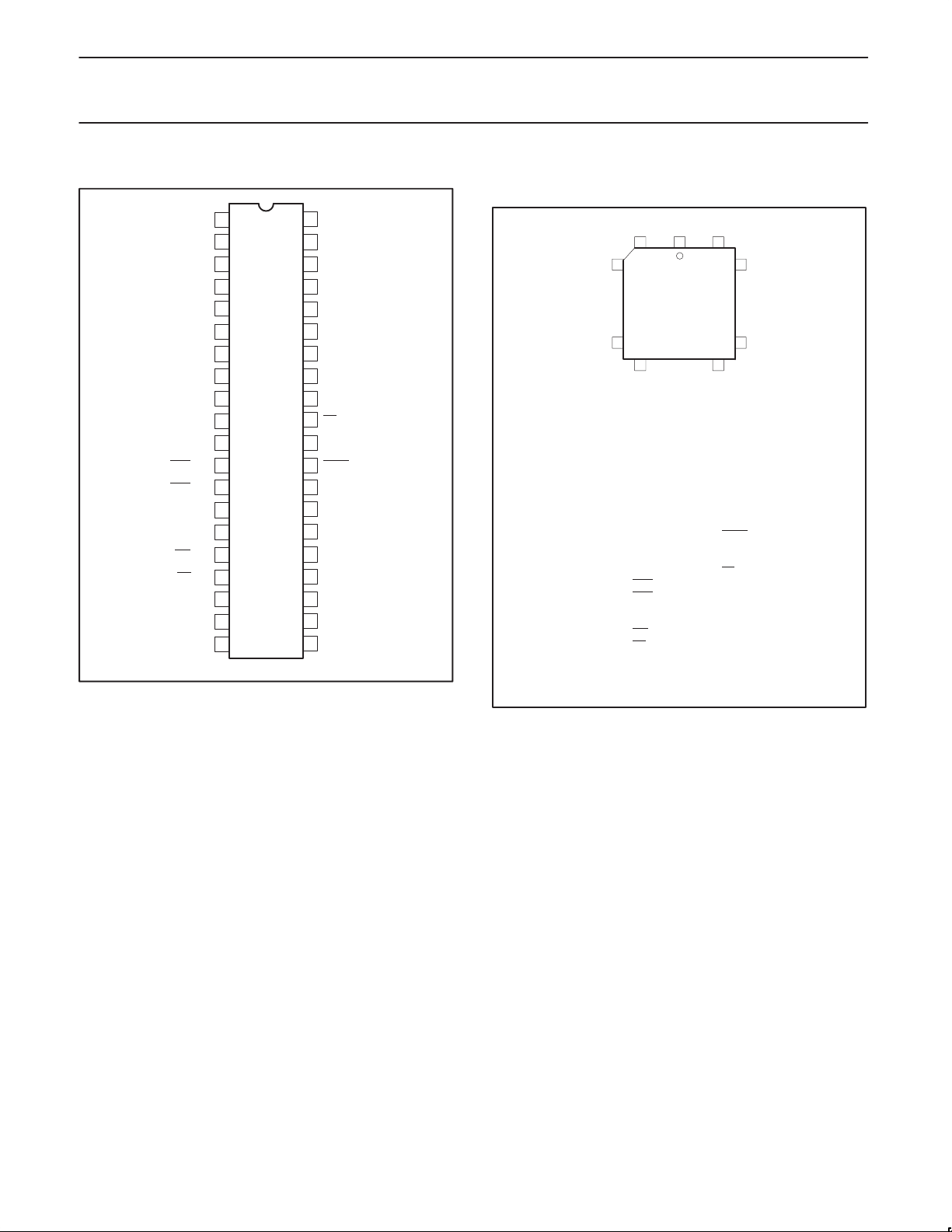
PIN CONFIGURATIONS
1
T2/P1.0
T2EX/P1.1
SCL/P1.6
SDA/P1.7
RxD/P3.0
TxD/P3.1
INT0
INT1
WR
P1.2
P1.3
P1.4
P1.5
RST
/P3.2
/P3.3
T0/P3.4
T1/P3.5
/P3.6
RD
/P3.7
XTAL2
XTAL1
V
2
3
4
5
6
7
8
9
10
PACKAGE
11
12
13
14
15
16
17
18
19
20
SS
DUAL
IN-LINE
C, watchdog timer
40
V
39
P0.0/AD0
38
P0.1/AD1
37
P0.2/AD2
36
P0.3/AD3
35
P0.4/AD4
34
P0.5/AD5
33
P0.6/AD6
32
P0.7/AD7
31
EA
30
ALE
29
PSEN
28
P2.7/A15
27
P2.6/A14
26
P2.5/A13
25
P2.4/A12
24
P2.3/A11
23
P2.2/A10
22
P2.1/A9
21
P2.0/A8
DD
SU00162
87C524/87C528
PLASTIC LEADED CHIP CARRIER PIN FUNCTIONS
6140
7
LCC
17
18 28
Pin Function
1 NC*
2 P1.0/T2
3 P1.1/T2EX
4 P1.2
5 P1.3
6 P1.4
7 P1.5
8 P1.6/SCL
9 P1.7/SDA
10 RST
11 P3.0/RxD
12 NC*
13 P3.1/TxD
14 P3.2/INT0
15 P3.3/INT1
16 P3.4/T0
17 P3.5/T1
18 P3.6/WR
19 P3.7/RD
20 XTAL2
21 XTAL1
22 V
SS
* NO INTERNAL CONNECTIONS
Pin Function
23 NC*
24 P2.0/A8
25 P2.1/A9
26 P2.2/A10
27 P2.3/A11
28 P2.4/A12
29 P2.5/A13
30 P2.6/A14
31 P2.7/A15
32 PSEN
33 ALE
34 NC*
35 EA
36 P0.7/AD7
37 P0.6/AD6
38 P0.5/AD5
39 P0.4/AD4
40 P0.3/AD3
41 P0.2/AD2
42 P0.1/AD1
43 P0.0/AD0
44 V
DD
39
29
SU00163A
1999 Jul 23
4
Page 5
Philips Semiconductors Product specification
80C51 8-bit microcontrollers
2
16K/32K, 512 OTP, I
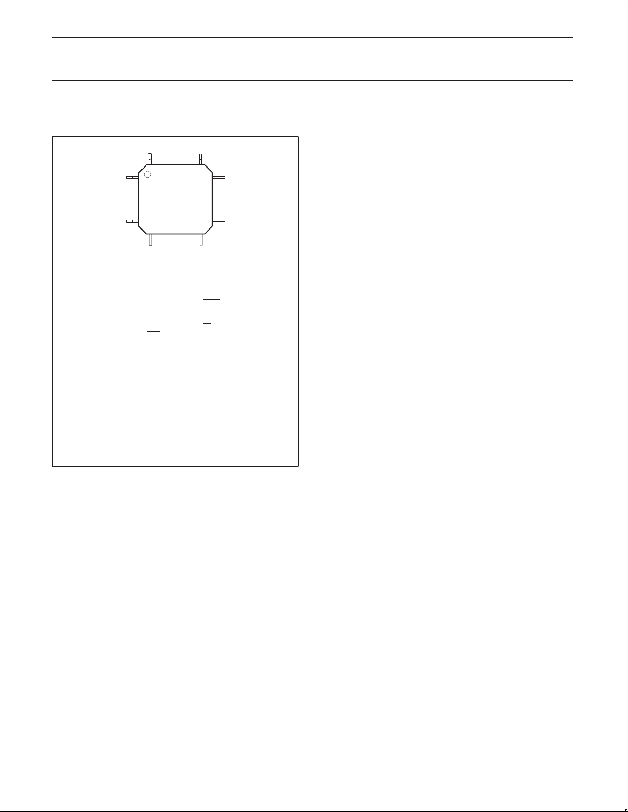
PLASTIC QUAD FLAT PACK PIN FUNCTIONS
44 34
1
QFP
11
12 22
Pin Function
1 P1.5
2 P1.6/SCL
3 P1.7/SDA
4 RST
5 P3.0/RxD
6 NC*
7 P3.1/TxD
8 P3.2/INT0
9 P3.3/INT1
10 P3.4/T0
11 P3.5/T1
12 P3.6/WR
13 P3.7/RD
14 XTAL2
15 XTAL1
16 V
SS
17 NC*
18 P2.0/A8
19 P2.1/A9
20 P2.2/A10
21 P2.3/A11
22 P2.4/A12
* NO INTERNAL CONNECTIONS
C, watchdog timer
Pin Function
23 P2.5/A13
24 P2.6/A14
25 P2.7/A15
26 PSEN
27 ALE
28 NC*
29 EA
30 P0.7/AD7
31 P0.6/AD6
32 P0.5/AD5
33 P0.4/AD4
34 P0.3/AD3
35 P0.2/AD2
36 P0.1/AD1
37 P0.0/AD0
38 V
DD
39 NC*
40 P1.0/T2
41 P1.1/T2EX
42 P1.2
43 P1.3
44 P1.4
SU00164
87C524/87C528
33
23
1999 Jul 23
5
Page 6

Philips Semiconductors Product specification
80C51 8-bit microcontrollers
2
16K/32K, 512 OTP, I
C, watchdog timer
87C524/87C528
PIN DESCRIPTIONS
PIN NO.
MNEMONIC DIP LCC QFP TYPE NAME AND FUNCTION
V
SS
V
DD
P0.0–0.7 39–32 43–36 37–30 I/O Port 0: Port 0 is an open-drain, bidirectional I/O port. Port 0 pins that have 1s written to
P1.0–P1.7 1–8 2–9 40–44
P2.0–P2.7 21–28 24–31 18–25 I/O Port 2: Port 2 is an 8-bit bidirectional I/O port with internal pull-ups. Port 2 pins that have
P3.0–P3.7 10–17 11,
RST 9 10 4 I/O Reset: A high on this pin for two machine cycles while the oscillator is running, resets the
ALE 30 33 27 I/O Address Latch Enable: Output pulse for latching the low byte of the address during an
PSEN 29 32 26 O Program Store Enable: The read strobe to external program memory. When the device is
EA 31 35 29 I External Access Enable: EA must be externally held low during RESET to enable the
XTAL1 19 21 15 I Crystal 1: Input to the inverting oscillator amplifier and input to the internal clock generator
XTAL2 18 20 14 O Crystal 2: Output from the inverting oscillator amplifier.
20 22 16 I Ground: circuit ground potential.
40 44 38 I Power Supply: +5 V power supply pin during normal operation, Idle mode and
1–3
1 2 40 I T2 (P1.0): Timer/counter 2 external count input (following edge triggered).
2 3 41 I T2EX (P1.1): T imer/counter 2 trigger input.
7 8 2 I/O SCL (P1.6): I2C serial port clock line.
8 9 3 I/O SDA (P1.7): I2C serial port data line.
13–19
10 11 5 I RxD (P3.0): Serial input port
11 13 7 O TxD (P3.1): Serial output port
12 14 8 I INT0 (P3.2): External interrupt
13 15 9 I INT1 (P3.3): External interrupt
14 16 10 I T0 (P3.4): Timer 0 external input
15 17 11 I T1 (P3.5): T imer 1 external input
16 18 12 O WR (P3.6): External data memory write strobe
17 19 13 O RD (P3.7): External data memory read strobe
5,
7–13
Power-down mode.
them float and can be used as high-impedance inputs. Port 0 is also the multiplexed
low-order address and data bus during accesses to external program and data memory. In
this application, it uses strong internal pull-ups when emitting 1s.
I/O Port 1: Port 1 is an 8-bit bidirectional I/O port with internal pull-ups, except P1.6 and P1.7
which have open drain. Port 1 pins that have 1s written to them are pulled high by the
internal pull-ups and can be used as inputs. As inputs, port 1 pins that are externally pulled
low will source current because of the internal pull-ups. (See DC Electrical Characteristics:
I
). Port 1 can sink/source one TTL (4 LSTTL) inputs. Port 1 receives the low-order
IL
address byte during program memory verification. Port 1 also serves alternate functions for
timer 2:
1s written to them are pulled high by the internal pull-ups and can be used as inputs. As
inputs, port 2 pins that are externally being pulled low will source current because of the
internal pull-ups. (See DC Electrical Characteristics: I
address byte during fetches from external program memory and during accesses to
external data memory that use 16-bit addresses (MOVX @DPTR). In this application, it
uses strong internal pull-ups when emitting 1s. During accesses to external data memory
that use 8-bit addresses (MOV @Ri), port 2 emits the contents of the P2 special function
register.
I/O Port 3: Port 3 is an 8-bit bidirectional I/O port with internal pull-ups. Port 3 pins that have
1s written to them are pulled high by the internal pull-ups and can be used as inputs. As
inputs, port 3 pins that are externally being pulled low will source current because of the
pull-ups. (See DC Electrical Characteristics: I
the SC80C51 family , as listed below:
device. An internal diffused resistor to V
capacitor to V
reset signal is active.
access to external memory. In normal operation, ALE is emitted at a constant rate of 1/6
the oscillator frequency , and can be used for external timing or clocking. Note that one ALE
pulse is skipped during each access to external data memory.
executing code from the external program memory, PSEN
cycle, except that two PSEN
memory. PSEN
device to fetch code from external program memory locations 0000H to 7FFFH. If EA
held high during RESET, the device executes from internal program memory unless the
program counter contains an address greater than 7FFFH. EA
circuits.
. After a watchdog timer overflow, this pin is pulled high while the internal
DD
is not activated during fetches from internal program memory.
activations are skipped during each access to external data
IL
permits a power-on reset using only an external
SS
). Port 2 emits the high-order
IL
). Port 3 also serves the special features of
is activated twice each machine
is don’t care after RESET.
is
1999 Jul 23
6
Page 7
Philips Semiconductors Product specification
80C51 8-bit microcontrollers
2
16K/32K, 512 OTP, I
C, watchdog timer
87C524/87C528
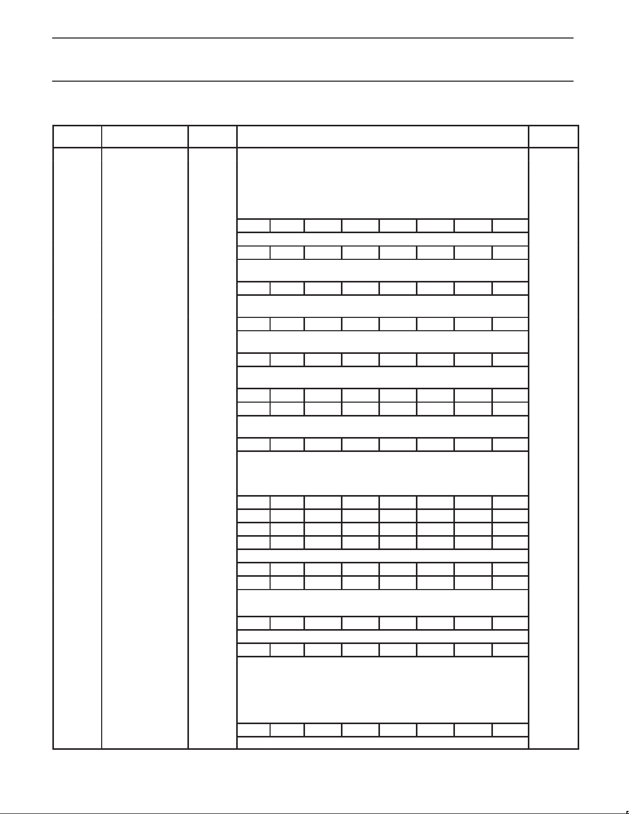
Table 1. 8XC524/8XC528 Special Function Registers
SYMBOL DESCRIPTION
ACC* Accumulator E0H E7 E6 E5 E4 E3 E2 E1 E0 00H
B* B register F0H F7 F6 F5 F4 F3 F2 F1 F0 00H
DPTR:
DPH
DPL
IE*# Interrupt enable A8H EA ES1 ET2 ES0 ET1 EX1 ET0 EX0 00H
IP*# Interrupt priority B8H – PS1 PT2 PS0 PT1 PX1 PT0 PX0 x0000000B
P0* Port 0 80H AD7 AD6 AD5 AD4 AD3 AD2 AD1 AD0 FFH
P1* Port 1 90H SDA SEL – – – – T2EX T2 FFH
P2* Port 2 A0H A15 A14 A13 A12 A11 A10 A9 A8 FFH
Data pointer (2 bytes):
Data pointer high
Data pointer low
DIRECT
ADDRESS
83H
82H
BIT ADDRESS, SYMBOL, OR ALTERNATIVE PORT FUNCTION
MSB LSB
AF AE AD AC AB AA A9 A8
BF BE BD BC BB BA B9 B8
87 86 85 84 83 82 81 80
97 96 95 94 93 92 91 90
A7 A6 A5 A4 A3 A2 A1 A0
RESET
VALUE
00H
00H
B7 B6 B5 B4 B3 B2 B1 B0
P3* Port 3 B0H RD WR T1 T0 INT1 INT0 TxD RxD FFH
PCON Power control 87H SMOD – – – GF1 GF0 PD IDL 0xxx0000B
D7 D6 D5 D4 D3 D2 D1 D0
PSW* Program status word D0H CY AC F0 RS1 RS0 OV F1 P 00H
RCAP2H#
RCAP2L#
SBUF
SCON* Serial controller 98H SM0 SM1 SM2 REN TB8 RB8 TI RI 00H
S1BIT# Serial I2C data D9H/RD SDI 0 0 0 0 0 0 0 x0000000B
S1INT# Serial I2C interrupt DAH INT X X X X X X X 0xxxxxxxB
S1SCS*# Serial I2C control D8H/RD SDI SCI CLH BB RBF WBF STR ENS xxxx0000B
SP Stack pointer 81H 07H
TCON* Timer control 88H TF1 TR1 TF0 TR0 IE1 IT1 IE0 IT0 00H
T2CON*# Timer 2 control C8H TF2 EXF2 RCLK TCLK EXEN2 TR2 C/T2
TH0
TH1
TH2#
TL0
TL1
TL2#
T3#
TMOD Timer mode 89H GATE C/T M1 M0 GATE C/T M1 M0 00H
WDCON# Watchdog control A5H A5H
* SFRs are bit addressable.
# SFRs are modified from or added to the 80C51 SFRs.
Capture high
Capture low
Serial data buffer
Timer high 0
Timer high 1
Timer high 2
Timer low 0
Timer low 1
Timer low 2
Watchdog timer
CBH
CAH
99H
9F 9E 9D 9C 9B 9A 99 98
WR SD0 X X X X X X X 0xxxxxxxB
DF DE DD DC DB DA D9 D8
WR SD0 SC0 CLH X X X STR ENS 00xxxx00B
8F 8E 8D 8C 8B 8A 89 88
CF CE CD CC CB CA C9 C8
CP/RL2
8CH
8DH
CDH
8AH
8BH
CCH
FFH
00H
00H
xxxxxxxxB
00H
00H
00H
00H
00H
00H
00H
00H
1999 Jul 23
7
Page 8

Philips Semiconductors Product specification
80C51 8-bit microcontrollers
2
16K/32K, 512 OTP, I
C, watchdog timer
87C524/87C528
Table 2. Internal and External Program Memory Access with Security Bit Set
INSTRUCTION
MOVC in internal program memory YES YES
MOVC in external program memory NO YES
INTERNAL DATA MEMORY
The internal data memory is divided into three physically separated
segments: 256 bytes of RAM, 256 bytes of AUX-RAM, and a
128 bytes special function area. These can be addressed each in a
different way.
– RAM 0 to 127 can be addressed directly and indirectly as in the
80C51. Address pointers are R0 and R1 of the selected register
bank.
– RAM 128 to 255 can only be addressed indirectly as in the 80C51.
Address pointers are R0 and R1 of the selected register bank.
– AUX-RAM 0 to 255 is indirectly addressed in the same way as
external data memory with the MOVX instructions. Address
pointers are R0, R1 of the selected register bank and DPTR. An
access to AUX-RAM 0 to 255 will not affect ports P0, P2, P3.6
and P3.7.
An access to external data memory locations higher than 255 will be
performed with the MOVX DPTR instructions in the same way as in
the 8051 structure, so with P0 and P2 as data/address bus and P3.6
and P3.7 as write and read timing signals. Note that these external
data memory cannot be accessed with R0 and R1 as address
pointer.
TIMER 2
Timer 2 is functionally equal to the Timer 2 of the 8052AH. Timer 2 is
a 16-bit timer/counter . These 16 bits are formed by two special
function registers TL2 and TH2. Another pair of special function
register RCAP2L and RCAP2H form a 16-bit capture register or a
16-bit reload register. Like Timer 0 and 1, it can operate either as a
timer or as an event counter. This is selected by bit C/T2N in the
special function register T2CON. It has three operating modes:
capture, autoload, and baud rate generator mode which are selected
by bits in T2CON.
WATCHDOG TIMER T3
The watchdog timer consists of an 11-bit prescaler and an 8-bit timer
formed by special function register T3. The prescaler is incremented
by an on-chip oscillator with a fixed frequency of 1MHz. The
maximum tolerance on this frequency is –50% and +100%. The 8-bit
timer increments every 2048 cycles of the on-chip oscillator. When a
timer overflow occurs, the microcontroller is reset and a reset output
pulse of 16 × 2048 cycles of the on-chip oscillator is generated at pin
RST. The internal RESET signal is not inhibited when the external
RST pin is kept low by, for example, an external reset circuit. The
RESET signal drives port 1, 2, 3 into the high state and port 0 into
the high impedance state.
The watchdog timer is controlled by one special function register
WDCON with the direct address location A5H. WDCON can be read
and written by software. A value of A5H in WDCON halts the
on-chip oscillator and clears both the prescaler and timer T3. After
the RESET signal, WDCON contains A5H. Every value other than
A5H in WDCON enables the watchdog timer. When the watchdog
timer is enabled, it runs independently of the XTAL-clock.
Timer T3 can be read on the fly. Timer T3 can only be written if
WDCON contains the value 5AH. A successful write operation to T3
will clear the prescaler and WDCON, leaving the watchdog enabled
and preventing inadvertent changes of T3. To prevent an overflow of
ACCESS TO INTERNAL
PROGRAM MEMORY
the watchdog timer, the user program has to reload the watchdog
timer within periods that are shorter than the programmed watchdog
timer internal. This time interval is determined by an 8-bit value that
has to be loaded in register T3 while at the same time the prescaler
is cleared by hardware.
Watchdog timer interval =
BIT-LEVEL I2C INTERFACE
This bit-level serial I/O interface supports the I2C-bus. P1.6/SCL and
P1.7/SDA are the serial I/O pins. These two pins meet the I
specification concerning the input levels and output drive capability.
Consequently , these pins have an open drain output configuration.
All the four modes of the I
– master transmitter
– master receiver
– slave transmitter
– slave receiver
The advantages of the bit-level I
software I
– the hardware can generate the SCL pulse
– Testing a single bit (RBF respectively, WBF) is sufficient as a
check for error free transmission.
The bit-level I
the following functions:
– filtering the incoming serial data and clock signals
– recognizing the START condition
– generating a serial interrupt request SI after reception of a START
condition and the first falling edge of the serial clock
– recognizing the ST OP condition
– recognizing a serial clock pulse on the SCL line
– latching a serial bit on the SDA line (SDI)
– stretching the SCL LOW period of the serial clock to suspend the
transfer of the next serial data bit
– setting Read Bit Finished (RBF) when the SCL clock pulse has
finished and Write Bit Finished (WBF) if there is no arbitration loss
detected (i.e., SDA = 0 while SDO = 1)
– setting a serial clock Low-to-High detected (CLH) flag
– setting a Bus Busy (BB) flag on a START condition and clearing
this flag on a STOP condition
– releasing the SCL line and clearing the CLH, RBF and WBF flags
to resume transfer of the next serial data bit
– generating an automatic clock if the single bit data register S1BIT
is used in master mode.
The following functions must be done in software:
– handling the I
– converting serial to parallel data when receiving
– converting parallel to serial data when transmitting
– comparing the received slave address with its own
– interpreting the acknowledge information
– guarding the I
2
C implementation are:
2
C hardware operates on serial bit level and performs
2
C START interrupts
2
C status if RBF or WBF = 0.
ACCESS TO EXTERNAL
PROGRAM MEMORY
[256 * (T3)] 2048
on * chip oscillator frequency
2
C-bus are supported:
2
C hardware compared with a full
2
C
1999 Jul 23
8
Page 9
Philips Semiconductors Product specification
80C51 8-bit microcontrollers
2
16K/32K, 512 OTP, I
Additionally, if acting as master:
– generating START and STOP conditions
– handling bus arbitration
– generating serial clock pulses if S1BIT is not used.
Three SFRs control the bit-level I
S1SCS.
INTERRUPT SYSTEM
The interrupt structure of the 8XC528 is the same as that used in the
80C51, but includes two additional interrupt sources: one for the
third timer/counter , T2, and one for the I2C interface. The interrupt
enable and interrupt priority registers are IE and IP.
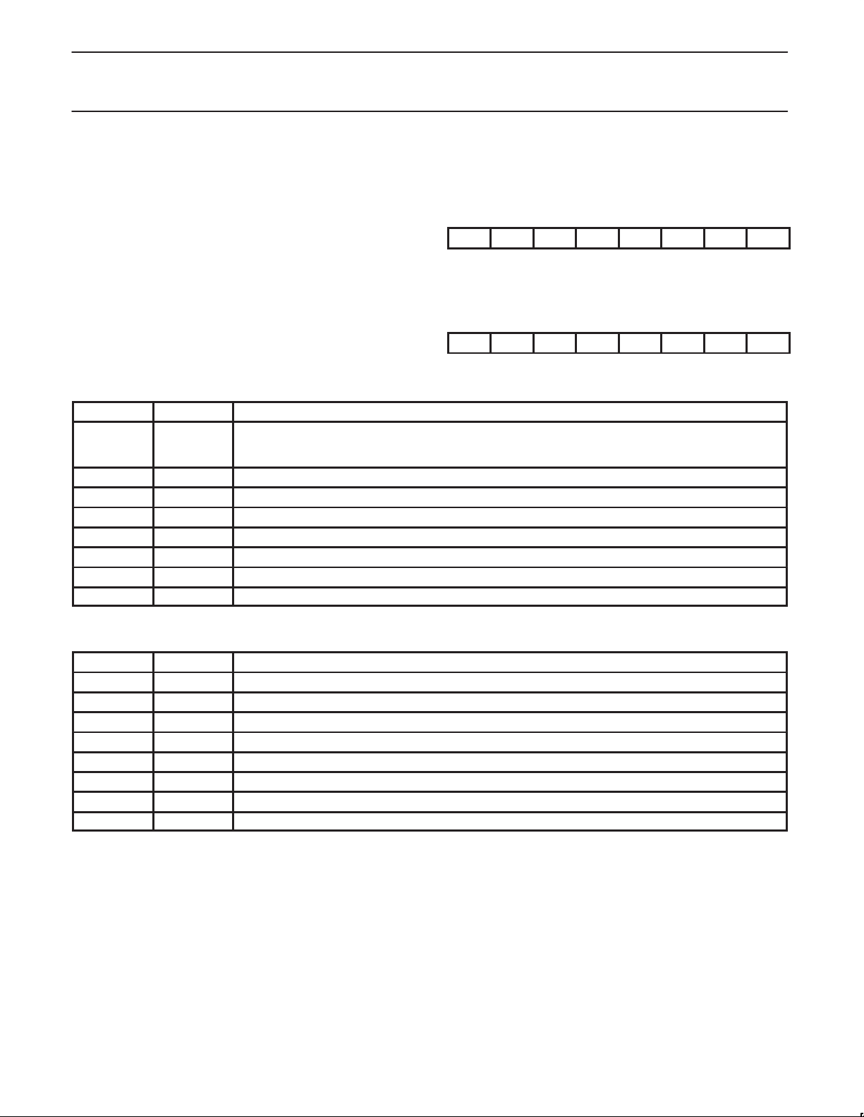
Table 3. Description of IE Bits
MNEMONIC BIT FUNCTION
EA IE.7 General enable/disable control:
ES1 IE.6 Enable bit-level I2C I/O interrupt
ET2 IE.5 Enable Timer 2 interrupt
ES IE.4 Enable Serial Port interrupt
ET1 IE.3 Enable Timer 1 interrupt
EX1 IE.2 Enable External interrupt 1
ET0 IE.1 Enable Timer 0 interrupt
EX0 IE.0 Enable External interrupt 0
C, watchdog timer
2
C interface: S1INT, S1BIT and
0 = NO interrupt is enabled.
1 = ANY individually enabled interrupt will be accepted.
87C524/87C528
IE: Interrupt Enable Register
This register is located at address A8H. Refer to Table 3.
IE SFR (A8H)
76543210
ES1 ET2 ES ET1 EX1 ET0 EX0
EA
IP: Interrupt Priority Register
This register is located at address B8H. Refer to Table 4.
IP SFR (B8H)
76543210
– PS1 PT2 PS PT1 PX1 PT0 PX0
Table 4. Description of IP Bits
MNEMONIC BIT FUNCTION
– IP.7 Reserved.
PS1 IP.6 Bit-level I2C interrupt priority level
PT2 IP .5 Timer 2 interrupt priority level
PS IP.4 Serial Port interrupt priority level
PT1 IP .3 Timer 1 interrupt priority level
PX1 IP.2 External Interrupt 1 priority level
PT0 IP.1 Timer 0 interrupt priority level
PX0 IP.0 External Interrupt 0 priority level
The interrupt vector locations and the interrupt priorities are:
Source Priority within Level
Vector Address
0003H IE0 Highest
002BH TF2+EXF2
0053H SI (I
000BH TF0
0013H IE1
001BH TF1
0023H RI+TI Lowest
2
C)
1999 Jul 23
9
Page 10
Philips Semiconductors Product specification
80C51 8-bit microcontrollers
2
16K/32K, 512 OTP, I
OSCILLA T OR CHARACTERISTICS
XTAL1 and XTAL2 are the input and output, respectively , of an
inverting amplifier . The pins can be configured for use as an on-chip
oscillator, as shown in the Logic Symbol.
To drive the device from an external clock source, XTAL1 should be
driven while XTAL2 is left unconnected. There are no requirements
on the duty cycle of the external clock signal, because the input to
the internal clock circuitry is through a divide-by-two flip-flop.
However, minimum and maximum high and low times specified in
the data sheet must be observed.
RESET
A reset is accomplished by holding the RST pin high for at least two
machine cycles (24 oscillator periods), while the oscillator is running.
To insure a good power-up reset, the RST pin must be high long
enough to allow the oscillator time to start up (normally a few
milliseconds) plus two machine cycles. At power-up, the voltage on
V
and RST must come up at the same time for a proper start-up.
DD
IDLE MODE
In idle mode, the CPU puts itself to sleep while all of the on-chip
peripherals stay active. The instruction to invoke the idle mode is the
last instruction executed in the normal operating mode before the
idle mode is activated. The CPU contents, the on-chip RAM, and all
of the special function registers remain intact during this mode. The
idle mode can be terminated either by any enabled interrupt (at
which time the process is picked up at the interrupt service routine
and continued), or by a hardware reset which starts the processor in
the same manner as a power-on reset.
C, watchdog timer
87C524/87C528
POWER-DOWN MODE
In the power-down mode, the oscillator is stopped and the
instruction to invoke power-down is the last instruction executed.
The power-down mode can be terminated by a RESET in the same
way as in the 80C51 or in addition by one of two external interrupts,
INT0 or INT1. A termination with an external interrupt does not affect
the internal data memory and does not affect the special function
registers. This makes it possible to exit power-down without
changing the port output levels. To terminate the power-down mode
with an external interrupt INT0
level-sensitive and must be enabled. The external interrupt input
signal INT0
restarted and stabilized. An instruction following the instruction that
puts the device in the power-down mode will be executed. A reset
generated by the watchdog timer terminates the power-down mode
in the same way as an external RESET, and only the contents of the
on-chip RAM are preserved. The control bits for the reduced power
modes are in the special function register PCON.
and INT1 must be kept low until the oscillator has
DESIGN CONSIDERATIONS
At power-on, the voltage on VDD and RST must come up at the
same time for a proper start-up.
When the idle mode is terminated by a hardware reset, the device
normally resumes program execution, from where it left off, up to
two machine cycles before the internal reset algorithm takes control.
On-chip hardware inhibits access to internal RAM in this event, but
access to the port pins is not inhibited. To eliminate the possibility of
an unexpected write when idle is terminated by reset, the instruction
following the one that invokes idle should not be one that writes to a
port pin or to external memory.
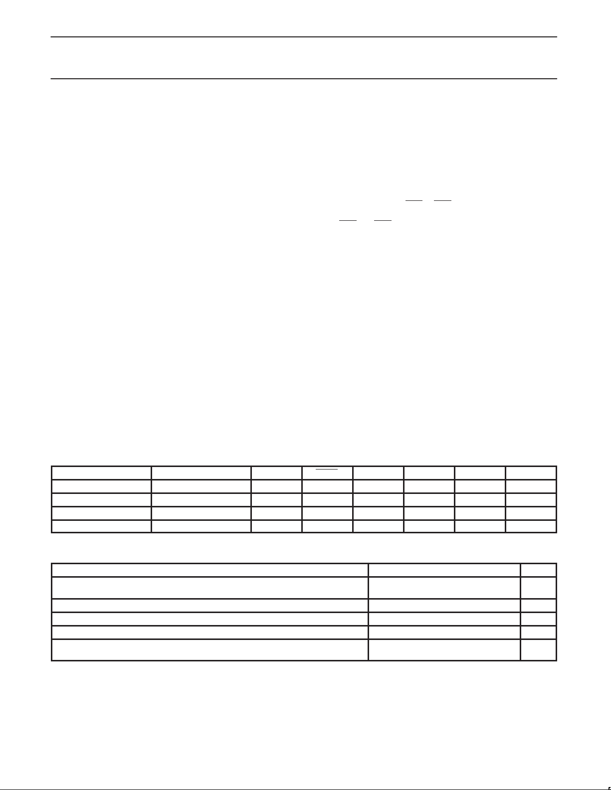
Table 5 shows the state of I/O ports during low current operating
modes.
or INT1 must be switched to
Table 5. External Pin Status During Idle and Power-Down Modes
MODE PROGRAM MEMORY ALE PSEN PORT 0 PORT 1 PORT 2 PORT 3
Idle Internal 1 1 Data Data Data Data
Idle External 1 1 Float Data Address Data
Power-down Internal 0 0 Data Data Data Data
Power-down External 0 0 Float Data Data Data
ABSOLUTE MAXIMUM RATINGS
Operating temperature under bias
Storage temperature range –65 to +150 °C
Voltage on any other pin to V
Input, output current on any two pins ±10 mA
Power dissipation
(based on package heat transfer limitations, not device power consumption)
NOTES:
1. Stresses above those listed under Absolute Maximum Ratings may cause permanent damage to the device. This is a stress rating only and
functional operation of the device at these or any conditions other than those described in the AC and DC Electrical Characteristics section
of this specification is not implied.
2. This product includes circuitry specifically designed for the protection of its internal devices from the damaging effects of excessive static
charge. Nonetheless, it is suggested that conventional precautions be taken to avoid applying greater than the rated maxima.
3. Parameters are valid over operating temperature range unless otherwise specified. All voltages are with respect to V
SS
1, 2, 3
PARAMETER
RATING UNIT
0 to +70, or
–40 to +85
–0.5 to VDD +0.5 V
1.0 W
unless otherwise noted.
SS
°C
1999 Jul 23
10
Page 11
Philips Semiconductors Product specification
80C51 8-bit microcontrollers
2
16K/32K, 512 OTP, I
C, watchdog timer
87C524/87C528
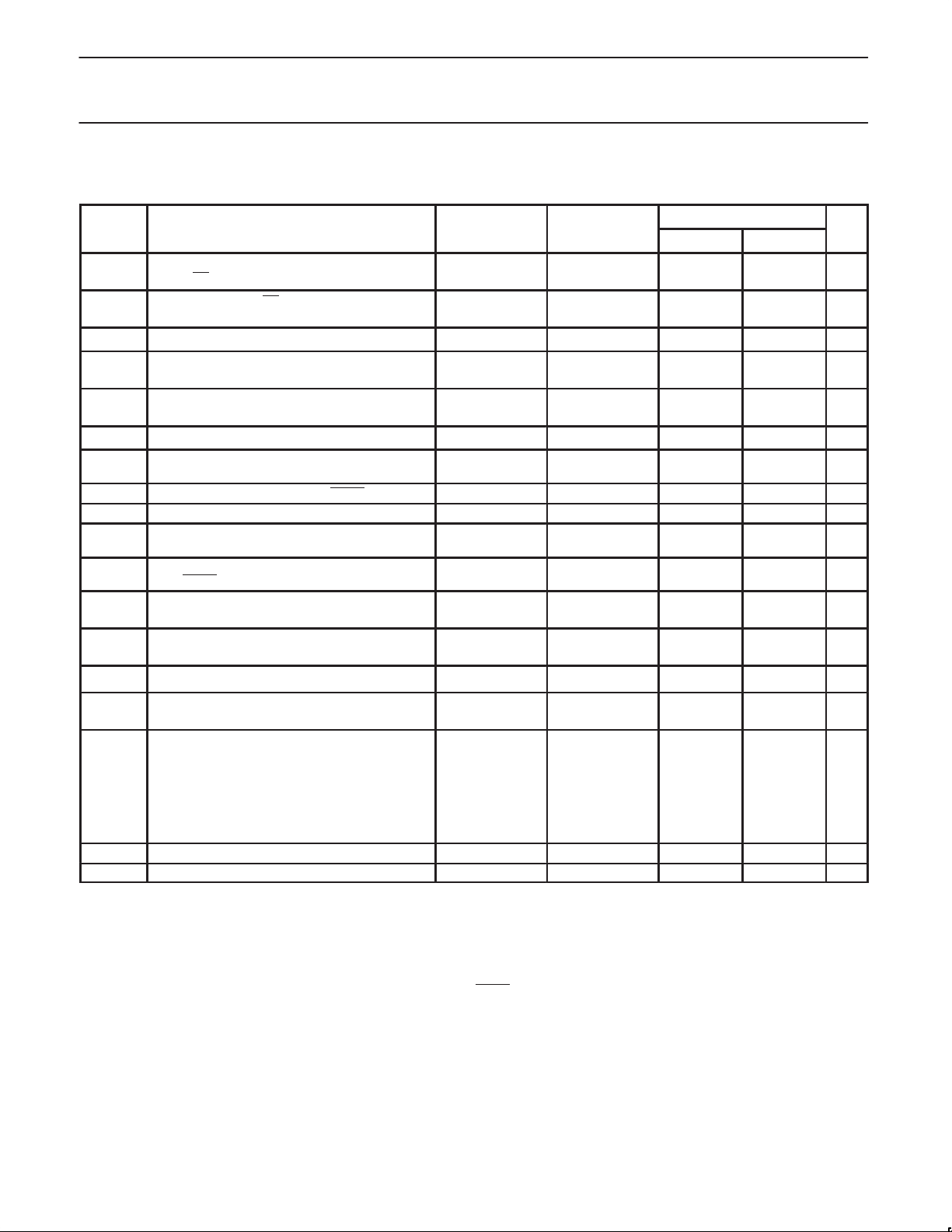
DC ELECTRICAL CHARACTERISTICS
T
= 0°C to +70°C (VDD = 5 V ±10%), –40°C to +85°C (VDD = 5 V ±10%), VSS=0 V
amb
TEST LIMITS
SYMBOL PARAMETER PART TYPE CONDITIONS MIN MAX UNIT
V
V
V
V
V
V
V
V
V
V
V
I
I
I
I
I
IL
IL1
IL2
IH
IH1
IH2
OL
OL1
OL2
OH
OH1
IL
TL
IL1
IL2
CC
Input low voltage,
except EA
, P1.6/SCL, P1.7/SDA
0°C to 70°C
–40°C to +85°C
Input low voltage to EA 0°C to 70°C
–40°C to +85°C
Input low voltage to P1.6/SCL, P1.7/SDA
Input high voltage,
except XTAL1, RST, P1.6/SCL, P1.7/SDA
5
0°C to 70°C
–40°C to +85°C
Input high voltage, XTAL1, RST 0°C to 70°C
–40°C to +85°C
Input high voltage, P1.6/SCL, P1.7/SDA
Output low voltage, ports 1, 2, 3, except
P1.6/SCL, P1.7/SDA
1
Output low voltage, port 0, ALE, PSEN
5
IOL = 1.6 mA
1
IOL = 3.2 mA
Output low voltage, P1.6/SCL, P1.7/SDA IOL = 3.0 mA
Output high voltage, ports 1, 2, 3 IOH = –60 µA
IOH = –25 µA
Output high voltage, Port 0 in external bus mode,
ALE, PSEN, RST
Logical 0 input current, ports 1, 2, 3,
except P1.6/SCL, P1.7/SDA
Logical 1-to-0 transition current, ports 1, 2, 3,
except P1.6/SCL, P1.7/SDA
0°C to 70°C
–40°C to +85°C
0°C to 70°C
–40°C to +85°C
IOH = –800 µA
IOH = –300 µA
VIN = 0.45 V –50
See Note 3 –650
Input leakage current, port 0 VIN = VIL or V
Input leakage current, P1.6/SCL, P1.7/SDA 0 V<Vi<6.0 V
0 V<VCC<6.0 V
Power supply current: See Note 4
1
1
1
IH
–0.5
–0.5
0
0
0.2VCC–0.1
0.2V
–0.15
CC
0.2VCC–0.3
0.2VCC–0.35VV
–0.5 0.3 V V
0.2VCC+0.9
0.2VCC+1.0
0.7V
CC
0.7VCC+0.1
VCC+0.5
VCC+0.5
VCC+0.5
VCC+0.5
3.0 6.0 V
0.45 V
0.45 V
0.4 V
2.4
0.75V
CC
2.4
0.75V
CC
–75
–750
±10
±10
V
V
V
V
V
V
V
V
V
V
µA
µA
µA
µA
µA
µA
µA
Active mode @ 16 MHz 0oC to 70oC
–40oC to +85oC
Idle mode @ 16 MHz 0oC to 70oC
–40oC to +85oC
25
35
5
6
Power down mode 50 µA
R
RST
C
IO
Internal reset pull-down resistor 50 300 kΩ
Pin Capacitance 10 pF
NOTES:
1. Capacitive loading on Port 0 and Port 2 may cause spurious noise pulses to be superimposed on the V
noise is due to external bus capacitance discharging into the port and port 2 pins when these pins make 1-to-0 transactions during bus
s of ALE and ports 1 and 3. The
OL
operations. In the worst cases (capacitive loading > 100pF), the noise pulse on the ALE pin may exceed 0.8V . In such cases, it may be
desirable to qualify ALE with a Schmitt Trigger, or use an address latch with a Schmitt Trigger STROBE input. Under steady state
(non-transient) conditions, I
(all bits) 15 mA.
2. Capacitive loading on Ports 0 and 2 may cause the V
address bits are stabilizing.
must be externally limited as follows: 10 mA per port pin, port 0 total (all bits) 26 mA, ports 1, 2, and total each
OL
on ALE and PSEN to momentarily fall below the 0.9VCC specification when the
OH
3. Pins of ports 1, 2, and 3 source a transition current when they are being externally driven from 1 to 0. The transition current reaches its
maximum value when V
4. See Figures 10 through 13 for I
5. The input threshold voltage of P1.6 and P1.7 (SIO1) meets the I
is approximately 2 V.
IN
test conditions.
CC
2
C specification, so an input voltage below 1.5 V will be recognized as a
logic 0 while an input voltage above 3.0 V will be recognized as a logic 1.
1999 Jul 23
11
mA
mA
Page 12
Philips Semiconductors Product specification
80C51 8-bit microcontrollers
2
16K/32K, 512 OTP, I
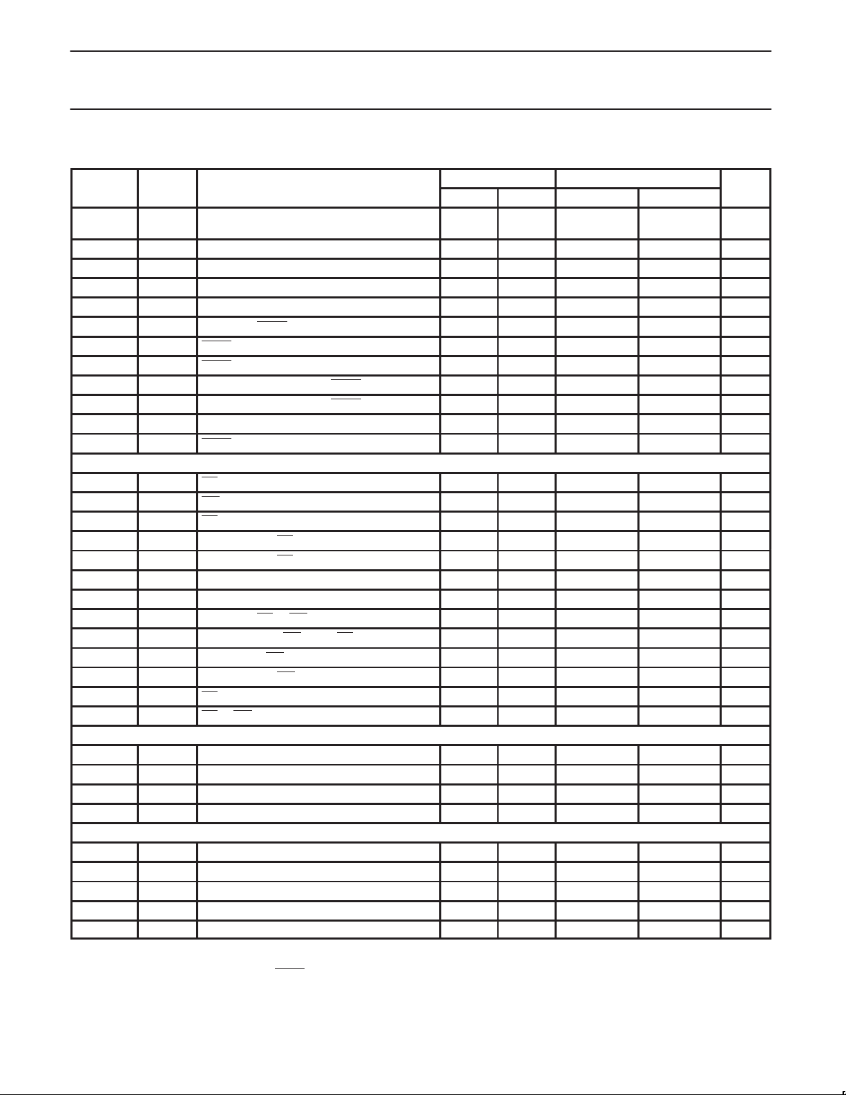
AC ELECTRICAL CHARACTERISTICS
C, watchdog timer
1, 2
87C524/87C528
16MHz CLOCK VARIABLE CLOCK
SYMBOL FIGURE PARAMETER MIN MAX MIN MAX UNIT
1/t
t
LHLL
t
AVLL
t
LLAX
t
LLIV
t
LLPL
t
PLPH
t
PLIV
t
PXIX
t
PXIZ
t
AVIV
t
PLAZ
CLCL
1 Oscillator frequency: Speed Versions
87C528 P878C528EXX 3.5 16 MHz
1 ALE pulse width 85 2t
1 Address valid to ALE low 8 t
1 Address hold after ALE low 28 t
1 ALE low to valid instruction in 150 4t
1 ALE low to PSEN low 23 t
1 PSEN pulse width 143 3t
1 PSEN low to valid instruction in 83 3t
–40 ns
CLCL
–55 ns
CLCL
–35 ns
CLCL
–100 ns
CLCL
–40 ns
CLCL
–45 ns
CLCL
–105 ns
CLCL
1 Input instruction hold after PSEN 0 0 ns
1 Input instruction float after PSEN 38 t
1 Address to valid instruction in 208 5t
–25 ns
CLCL
–105 ns
CLCL
1 PSEN low to address float 10 10 ns
Data Memory
t
RLRH
t
WLWH
t
RLDV
t
RHDX
t
RHDZ
t
LLDZ
t
AVDV
t
LLWL
t
AVWL
t
QVWX
t
WHQX
t
RLAZ
t
WHLH
2, 3 RD pulse width 275 6t
2, 3 WR pulse width 275 6t
2, 3 RD low to valid data in 148 5t
–100 ns
CLCL
–100 ns
CLCL
–165 ns
CLCL
2, 3 Data hold after RD 0 0 ns
2, 3 Data float after RD 55 2t
2, 3 ALE low to valid data in 350 8t
2, 3 Address to valid data in 398 9t
2, 3 ALE low to RD or WR low 138 238 3t
2, 3 Address valid to WR low or RD low 120 4t
2, 3 Data valid to WR transition 3 t
2, 3 Data hold after WR 13 t
–50 3t
CLCL
–130 ns
CLCL
–60 ns
CLCL
–50 ns
CLCL
–70 ns
CLCL
–150 ns
CLCL
–165 ns
CLCL
+50 ns
CLCL
2, 3 RD low to address float 0 0 ns
2, 3 RD or WR high to ALE high 23 103 t
–40 t
CLCL
+40 ns
CLCL
External Clock
t
CHCX
t
CLCX
t
CLCH
t
CHCL
6 High time 20 20 ns
6 Low time 20 20 ns
6 Rise time 20 20 ns
6 Fall time 20 20 ns
Shift Register
t
XLXL
t
QVXH
t
XHQX
t
XHDX
t
XHDV
4 Serial port clock cycle time 750 12t
4 Output data setup to clock rising edge 492 10t
4 Output data hold after clock rising edge 8 2t
CLCL
–133 ns
CLCL
–117 ns
CLCL
4 Input data hold after clock rising edge 0 0 ns
4 Clock rising edge to input data valid 492 10t
–133 ns
CLCL
NOTES:
1. Parameters are valid over operating temperature range unless otherwise specified.
2. Load capacitance for port 0, ALE, and PSEN
= 100pF, load capacitance for all other outputs = 80pF.
ns
1999 Jul 23
12
Page 13
Philips Semiconductors Product specification
80C51 8-bit microcontrollers
2
16K/32K, 512 OTP, I
C, watchdog timer
87C524/87C528
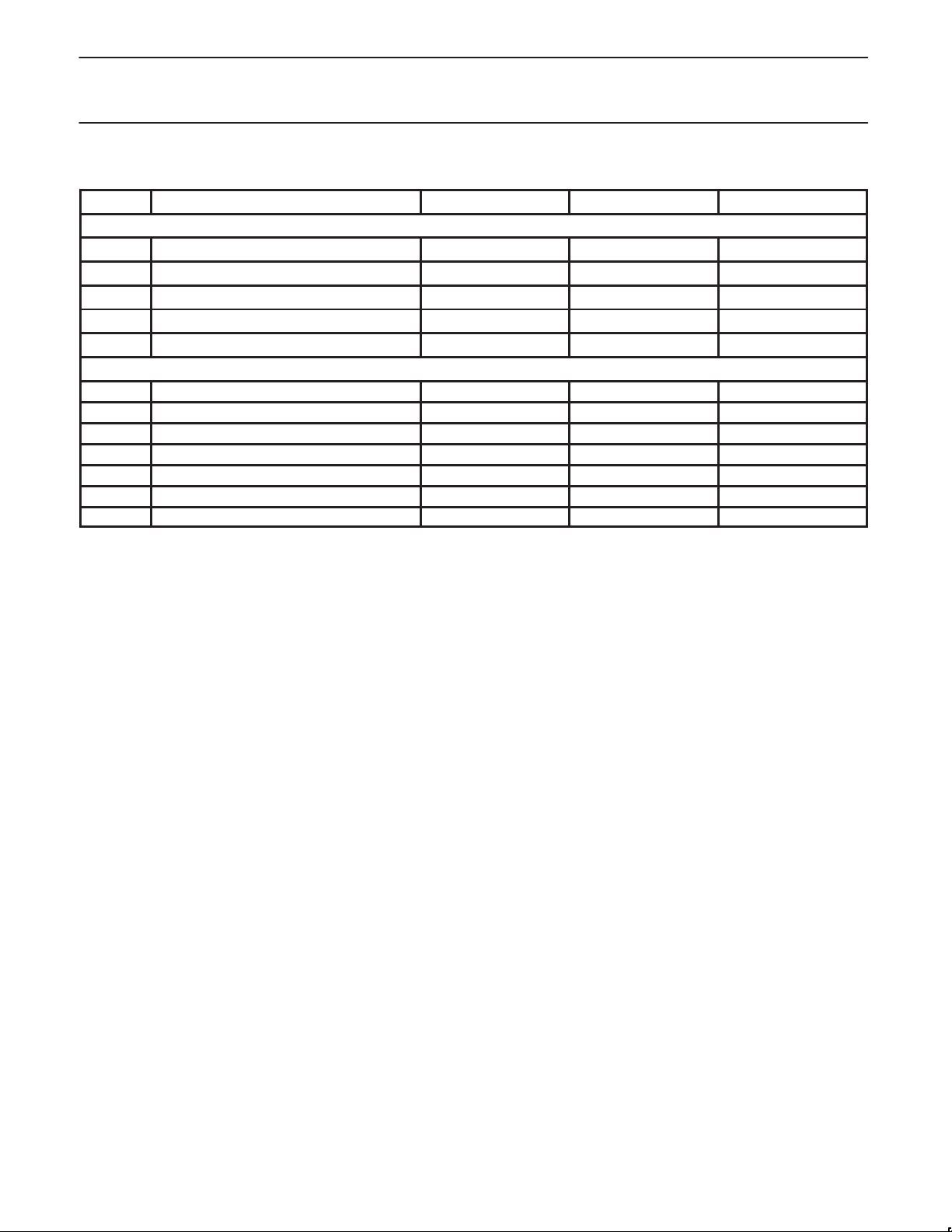
AC ELECTRICAL CHARACTERISTICS – I2C INTERFACE
SYMBOL PARAMETER INPUT OUTPUT I2C SPECIFICATION
SCL TIMING CHARACTERISTICS
t
HD;STA
t
LOW
t
HIGH
t
RC
t
FC
STAR T condition hold time ≥ 14 t
SCL LOW time ≥ 16 t
SCL HIGH time ≥ 14 t
SCL rise time ≤ 1µs
SCL fall time ≤ 0.3µs
SDA TIMING CHARACTERISTICS
t
SU;DAT1
t
HD;DAT
t
SU;STA
t
SU;STO
t
BUF
t
RD
t
FD
Data set-up time ≥ 250ns Note 2 ≥ 250ns
Data hold time ≥ 0ns Note 2 ≥ 0ns
Repeated START set-up time ≥ 14 t
STOP condition set-up time ≥ 14 t
Bus free time ≥ 14 t
SDA rise time ≤ 1µs
SDA fall time ≤ 0.3µs
NOTES:
1. At f
2. This parameter is determined by the user software, it has to comply with the I
3. This value gives the autoclock pulse length which meets the I
= 3.5MHz, this evaluates to 14 × 286ns = 4µs, i.e., the bit-level I2C interface can respond to the I2C protocol for f
CLK
2
C specification for the specified XTAL clock frequency range. Alternatively, the
SCL pulse may be timed by software.
4. Spikes on SDA and SCL lines with a duration of less than 4 × f
will be filtered out.
CLK
5. The rise time is determined by the external bus line capacitance and pull-up resistor, it must be ≤ 1µs.
6. The maximum capacitance on bus lines SDA and SCL is 400pF.
CLCL
CLCL
CLCL
1
CLCL
CLCL
CLCL
4
1
Note 2 ≥ 4.0µs
Note 2 ≥ 4.7µs
1
≥ 80 t
CLCL
3
≥ 4.0µs
Note 5 ≤ 1.0µs
1
1
1
1
6
≤ 0.3µs
≤ 0.3µs
Note 2 ≥ 4.7µs
Note 2 ≥ 4.0µs
Note 2 ≥ 4.7µs
Note 5 ≤ 1.0µs
4
2
C.
≤ 0.3µs
6
≤ 0.3µs
≥ 3.5 MHz.
CLK
1999 Jul 23
13
Page 14
Philips Semiconductors Product specification
80C51 8-bit microcontrollers
2
16K/32K, 512 OTP, I
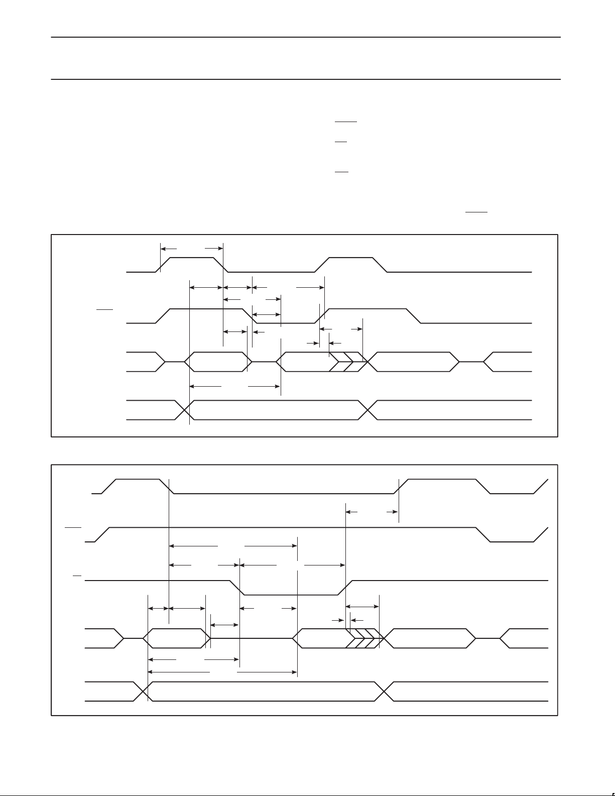
EXPLANATION OF THE AC SYMBOLS
Each timing symbol has five characters. The first character is always
‘t’ (= time). The other characters, depending on their positions,
indicate the name of a signal or the logical status of that signal. The
designations are:
A – Address
C – Clock
D – Input data
H – Logic level high
I – Instruction (program memory contents)
L – Logic level low, or ALE
ALE
PSEN
PORT 0
C, watchdog timer
t
LHLL
t
t
AVLL
LLPL
t
LLAX
A0–A7 A0–A7
t
LLIV
t
PLIV
t
PLPH
t
PLAZ
t
PXIX
P – PSEN
Q – Output data
R–RD
signal
t – Time
V – Valid
W– WR
signal
X – No longer a valid logic level
Z – Float
Examples: t
INSTR IN
t
PXIZ
AVLL
t
LLPL
87C524/87C528
= Time for address valid to ALE low.
= Time for ALE low to PSEN low.
ALE
PSEN
PORT 0
PORT 2
RD
PORT 2
t
AVLL
t
LLAX
A0–A7
FROM RI OR DPL
t
AVWL
t
AVIV
A0–A15 A8–A15
Figure 1. External Program Memory Read Cycle
t
WHLH
t
LLDV
t
LLWL
t
RLAZ
t
AVDV
P2.0–P2.7 OR A8–A15 FROM DPH A0–A15 FROM PCH
t
RLDV
t
RLRH
t
RHDZ
t
RHDX
DATA IN A0–A7 FROM PCL INSTR IN
SU00006
1999 Jul 23
SU00007
Figure 2. External Data Memory Read Cycle
14
Page 15
Philips Semiconductors Product specification
80C51 8-bit microcontrollers
2
16K/32K, 512 OTP, I
ALE
PSEN
WR
t
AVLL
PORT 0
PORT 2
FROM RI OR DPL
C, watchdog timer
t
LLWL
t
LLAX
A0–A7
t
AVWL
P2.0–P2.7 OR A8–A15 FROM DPF A0–A15 FROM PCH
87C524/87C528
t
WHLH
t
WLWH
t
t
QVWX
DATA OUT A0–A7 FROM PCL INSTR IN
WHQX
INSTRUCTION
ALE
CLOCK
OUTPUT DATA
WRITE TO SBUF
INPUT DATA
CLEAR RI
SU00069
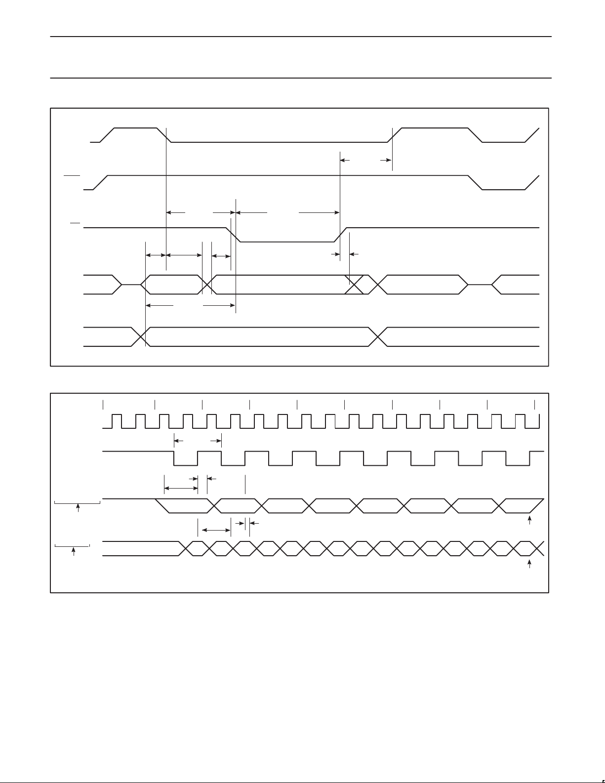
Figure 3. External Data Memory Write Cycle
012345678
t
XLXL
t
t
QVXH
t
XHDV
VALID VALID VALID VALID VALID VALID VALID VALID
XHQX
1230 4567
t
XHDX
SET TI
SET RI
SU00027
Figure 4. Shift Register Mode Timing
1999 Jul 23
15
Page 16
Philips Semiconductors Product specification
80C51 8-bit microcontrollers
2
16K/32K, 512 OTP, I
START or repeated START condition
SDA
(INPUT/OUTPUT)
t
FDtRC
SCL
(INPUT/OUTPUT)
t
HD;STA
t
C, watchdog timer
t
RD
t
LOW
HIGH
VCC–0.5
0.45V
repeated START condition
STOP condition
t
FC
t
SU;DAT1
t
HD;DAT
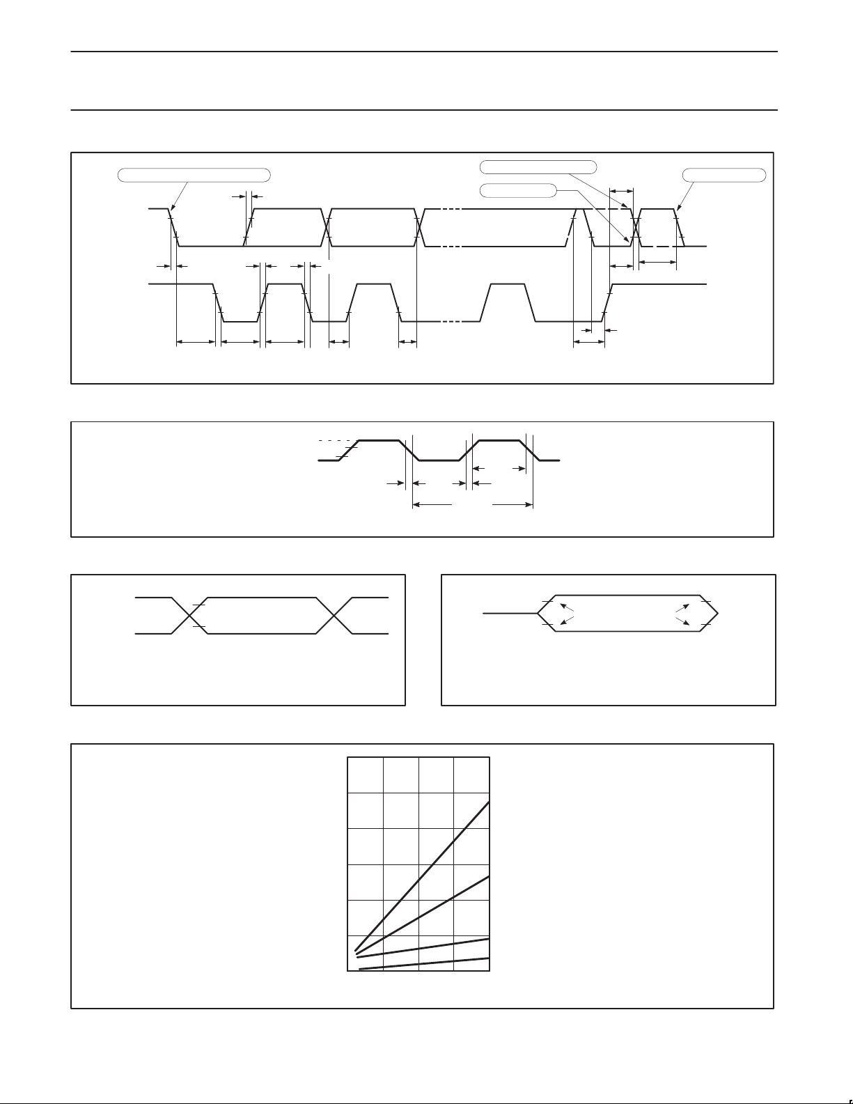
Figure 5. Timing SIO1 (I2C) Interface
0.7V
CC
0.2VCC–0.1
t
CHCL
t
CLCX
t
CLCL
t
CHCX
t
CLCH
Figure 6. External Clock Drive
SU00009
87C524/87C528
t
SU;STA
t
BUF
t
SU;STO
0.7 V
CC
0.3 V
CC
t
SU;DAT3
t
SU;DAT2
START condition
0.7 V
CC
0.3 V
CC
SU00107A
VDD–0.5
0.45V
NOTE:
AC inputs during testing are driven at VDD –0.5 for a logic ‘1’ and 0.45V for a logic ‘0’.
Timing measurements are made at V
+0.9
0.2V
DD
0.2VDD–0.1
min for a logic ‘1’ and VIL max for a logic ‘0’.
IH
SU00167
Figure 7. AC Testing Input/Output
30
25
20
15
mA
I
CC
10
5
4 MHz 8 MHz 12 MHz 16 MHz
Figure 9. ICC vs. FREQ.
Valid only within frequency specifications of the device under test
FREQ AT XTAL1
V
+0.1V
LOAD
V
LOAD
V
–0.1V
LOAD
NOTE:
For timing purposes, a port is no longer floating when a 100mV change from load
voltage occurs, and begins to float when a 100mV change from the loaded V
level occurs. IOH/IOL ≥ ±20mA.
TIMING
REFERENCE
POINTS
V
OH
V
OL
–0.1V
+0.1V
OH/VOL
SU00011
Figure 8. Float Waveform
MAX ACTIVE MODE
TYP ACTIVE MODE
MAX IDLE MODE
TYP IDLE MODE
SU00168
1999 Jul 23
16
Page 17
Philips Semiconductors Product specification
80C51 8-bit microcontrollers
2
16K/32K, 512 OTP, I
V
DD
RST
(NC)
CLOCK SIGNAL
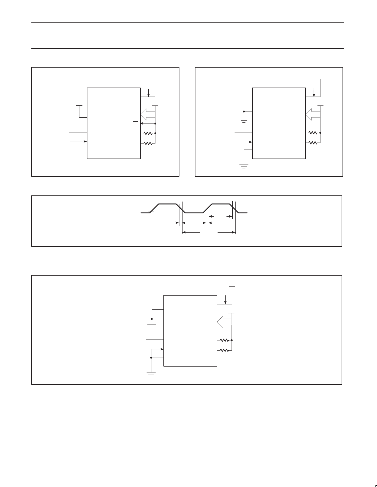
Figure 10. IDD Test Condition, Active Mode
All other pins are disconnected
XTAL2
XTAL1
V
SS
C, watchdog timer
V
DD
P0
EA
P1.6
P1.7
VCC–0.5
0.45V
V
DD
I
DD
V
DD
(NC)
SU00169
*
*
CLOCK SIGNAL
Figure 11. IDD Test Condition, Idle Mode
0.7V
CC
0.2VCC–0.1
t
CHCL
t
CLCX
t
CLCL
t
CHCX
t
CLCH
Figure 12. Clock Signal Waveform for
I
Tests in Active and Idle Modes
DD
t
CLCH
= t
CHCL
= 5ns
87C524/87C528
V
RST
EA
XTAL2
XTAL1
V
SS
All other pins are disconnected
SU00009
DD
P0
P1.6
P1.7
V
DD
I
DD
V
DD
SU00170
*
*
NOTE:
* Ports 1.6 and 1.7 should be connected to V
exceed the I
specifications.
OL1
V
DD
I
DD
V
(NC)
RST
EA
XTAL2
XTAL1
V
SS
P1.6
P1.7
DD
V
DD
P0
*
*
SU00171
Figure 13. IDD Test Condition, Power Down Mode
All other pins are disconnected. V
through resistors of sufficiently high value such that the sink current into these pins does not
DD
= 2V to 5.5V
DD
1999 Jul 23
17
Page 18
Philips Semiconductors Product specification
80C51 8-bit microcontrollers
2
16K/32K, 512 OTP, I
EPROM CHARACTERISTICS FOR 87C528
The 87C528 is programmed by using a modified Quick-Pulse
Programming algorithm. It differs from older methods in the value
used for V
number of the ALE/PROG
The 87C528 contains two signature bytes that can be read and used
by an EPROM programming system to identify the device. The
signature bytes identify the device as an 87C528 manufactured by
Philips.
Table 6 shows the logic levels for reading the signature byte, and for
programming the program memory, the encryption table, and the
lock bits. The circuit configuration and waveforms for quick-pulse
programming are shown in Figures 14 and 15. Figure 16 shows the
circuit configuration for normal program memory verification.
Quick-Pulse Programming
The setup for microcontroller quick-pulse programming is shown in
Figure 14. Note that the 87C528 is running with a 4 to 6MHz
oscillator The reason the oscillator needs to be running is that the
device is executing internal address and program data transfers.
The address of the EPROM location to be programmed is applied to
ports 1, 2 and 3, as shown in Figure 14. The code byte to be
programmed into that location is applied to port 0. RST, PSEN
pins of ports 2 and 3 specified in Table 6 are held at the ’Program
Code Data’ levels indicated in Table 6. The ALE/PROG
low 25 times as shown in Figure 15.
To program the encryption table, repeat the 25 pulse programming
sequence for addresses 0 through 3FH, using the ‘Pgm Encryption
Table’ levels. Do not forget that after the encryption table is
programmed, verification cycles will produce only encrypted data.
To program the lock bits, repeat the 25 pulse programming
sequence using the ‘Pgm Lock Bit’ levels. After one lock bit is
programmed, further programming of the code memory and
encryption table is disabled. However, the other lock bit can still be
programmed.
(programming supply voltage) and in the width and
PP
pulses.
C, watchdog timer
and
is pulsed
87C524/87C528
Note that the EA
maximum specified V
glitch above that voltage can cause permanent damage to the
device. The V
and overshoot.
Program Verification
If lock bit 2 has not been programmed, the on-chip program memory
can be read out for program verification. The address of the program
memory locations to be read is applied to ports 1, 2 and 3 as shown
in Figure 16. The other pins are held at the ‘Verify Code Data’ levels
indicated in Table 6. The contents of the address location will be
emitted on port 0. External pull ups are required on port 0 for this
operation.
If the encryption table has been programmed, the data presented at
port 0 will be the exclusive NOR of the program byte with one of the
encryption bytes. The user will have to know the encryption table
contents in order to correctly decode the verification data. The
encryption table itself cannot be read out.
Reading the Signature Bytes
The signature bytes are read by the same procedure as a normal
verification of locations 030H and 031 H, except that P3.6 and P3.7
need to be pulled to a logic low. The values are:
(030H) = 15H indicates manufactured by Philips
(031H) = 9BH indicates 87C528
Program Lock Bits
The 87C528 has 3 programmable lock bits that will provide different
levels of protection for the on-chip code and data (see Table 7).
Erasing the EPROM also erases the encryption array and the
program lock bits, returning the part to full functionality.
Program/Verify Algorithms
Any algorithm in agreement with the conditions listed in Table 6, and
which satisfies the timing specifications, is suitable.
/VPP pin must not be allowed to 90 above the
level for any amount of time. Even a narrow
PP
source should be well regulated and free of glitches
PP
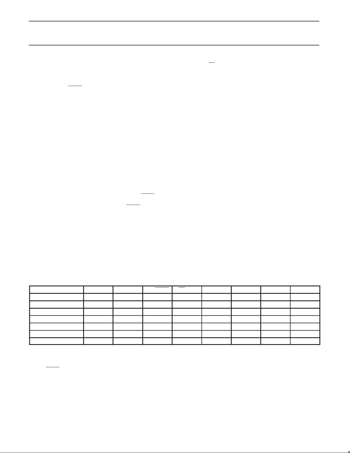
Table 6. EPROM Programming Modes
MODE RST PSEN ALE/PROG EA/V
Read signature 1 0 1 1 0 0 0 0
Program code data 1 0 0* V
Verify code data 1 0 1 1 0 0 1 1
Pgm encryption table 1 0 0* V
Pgm lock bit 1 1 0 0* V
Pgm lock bit 2 1 0 0* V
Pgm lock bit 3 1 0 0* V
NOTES:
1. ‘0’ = V alid low for that pin, ‘1’ = valid high for that pin.
2. V
= 12.75 V ±0.25 V .
PP
3. Vcc = 5 V ±10% during programming and verification.
* ALE/PROG
minimum of 10 µs.
1999 Jul 23
receives 25 programming pulses while VPP is held at 12.75 V. Each programming pulse is low for 100 µs (±10 µs) and high for a
18
PP
PP
PP
PP
PP
PP
P2.7 P2.6 P3.7 P3.6
1 0 1 1
1 0 1 0
1 1 1 1
1 1 0 0
0 1 0 1
Page 19

Philips Semiconductors Product specification
80C51 8-bit microcontrollers
2
16K/32K, 512 OTP, I
EPROM CHARACTERISTICS FOR 87C524
The 87C524 is programmed by using a modified Quick-Pulse
Programming algorithm. It differs from older methods in the value
used for V
number of the ALE/PROG
The 87C524 contains two signature bytes that can be read and used
by an EPROM programming system to identify the device. The
signature bytes identify the device as an 87C524 manufactured by
Philips.
Table 6 shows the logic levels for reading the signature byte, and for
programming the program memory, the encryption table, and the
lock bits. The circuit configuration and waveforms for quick-pulse
programming are shown in Figures 14 and 15. Figure 16 shows the
circuit configuration for normal program memory verification.
Quick-Pulse Programming
The setup for microcontroller quick-pulse programming is shown in
Figure 14. Note that the 87C524 is running with a 4 to 6 MHz
oscillator. The reason the oscillator needs to be running is that the
device is executing internal address and program data transfers.
The address of the EPROM location to be programmed is applied to
ports 1, 2 and 3, as shown in Figure 14. The code byte to be
programmed into that location is applied to port 0. RST, PSEN
pins of ports 2 and 3 specified in Table 6 are held at the ‘Program
Code Data’ levels indicated in Table 6. The ALE/PROG
low 25 times as shown in Figure 15.
To program the encryption table, repeat the 25 pulse programming
sequence for addresses 0 through 3FH, using the ‘Pgm Encryption
Table’ levels. Do not forget that after the encryption table is
programmed, verification cycles will produce only encrypted data.
To program the lock bits, repeat the 25 pulse programming
sequence using the ‘Pgm Lock Bit’ levels. After one lock bit is
programmed, further programming of the code memory and
encryption table is disabled. However, the other lock bit can still be
programmed.
Note that the EA
maximum specified V
glitch above that voltage can cause permanent damage to the
device. The V
and overshoot.
Program Verification
If lock bit 2 has not been programmed, the on-chip program memory
can be read out for program verification. The address of the program
memory locations to be read is applied to ports 1, 2 and 3 as shown
(programming supply voltage) and in the width and
PP
/VPP pin must not be allowed to go above the
source should be well regulated and free of glitches
PP
pulses.
level for any amount of time. Even a narrow
PP
C, watchdog timer
and
is pulsed
87C524/87C528
in Figure 16. The other pins are held at the ‘Verify Code Data’ levels
indicated in Table 6. The contents of the address location will be
emitted on port 0. External pull-ups are required on port 0 for this
operation.
If the encryption table has been programmed, the data presented at
port 0 will be the exclusive NOR of the program byte with one of the
encryption bytes. The user will have to know the encryption table
contents in order to correctly decode the verification data. The
encryption table itself cannot be read out.
Program Lock Bits
The 87C524 has 3 programmable lock bits that will provide different
levels of protection for the on-chip code and data (see Table 7).
Erasing the EPROM also erases the encryption array and the
program lock bits, returning the part to full functionality.
Reading the Signature Bytes
The signature bytes are read by the same procedure as a normal
verification of locations 030H and 031H, except that P3.6 and P3.7
need to be pulled to a logic low. The values are:
(030H) = 15H indicates manufactured by
(031H) = 9DH indicates 87C524
Program/Verify Algorithms
Any algorithm in agreement with the conditions listed in Table 6, and
which satisfies the timing specifications, is suitable.
Erasure Characteristics
Erasure of the EPROM begins to occur when the chip is exposed to
light with wavelengths shorter than approximately 4,000 angstroms.
Since sunlight and fluorescent lighting have wavelengths in this
range, exposure to these light sources over an extended time (about
1 week in sunlight, or 3 years in room level fluorescent lighting)
could cause inadvertent erasure. For this and secondary effects,
it is recommended that an opaque label be placed over the
window. For elevated temperature or environments where solvents
are being used, apply Kapton tape Fluorglas part number 2345–5, or
equivalent.
The recommended erasure procedure is exposure to ultraviolet light
(at 2537 angstroms) to an integrated dose of at least 15W-sec/cm2.
Exposing the EPROM to an ultraviolet lamp of 12,000uW/cm
for 20 to 39 minutes, at a distance of about 1 inch, should be
sufficient.
Erasure leaves the array in an all 1s state.
Philips
2
rating
Trademark phrase of Intel Corporation.
1999 Jul 23
19
Page 20
Philips Semiconductors Product specification
80C51 8-bit microcontrollers
2
16K/32K, 512 OTP, I
C, watchdog timer
87C524/87C528
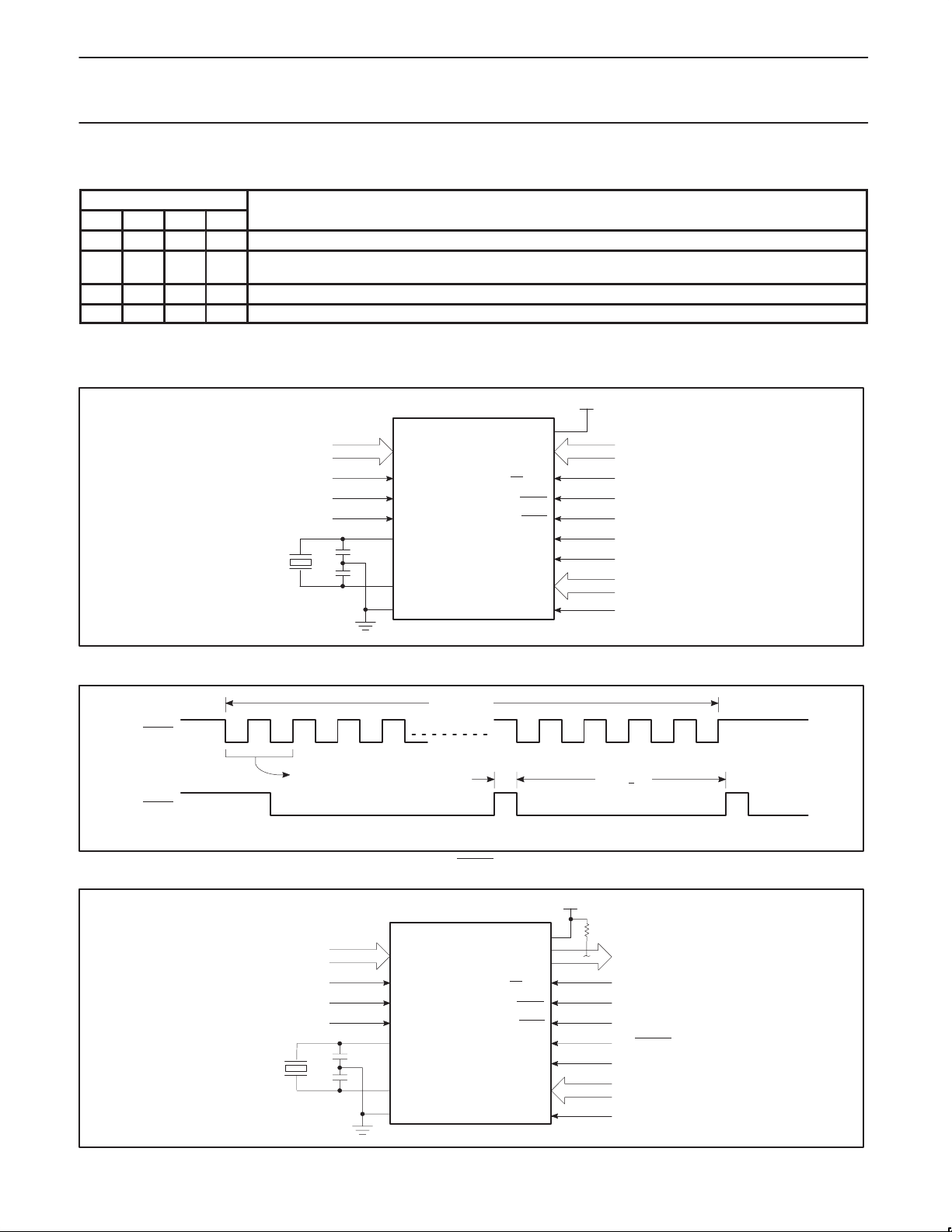
Table 7. Program Lock Bits
PROGRAM LOCK BITS
LB1 LB2 LB3 PROTECTION DESCRIPTION
1 U U U No Program Lock features enabled. (Code verify will still be encrypted by the Encryption Array if programmed.)
2 P U U MOVC instructions executed from external program memory are disabled from fetching code bytes from
3 P P U Same as 2, also verify is disabled.
4 P P P Same as 3, external execution is disabled. Internal data RAM is not accessible.
NOTES:
1. P - programmed. U - unprogrammed.
2. Any other combination of the lock bits is not defined.
1,2
Internal memory , EA is jumped and latched on Reset, and further programming of the EPROM Is disabled.
+5 V
V
CC
P0
EA/V
PP
ALE/PROG
PSEN
P2.7
P2.6
P2.0–P2.5
P3.4
PGM DATA
+12.75 V
25 100 µs PULSES TO GROUND
0
1
0
A8–A13
A14
SU00172
4–6 MHz
A0–A7
P1
1
1
1
RST
P3.6
P3.7
XTAL2
XTAL1
V
SS
87C524/8
Figure 14. Programming Configuration
ALE/PROG:
ALE/PROG:
1
0
1
0
25 PULSES
100µs+1010µs MIN
SU00018
Figure 15. PROG Waveform
+5 V
V
CC
/V
EA
PP
ALE/PROG
PSEN
P2.7
P2.6
P2.0–P2.5
P3.4
P0
PGM DATA
1
1
0
0 ENABLE
0
A8–A13
A14
SU00173
4–6 MHz
A0–A7
P1
1
1
1
RST
P3.6
P3.7
XTAL2
XTAL1
V
SS
87C524/8
Figure 16. Program Verification
1999 Jul 23
20
Page 21
Philips Semiconductors Product specification
80C51 8-bit microcontrollers
2
16K/32K, 512 OTP, I
C, watchdog timer
87C524/87C528
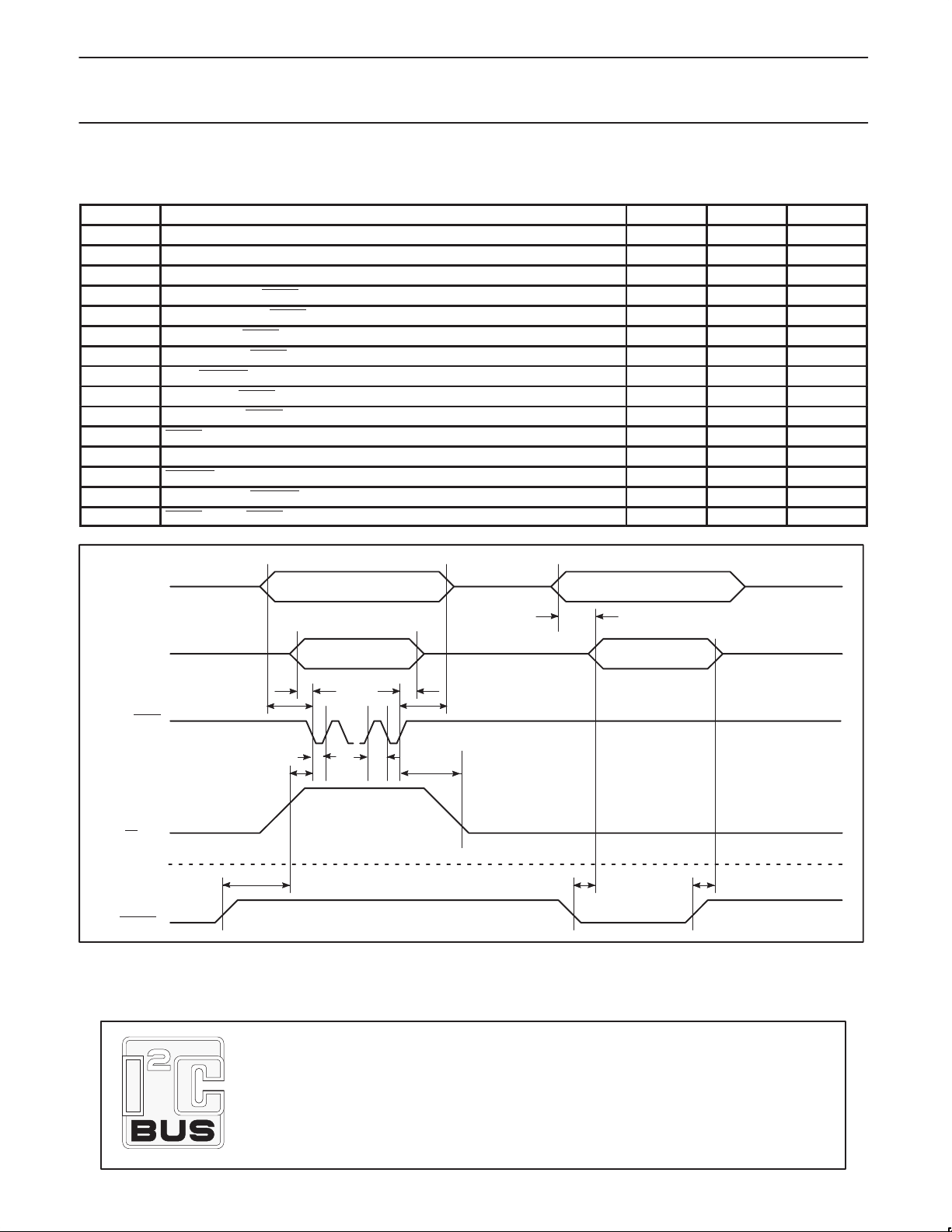
EPROM PROGRAMMING AND VERIFICATION CHARACTERISTICS
T
= 21°C to +27°C, Vcc = 5 V±10%, VSS = 0 V (See Figure 17)
amb
SYMBOL PARAMETER MIN MAX UNIT
V
1/t
t
AVGL
t
GHAX
t
DVGL
t
GHDX
t
EHSH
t
SHGL
t
GHSL
t
GLGH
t
AVQV
t
ELQZ
t
EHQZ
t
GHGL
PP
I
PP
CLCL
Programming supply voltage 12.5 13.0 V
Programming supply current 50 mA
Oscillator frequency 4 6 MHz
Address setup to PROG low 48t
Address hold after PROG 48t
Data setup to PROG low 48t
Data hold after PROG 48t
P2.7 (ENABLE) high to V
PP
48t
CLCL
CLCL
CLCL
CLCL
CLCL
VPP setup to PROG low 10 µs
VPP hold after PROG 10 µs
PROG width 90 110 µs
Address to data valid 48t
ENABLE low to data valid 48t
Data float after ENABLE 0 48t
CLCL
CLCL
CLCL
PROG high to PROG low 10 µs
PROGRAMMING* VERIFICATION*
P1.0–P1.7
P2.0–P2.5
PORT 0
t
DVGL
t
ALE/PROG
EA/V
PP
P2.7
ENABLE
NOTE:
* FOR PROGRAMMING VERIFICATION SEE FIGURE 14.
FOR VERIFICATION CONDITIONS SEE FIGURE 16.
AVGL
t
GLGH
t
SHGL
t
EHSH
ADDRESS ADDRESS
t
AVQV
DATA IN DATA OUT
t
GHDX
t
GHAX
t
GHGL
t
GHSL
LOGIC 1 LOGIC 1
LOGIC 0
t
ELQV
Figure 17. EPROM Programing and Verification
t
EHQZ
SU00174
1999 Jul 23
Purchase of Philips I2C components conveys a license under the Philips’ I2C patent
to use the components in the I2C system provided the system conforms to the
I2C specifications defined by Philips. This specification can be ordered using the
code 9398 393 40011.
21
Page 22
Philips Semiconductors Product specification
80C51 8-bit microcontrollers
2
16K/32K, 512 OTP, I
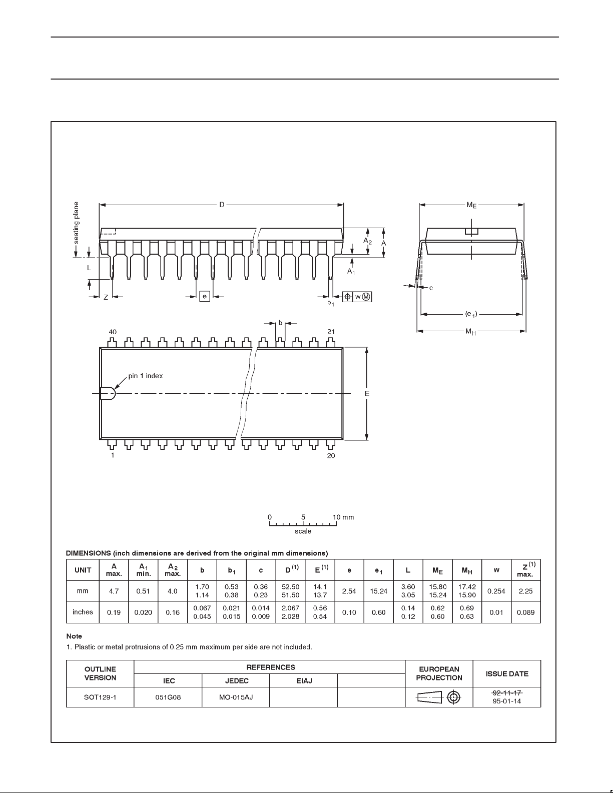
DIP40: plastic dual in-line package; 40 leads (600 mil) SOT129-1
C, watchdog timer
87C524/87C528
1999 Jul 23
22
Page 23
Philips Semiconductors Product specification
80C51 8-bit microcontrollers
2
16K/32K, 512 OTP, I
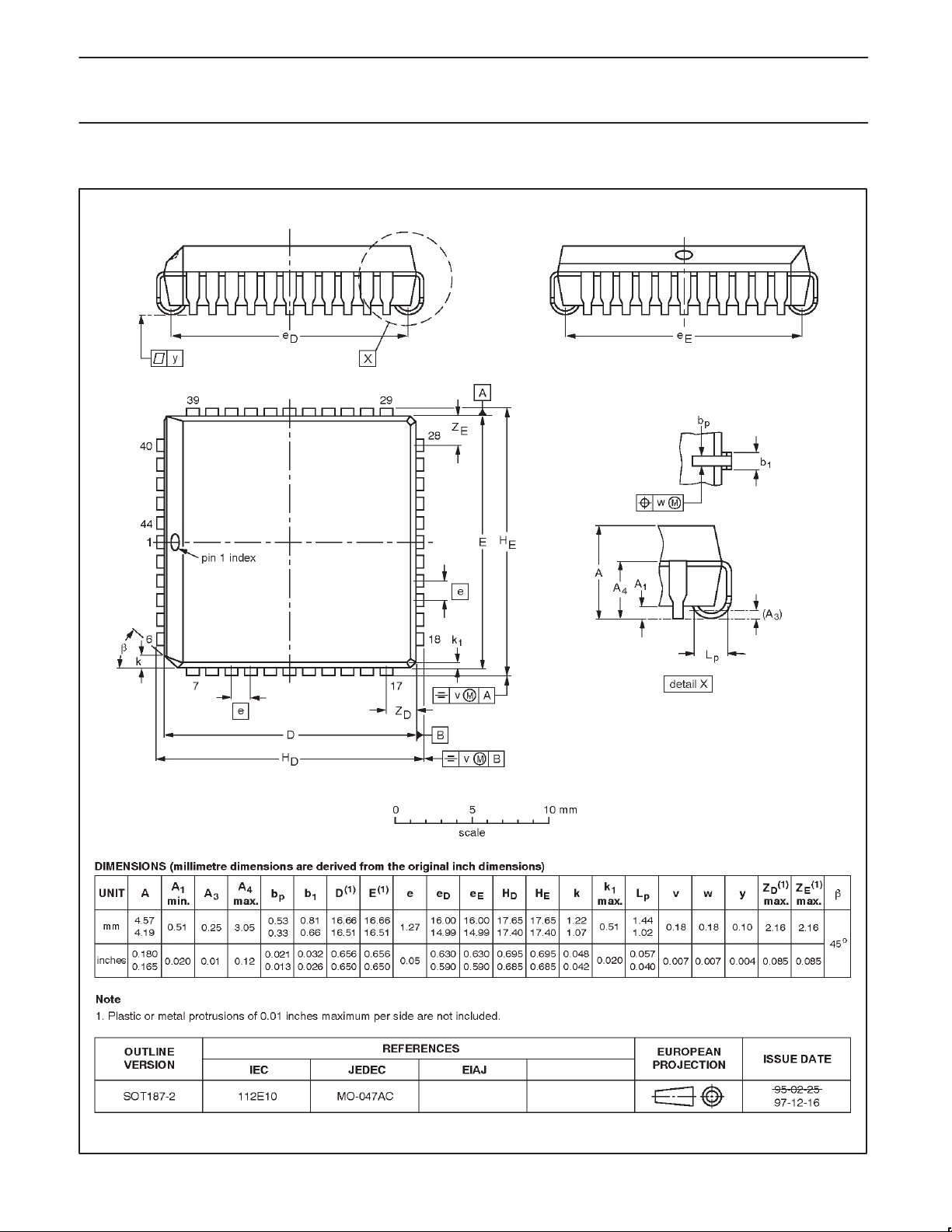
PLCC44: plastic leaded chip carrier; 44 leads SOT187-2
C, watchdog timer
87C524/87C528
1999 Jul 23
23
Page 24
Philips Semiconductors Product specification
80C51 8-bit microcontrollers
2
16K/32K, 512 OTP, I
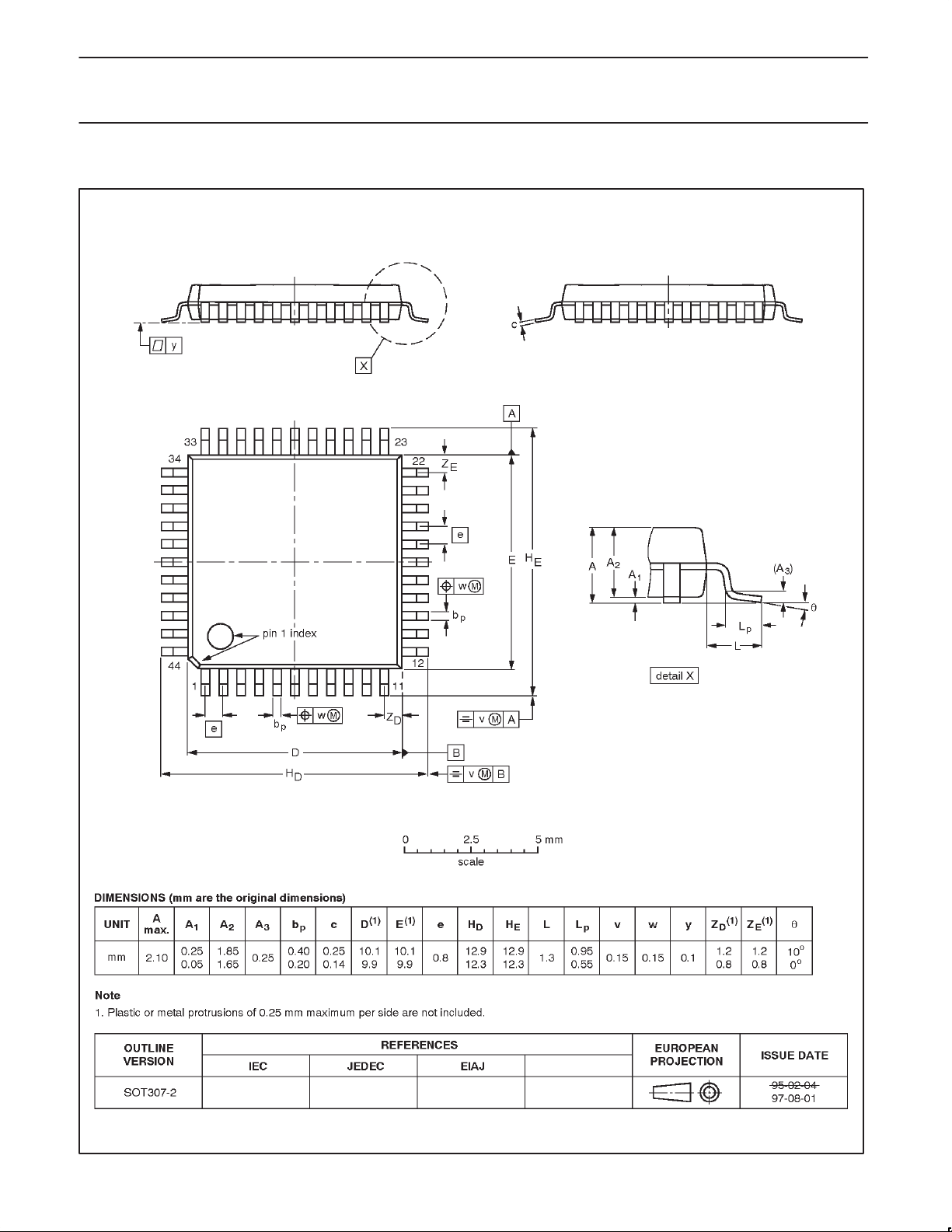
QFP44: plastic quad flat package; 44 leads (lead length 1.3 mm); body 10 x 10 x 1.75 mm SOT307-2
C, watchdog timer
87C524/87C528
1999 Jul 23
24
Page 25

Philips Semiconductors Product specification
80C51 8-bit microcontrollers
2
16K/32K, 512 OTP, I
C, watchdog timer
87C524/87C528
NOTES
1999 Jul 23
25
Page 26

Philips Semiconductors Product specification
80C51 8-bit microcontrollers
2
16K/32K, 512 OTP, I
Data sheet status
Data sheet
status
Objective
specification
Preliminary
specification
Product
specification
Product
status
Development
Qualification
Production
C, watchdog timer
Definition
This data sheet contains the design target or goal specifications for product development.
Specification may change in any manner without notice.
This data sheet contains preliminary data, and supplementary data will be published at a later date.
Philips Semiconductors reserves the right to make changes at any time without notice in order to
improve design and supply the best possible product.
This data sheet contains final specifications. Philips Semiconductors reserves the right to make
changes at any time without notice in order to improve design and supply the best possible product.
87C524/87C528
[1]
[1] Please consult the most recently issued datasheet before initiating or completing a design.
Definitions
Short-form specification — The data in a short-form specification is extracted from a full data sheet with the same type number and title. For
detailed information see the relevant data sheet or data handbook.
Limiting values definition — Limiting values given are in accordance with the Absolute Maximum Rating System (IEC 134). Stress above one
or more of the limiting values may cause permanent damage to the device. These are stress ratings only and operation of the device at these or
at any other conditions above those given in the Characteristics sections of the specification is not implied. Exposure to limiting values for extended
periods may affect device reliability.
Application information — Applications that are described herein for any of these products are for illustrative purposes only. Philips
Semiconductors make no representation or warranty that such applications will be suitable for the specified use without further testing or
modification.
Disclaimers
Life support — These products are not designed for use in life support appliances, devices or systems where malfunction of these products can
reasonably be expected to result in personal injury . Philips Semiconductors customers using or selling these products for use in such applications
do so at their own risk and agree to fully indemnify Philips Semiconductors for any damages resulting from such application.
Right to make changes — Philips Semiconductors reserves the right to make changes, without notice, in the products, including circuits, standard
cells, and/or software, described or contained herein in order to improve design and/or performance. Philips Semiconductors assumes no
responsibility or liability for the use of any of these products, conveys no license or title under any patent, copyright, or mask work right to these
products, and makes no representations or warranties that these products are free from patent, copyright, or mask work right infringement, unless
otherwise specified.
Philips Semiconductors
811 East Arques Avenue
P.O. Box 3409
Sunnyvale, California 94088–3409
Telephone 800-234-7381
Copyright Philips Electronics North America Corporation 1998
All rights reserved. Printed in U.S.A.
Date of release: 07-99
Document order number: 9397 750 06229
1999 Jul 23
26
 Loading...