

Datasheet 82RIA120M, 82RIA120, 82RIA80M, 82RIA80, 82RIA40M Datasheet (International Rectifier)
...Page 1
PHASE CONTROL THYRISTORS Stud Version
80RIA SERIES
80A
Bulletin I25201
I
T(AV)
80 A
@ T
C
85 °C
I
T(RMS)
125 A
I
TSM
@ 50Hz 1900 A
@ 60Hz 1990 A
I
2
t @ 50Hz 18 KA2s
@ 60Hz 16 KA
2
s
V
DRM/VRRM
400 to 1200 V
t
q
typical 110 µs
T
J
- 40 to 125 °C
Parameters 80RIA Unit
Typical Applications
DC motor controls
Controlled DC power supplies
AC controllers
Features
All diffused design
Glass-metal seal up to 1200V
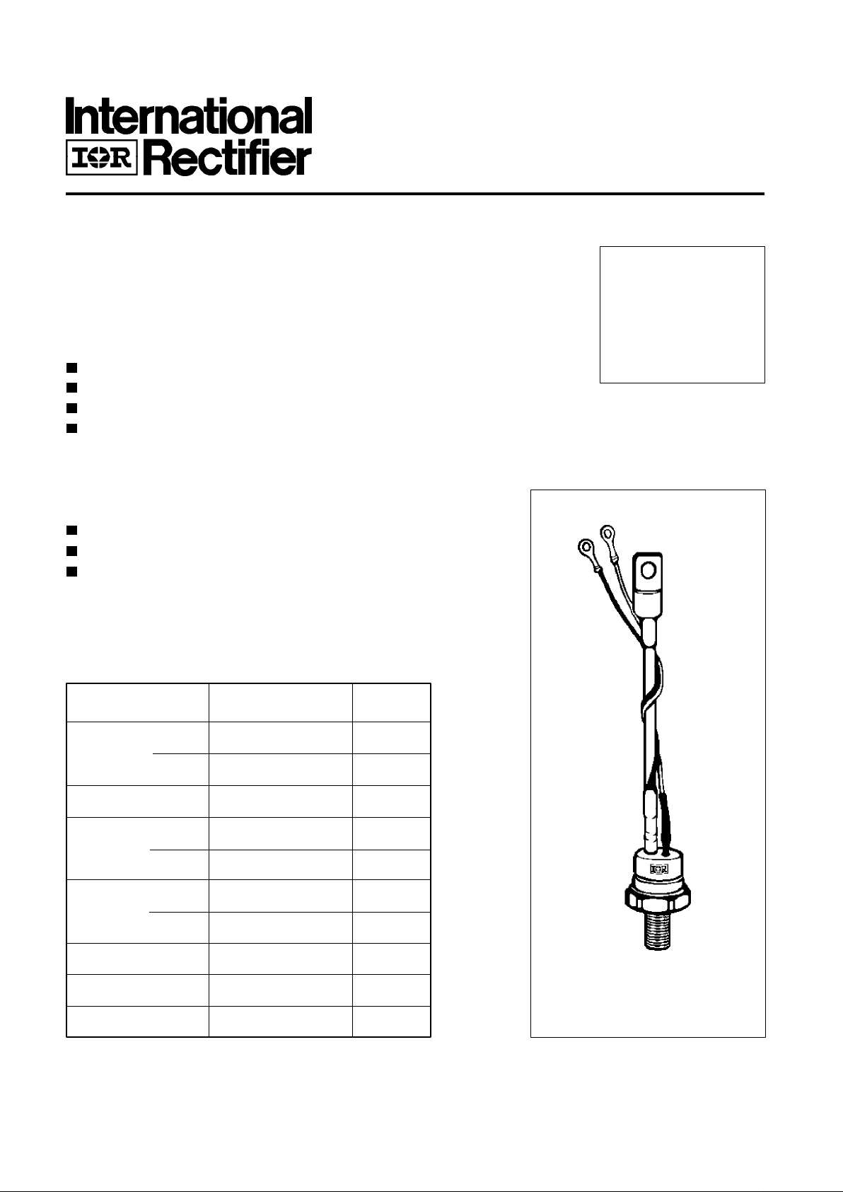
International standard case TO-209AC (TO-94)
Threaded studs UNF 1/2 - 20UNF2A or ISO M12x1.75
Major Ratings and Characteristics
case style
TO-209AC (TO-94)
Page 2
80RIA Series
2222222222222
12
I
T(AV)
Max. average on-state current 80 A 180° conduction, half sine wave
@ Case temperature 85 °C
I
T(RMS)
Max. RMS on-state current 125 A DC @ 75°C case temperature
I
TSM
Max. peak, one-cycle 1900 t = 10ms No voltage
non-repetitive surge current 1990 t = 8.3ms reapplied
1600 t = 10ms 100% V
RRM
1675 t = 8.3ms reapplied Sinusoidal half wave,
I
2
t Maximum I2t for fusing 18 t = 10ms No voltage Initial TJ = TJ max.
16 t = 8.3ms reapplied
12.7 t = 10ms 100% V
RRM
11.7 t = 8.3ms reapplied
I
2
√t Maximum I2√t for fusing 180.5 KA2√s t = 0.1 to 10ms, no voltage reapplied
V
T(TO)1
Low level value of threshold
voltage
V
T(TO)
2
High level value of threshold
voltage
r
t1
Low level value of on-state
slope resistance
r
t2
High level value of on-state
slope resistance
V
TM
Max. on-state voltage 1.60 V Ipk= 250A, TJ = 25°C tp = 10ms sine pulse
I
H
Maximum holding current 150
I
L
Typical latching current 400
0.99 (16.7% x π x I
T(AV)
< I < π x I
T(AV)
), TJ = TJ max.
2.29 (16.7% x π x I
T(AV)
< I < π x I
T(AV)
), TJ = TJ max.
1.84 (I > π x I
T(AV)
),TJ = TJ max.
Parameter 80RIA Units Conditions
1.13 (I > π x I
T(AV)
),TJ = TJ max.
On-state Conduction
KA2s
mΩ
V
A
mA
T
J
= 25°C, anode supply 12V resistive load
ELECTRICAL SPECIFICATIONS
Voltage Ratings
Voltage V
DRM/VRRM
, max. repetitive V
RSM
, maximum non- I
DRM/IRRM
max.
Type number Code peak and off-state voltage repetitive peak voltage
@ TJ = 125°C
V V mA
40 400 500
80RIA 80 800 900 15
120 1200 1300
Page 3
80RIA Series
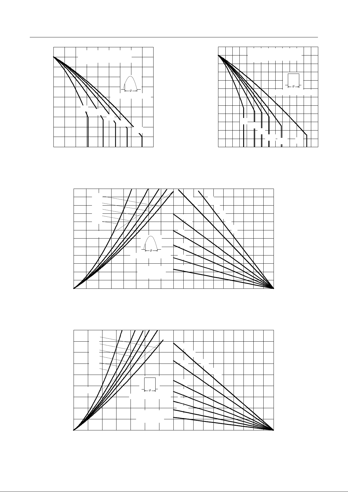
Fig. 1 - Current Ratings Characteristics Fig. 2 - Current Ratings Characteristics
Fig. 3 - On-state Power Loss Characteristics
Fig. 4 - On-state Power Loss Characteristics
Page 4

80RIA Series
Fig. 5 - Maximum Non-Repetitive Surge Current Fig. 6 - Maximum Non-Repetitive Surge Current
Fig. 7 - On-state Voltage Drop Characteristics
Fig. 8 - Thermal Impedance Z
thJC
Characteristics
Page 5

80RIA Series
Fig. 9 - Gate Characteristics
Page 6

80RIA Series
23
di/dt Max. non-repetitive rate of rise TJ = 125°C, Vd = rated V
DRM
, I
TM
= 2xdi/dt snubber
of turned-on current 300 A/µs 0.2µF, 15Ω, Gate pulse: 20V, 65Ω, t
p
= 6µs, tr= 0.5µs
Per JEDEC Standard RS-397, 5.2.2.6.
Gate pulse: 10V, 15Ω source, t
p
= 6µs, tr = 0.1µs,
V
d
= rated V
DRM
, I
TM
= 50Adc, TJ = 25°C.
I
TM
= 50A, TJ = TJ max, di/dt = -5A/µs min., VR = 50V,
dv/dt
= 20V/µs, Gate bias: 0V 25Ω, tp = 500µs
dv/dt Maximum critical rate of rise of
off-state voltage
I
RRM
Max. peak reverse and off-state
I
DRM
leakage current
Blocking
Parameter 80RIA Units Conditions
15 mA TJ = 125°C rated V
DRM/VRRM
applied
P
GM
Maximum peak gate power 12 TJ = TJ max, tp ≤ 5ms
P
G(AV)
Maximum average gate power 3 TJ = TJ max, f = 50Hz, d% = 50
I
GM
Max. peak positive gate current 3 A TJ = TJ max, tp ≤ 5ms
+V
GM
Maximum peak positive
gate voltage
-V
GM
Maximum peak negative
gate voltage
I
GT
Max. DC gate current required 270 TJ = - 40°C
to trigger 120 mA T
J
= 25°C
60 T
J
= 125°C
V
GT
Max. DC gate voltage required 3.5 TJ = - 40°C
to trigger 2.5 V T
J
= 25°C
1.5 T
J
= 125°C
I
GD
DC gate current not to trigger 6 mA
Parameter 80RIA Units Conditions
Triggering
W
20
10
V T
J
= TJ max, tp ≤ 5ms
V
GD
DC gate voltage not to trigger 0.25 V
Max. gate current/ voltage not to
trigger is the max. value which
will not trigger any unit with rated
V
DRM
anode-to-cathode applied
T
J
= TJ max
Max. required gate trigger/ current/ voltage are the lowest value
which will trigger all units 6V anode-to-cathode applied
Parameter 80RIA Units Conditions
Switching
µs
500 V/µs TJ = 125°C exponential to 67% rated V
DRM
t
d
Typical delay time 1
t
q
Typical turn-off time 110
Page 7

80RIA Series
2222222222222
12
180° 0.042 0.030 TJ = TJ max.
120° 0.050 0.052
90° 0.064 0.070 K/W
60° 0.095 0.100
30° 0.164 0.165
Ordering Information Table
1 - I
TAV
x 10A
2 - 0 = Eyelet terminals (Gate and Auxiliary Cathode Leads)
1 = Fast - on terminals (Gate and Auxiliary Cathode Leads)
2 = Flag terminals (For Cathode and Gate Terminals)
3 - RIA = Essential part number
4 - Voltage code: Code x 10 = V
RRM
(See Voltage Rating Table)
5 - None = Stud base 1/2 "20UNF - 2A threads
M = Stud base metric threads M12 x 1.75 E 6
4
8 0 RIA 120 M
Device Code
1 2
T
J
Max. operating temperature range -40 to 125
T
stg
Max. storage temperature range -40 to 150
R
thJC
Max. thermal resistance,
junction to case
R
thCS
Max. thermal resistance,
case to heatsink
T Mounting torque, ± 10% 15.5 (137) Non lubricated threads
14 (120) Lubricated threads
wt Approximate weight 130 g
Parameter 80RIA Units Conditions
0.30 DC operation
0.1 Mounting surface, smooth, flat and greased
Thermal and Mechanical Specification
°C
K/W
Nm
(lbf-in)
3
5
Case style TO-209AC(TO-94) See Outline Table
Conduction angle Sinusoidal conduction Rectangular conduction Units Conditions
∆R
thJ-C
Conduction
(The following table shows the increment of thermal resistence R
thJ-C
when devices operate at different conduction angles than DC)
Page 8

80RIA Series
23
Outline Table
Fast-on Terminals
Case Style TO-209AC (TO-94)
All dimensions in millimeters (inches)
WHITE SHRINK
C.S. 0.4 mm
2
215 (8.46)
10 (0.39)
WHITE GATE
RED SHRINK
RED CATHODE
RED SILICON RUBBER
4.3 (0.17) DIA.
21 (0.83)
* FOR METRIC DEVICE : M12 x 1.75 E 6
10 (0.39) MA X.
157 (6.18)
170 (6.6 9)
(.0006 s.i.)
GLASS METAL SEAL
8.5 (0.3) DIA.
16.5 (0.65) MAX.
23.5 (0.92) MAX. DIA.
MAX .
24 (0.94) MA X.
55 (2.17) M IN.
C.S. 16mm
2
FLEXIBLE LEAD
(.025 s.i.)
2.5 (0.10) MAX.
2
0
(
0
.
7
9
)
M
I
N
.
1/2"-20UNF-2A *
SW 27
29.5 (1.16) MAX.
9
.
5
(
0
.
3
7
)
M
I
N
.
Case Style TO-208AD (TO-83)
All dimensions in millimeters (inches)
12
1/2"-20UNF-2A *
29.5 (1.16)
* FOR METRIC DEVICE: M12 x 1.75 E 6
M AX.
44 (1.7 3)
10
23.5 DIA.
16 .5
(0 .6 5)
10 (0 .39 )
24 (0.9 4) M AX .
(0 39 )
(0.93) MAX.
21( 0.83 )
1.5 (0.06) DIA.
(0 .4 7)
47 (1 .85 )
M A X .
GLASS-METAL SEAL
FLAG TERMINALS
SW 27
2.4 (0.09)
5.6 (0.22)
5.5 (0.22) DIA.
AMP. 280000-1
REF-250
 Loading...