

Page 1
82C84A
March 1997
Features
• Generates the System Clock For CMOS or NMOS
Microprocessors
• Up to 25MHz Operation
• Uses a Parallel Mode Crystal Circuit or External
Frequency Source
• Provides Ready Synchronization
• Generates System Reset Output From Schmitt Trigger
Input
• TTL Compatible Inputs/Outputs
• Very Low Power Consumption
• Single 5V Power Supply
• Operating Temperature Ranges
- C82C84A . . . . . . . . . . . . . . . . . . . . . . . . .0
- I82C84A. . . . . . . . . . . . . . . . . . . . . . . . -40
- M82C84A. . . . . . . . . . . . . . . . . . . . . . -55
o
C to +70oC
o
C to +85oC
o
C to +125oC
CMOS Clock Generator Driver
Description
The Intersil 82C84A is a high performance CMOS Clock Generatordriver which is designed to service the requirements of both CMOS
and NMOS microprocessors such as the 80C86, 80C88, 8086 and
the 8088. The chip contains a crystal controlled oscillator, a divide-bythree counter and complete “Ready” synchronization and reset logic.
Static CMOS circuit design permits operation with an external frequency source from DC to 25MHz. Crystal controlled operation to
25MHz is guaranteed with the use of a parallel, fundamental mode
crystal and two small load capacitors.
All inputs (except X1 and RES) are TTL compatible over temperature and voltage ranges.
Power consumption is a fraction of that of the equivalent bipolar circuits. This speed-power characteristic of CMOS permits the
designer to custom tailor his system design with respect to power
and/or speed requirements.
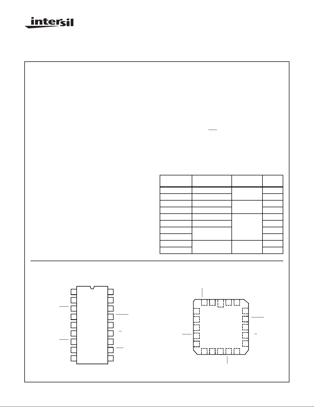
Ordering Information
PART
NUMBER TEMP. RANGE PACKAGE
CP82C84A 0oC to +70oC 18 Ld PDIP E18.3
IP82C84A -40oC to +85oC E18.3
CS82C84A 0oC to +70oC 20 Ld PLCC N20.35
IS82C84A -40oC to +85oC N20.35
CD82C84A 0oC to +70oC 18 Ld CERDIP F18.3
ID82C84A -40oC to +85oC F18.3
MD82C84A/B -55oC to +125oC F18.3
8406801VA SMD# F18.3
MR82C84A/B -55oC to +125oC 20 Pad CLCC J20.A
84068012A SMD# J20.A
PKG.
NO.
Pinouts
82C84A (PDIP, CERDIP)
TOP VIEW
PCLK
AEN1
RDY1
RDY2
AEN2
CLK
GND
1
2
3
4
5
6
7
8
9
| Copyright © Intersil Corporation 1999
CSYNC
READY
CAUTION: These devices are sensitive to electrostatic discharge; follow proper IC Handling Procedures.
http://www.intersil.com or 407-727-9207
18
17
16
15
14
13
12
11
10
V
CC
X1
X2
ASYNC
EFI
C
F/
OSC
RES
RESET
RDY1
READY
RDY2
AEN2
4-287
82C84A (PLCC, CLCC)
TOP VIEW
AEN1
3212019
4
5
6
7
8
NC
9101112
CLK
PCLK
GND
CSYNC
V
RESET
CC
X1
18
X2
17
ASYNC
EFI
16
15
C
F/
14
NC
13
RES
OSC
File Number 2974.1
Page 2
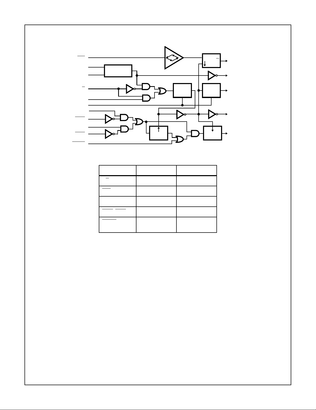
Functional Diagram
82C84A
RES
X1
X2
F/
EF1
CSYNC
RDY1
AEN1
RDY2
AEN2
ASYNC
11
17
16
13
C
14
1
4
3
6
7
15
XTAL
OSCILLATOR
CK
DQ
FF1
÷ 3
SYNC
D
CK
SYNC
CK
DQ
÷ 2
FF2
10
Q
RESET
12
OSC
2
PCLK
8
CLK
5
READY
CONTROL PIN LOGICAL 1 LOGICAL 0
F/C External Clock Crystal Drive
RES Normal Reset
RDY1, RDY2 Bus Ready Bus Not Ready
AEN1, AEN2 Address Disabled Address Enable
ASYNC 1 Stage Ready
Synchronization
2 Stage Ready
Synchronization
4-288
Page 3
82C84A
Pin Description
SYMBOL NUMBER TYPE DESCRIPTION
AEN1,
AEN2
RDY1,
RDY2
ASYNC 15 I READY SYNCHRONIZATION SELECT: ASYNC is an input which defines the synchronization
READY 5 O READY: READY is an active HIGH signal which is the synchronized RDY signal input. READY
X1, X2 17, 16 I O CRYSTAL IN: X1 and X2 are the pins to which a crystal is attached. The crystal frequency is 3
F/C 13 I FREQUENCY/CRYSTAL SELECT: F/C is a strapping option. When strapped LOW. F/C permits
EFI 14 I EXTERNAL FREQUENCY IN: When F/C is strapped HIGH, CLK is generated from the input fre-
CLK 8 O PROCESSOR CLOCK: CLK is the clock output used by the processor and all devices which di-
3, 7 I ADDRESS ENABLE: AEN is an active LOW signal. AEN serves to qualify its respective Bus
Ready Signal (RDY1 or RDY2). AEN1 validates RDY1 while AEN2 validates RDY2. Two AEN
signal inputs are useful in system configurations which permit the processor to access two MultiMaster System Busses. In non-Multi-Master configurations, the AEN signal inputs are tied true
(LOW).
4, 6 I BUS READY (Transfer Complete). RDY is an active HIGH signal which is an indication from a
device located on the system data bus that data has been received, or is available RDY1 is qualified by AEN1 while RDY2 is qualified by AEN2.
mode of the READY logic. When ASYNC is low, two stages of READY synchronization are provided. When ASYNC is left open or HIGH, a single stage of READY synchronization is provided.
is cleared after the guaranteed hold time to the processor has been met.
times the desired processor clock frequency, (Note 1).
the processor’s clock to be generated by the crystal. When F/C is strapped HIGH, CLK is generated for the EFI input, (Note 1).
quency appearing on this pin. The input signal is a square wave 3 times the frequency of the desired CLK output.
rectly connect to the processor’s local bus. CLK has an output frequency which is 1/3 of the crystal or EFI input frequency and a 1/3 duty cycle.
PCLK 2 O PERIPHERAL CLOCK: PCLK is a peripheral clock signal whose output frequency is 1/2 that of
CLK and has a 50% duty cycle.
OSC 12 O OSCILLATOR OUTPUT: OSC is the output of the internal oscillator circuitry. Its frequency is
equal to that of the crystal.
RES 11 I RESET IN: RES is an active LOW signal which is used to generate RESET. The 82C84A pro-
vides a Schmitt trigger input so that an RC connection can be used to establish the power-up
reset of proper duration.
RESET 10 O RESET: RESET is an active HIGH signal which is used to reset the 80C86 family processors. Its
timing characteristics are determined by RES.
CSYNC 1 I CLOCK SYNCHRONIZATION: CSYNC is an active HIGH signal which allows multiple 82C84As
to be synchronized to provide clocks that are in phase. When CSYNC is HIGH the internal
counters are reset. When CSYNC goes LOW the internal counters are allowed to resume counting. CSYNC needs to be externally synchronized to EFI. When using the internal oscillator
CSYNC should be hardwired to ground.
GND 9 Ground
V
CC
NOTE:
1. If the crystal inputs are not used X1 must be tied to VCC or GND and X2 should be left open.
18 VCC: The +5V power supply pin. A 0.1µF capacitor between VCC and GND is recommended for
decoupling.
4-289
Page 4

82C84A
Functional Description
Oscillator
The oscillator circuit of the 82C84A is designed primarily for
use with an external parallel resonant, fundamental mode
crystal from which the basic operating frequency is derived.
The crystal frequency should be selected at three times the
required CPU clock. X1 and X2 are the two crystal input
crystal connections. For the most stable operation of the
oscillator (OSC) output circuit, two capacitors (C1 = C2) as
shown in the waveform figures are recommended. The output of the oscillator is buffered and brought out on OSC so
that other system timing signals can be derived from this stable, crystal-controlled source.
TABLE 1. CRYSTAL SPECIFICATIONS
PARAMETER TYPICAL CRYSTAL SPEC
Frequency 2.4 - 25MHz, Fundamental, “AT” cut
Type of Operation Parallel
Unwanted Modes 6dB (Minimum)
Load Capacitance 18 - 32pF
Capacitors C1, C2 are chosen such that their combined
capacitance
C1 x C2
--------------------- -
CT =
C1 + C2
matches the load capacitance as specified by the crystal
manufacturer. This ensures operation within the frequency
tolerance specified by the crystal manufacturer.
Clock Generator
The clock generator consists of a synchronous divide-bythree counter with a special clear input that inhibits the
counting. This clear input (CSYNC) allows the output clock
to be synchronized with an external event (such as another
82C84A clock). It is necessary to synchronize the CSYNC
input to the EFI clock external to the 82C84A. This is accomplished with two flip-flops. (See Figure 1). The counter output is a 33% duty cycle clock at one-third the input
frequency.
NOTE: The F/C input is a strapping pin that selects either the crystal
oscillator or the EFI input as the clock for the ÷ 3 counter. If
the EFI input is selected as the clock source, the oscillator
section can be used independently for another clock source.
Output is taken from OSC.
(Including stray capacitance)
Clock Outputs
The CLK output is a 33% duty cycle clock driver designed to
drive the 80C86, 80C88 processors directly. PCLK is a peripheral clock signal whose output frequency is 1/2 that of CLK.
PCLK has a 50% duty cycle.
Reset Logic
The reset logic provides a Schmitt trigger input (RES) and a
synchronizing flip-flop to generate the reset timing. The reset
signal is synchronized to the falling edge of CLK. A simple RC
network can be used to provide power-on reset by utilizing this
function of the 82C84A.
READY Synchronization
Two READY input (RDY1, RDY2) are provided to accommodate two system busses. Each input has a qualifier (
AEN1 and
AEN2, respectively). The AEN signals validate their respective
RDY signals. If a Multi-Master system is not being used the
AEN pin should be tied LOW.
Synchronization is required for all asynchronous active-going
edges of either RDY input to guarantee that the RDY setup
and hold times are met. Inactive-going edges of RDY in normally ready systems do not require synchronization but must
satisfy RDY setup and hold as a matter of proper system
design.
ASYNC input defines two modes of READY synchroniza-
The
tion operation.
When ASYNC is LOW, two stages of synchronization are provided for active READY input signals. Positive-going asynchronous READY inputs will first be synchronized to flip-flop one of
the rising edge of CLK (requiring a setup time tR1VCH) and
the synchronized to flip-flop two at the next falling edge of
CLK, after which time the READY output will go active (HIGH).
Negative-going asynchronous READY inputs will be synchronized directly to flip-flop two at the falling edge of CLK, after
which the READY output will go inactive. This mode of operation is intended for use by asynchronous (normally not ready)
devices in the system which cannot be guaranteed by design
to meet the required RDY setup timing, TR1VCL, on each bus
cycle.
ASYNC is high or left open, the first READY flip-flop is
When
bypassed in the READY synchronization logic. READY inputs
are synchronized by flip-flop two on the falling edge of CLK
before they are presented to the processor. This mode is available for synchronous devices that can be guaranteed to meet
the required RDY setup time.
ASYNC can be changed on every bus cycle to select the
appropriate mode of synchronization for each device in the
system.
EFI
CLOCK
SYNCHRONIZE
EFI
NOTE: If EFI input is used, then crystal input X1 must be tied to VCC or GND and X2 should be left open. If the crystal inputs are used,
then EFI should be tied to VCC or GND.
FIGURE 1. CSYNC SYNCHRONIZATION
DQ>D
Q
>
82C84A
CSYNC
(TO OTHER 82C84As)
4-290
Page 5

82C84A
Absolute Maximum Ratings Thermal Information
Supply Voltage . . . . . . . . . . . . . . . . . . . . . . . . . . . . . . . . . . . . .+8.0V
Input, Output or I/O Voltage . . . . . . . . . . . GND -0.5V to VCC+0.5V
ESD Classification . . . . . . . . . . . . . . . . . . . . . . . . . . . . . . . . Class 1
Operating Conditions
Operating Voltage Range . . . . . . . . . . . . . . . . . . . . . +4.5V to +5.5V
Operating Temperature Range
C82C84A . . . . . . . . . . . . . . . . . . . . . . . . . . . . . . . . 0oC to +70oC
I82C84A . . . . . . . . . . . . . . . . . . . . . . . . . . . . . . . . -40oC to +85oC
M82C84A . . . . . . . . . . . . . . . . . . . . . . . . . . . . . . -55oC to +125oC
CAUTION: Stresses above those listed in “Absolute Maximum Ratings” may cause permanent damage to the device. This is a stress only rating and operation
of the device at these or any other conditions above those indicated in the operational sections of this specification is not implied.
Thermal Resistance . . . . . . . . . . . . . . . . θJA(oC/W) θJC (oC/W)
CERDIP Package . . . . . . . . . . . . . . . . 80 20
CLCC Package . . . . . . . . . . . . . . . . . . 95 28
PDIP Package. . . . . . . . . . . . . . . . . . . 85 N/A
PLCC Package . . . . . . . . . . . . . . . . . . 85 N/A
Storage Temperature Range. . . . . . . . . . . . . . . . . .-65oC to +150oC
Max Junction Temperature . . . . . . . . . . . . . . . . . . . . . . . . . .+175oC
Lead Temperature (Soldering 10s) . . . . . . . . . . . . . . . . . . . . +300oC
(PLCC - Lead Tips Only)
Die Characteristics
Gate Count . . . . . . . . . . . . . . . . . . . . . . . . . . . . . . . . . . . . .50 Gates
DC Electrical Specifications V
SYMBOL PARAMETER MIN MAX UNITS TEST CONDITIONS
V
V
V
V
VT+ - VT- Reset Input Hysteresis 0.2 V
V
V
I
CCOP
NOTES:
1. F/C is a strap option and should be held either ≤ 0.8V or ≥ 2.2V. Does not apply to X1 or X2 pins.
2. Due to test equipment limitations related to noise, the actual tested value may differ from that specified, but the specified limit is
guaranteed.
3. CSYNC pin is tested with VIL≤ 0.8V.
4. ASYNC pin includes an internal 17.5kΩ nominal pull-up resistor. For ASYNC input at GND, ASYNC input leakage current = 300µA
nominal, X1 - crystal feedback input.
5. f = 25MHz may be tested using the extrapolated value based on measurements taken at f = 2MHz and f = 10MHz.
Logical One Input Voltage 2.0
IH
Logical Zero Input Voltage - 0.8 V Notes 1, 2, 3
IL
Reset Input High Voltage VCC -0.8 - V
IHR
Reset Input Low Voltage - 0.5 V
ILR
Logical One Output Current VCC -0.4 - V IOH = -4.0mA for CLK Output
OH
Logical Zero Output Voltage - 0.4 V IOL = +4.0mA for CLK Output
OL
II Input Leakage Current -1.0 1.0 µAVIN = VCC or GND except ASYNC,
Operating Power Supply Current - 40 mA Crystal Frequency = 25MHz
= +5.0V ±10%,
CC
TA = 0oC to +70oC (C82C84A),
TA = -40oC to +85oC (I82C84A),
TA = -55oC to +125oC (M82C84A)
2.2
CC
-V
V
--
C82C84A, I82C84
M82C84A, Notes 1, 2
IOH = -2.5mA for All Others
IOL = +2.5mA for All Others
X1: (Note 4)
Outputs Open, Note 5
Capacitance T
SYMBOL PARAMETER TYPICAL UNITS TEST CONDITIONS
C
IN
C
OUT
= +25oC
A
Input Capacitance 10 pF FREQ = 1MHz, all measurements are
Output Capacitance 15 pF
referenced to device GND
4-291
Page 6

82C84A
AC Electrical Specifications V
SYMBOL PARAMETER
TIMING REQUIREMENTS
(1) TEHEL External Frequency HIGH Time 13 - ns 90%-90% V
(2) TELEH External Frequency LOW Time 13 - ns 10%-10% V
(3) TELEL EFI Period 36 - ns
XTAL Frequency 2.4 25 MHz Note 2
(4) TR2VCL RDY1, RDY2 Active Setup to CLK 35 - ns ASYNC = HIGH
(5) TR1VCH RDY1, RDY2 Active Setup to CLK 35 - ns ASYNC = LOW
(6) TR1VCL RDY1, RDY2 Inactive Setup to CLK 35 - ns
(7) TCLR1X RDY1, RDY2 Hold to CLK 0 - ns
(8) TAYVCL
(9) TCLAYX
(10) TA1VR1V
(11) TCLA1X
(12) TYHEH CSYNC Setup to EFI 20 - ns
(13) TEHYL CSYNC Hold to EFI 20 - ns
(14) TYHYL CSYNC Width 2TELEL - ns
(15) TI1HCL
(16) TCLI1H
TIMING RESPONSES
(17) TCLCL CLK Cycle Period 125 - ns Note 6
(18) TCHCL CLK HIGH Time (1/3 TCLCL) +2.0 - ns Note 6
(19) TCLCH CLK LOW Time (2/3 TCLCL) -15.0 - ns Note 6
(20)
TCH1CH2
(21)
TCL2CL1
(22) TPHPL PCLK HIGH Time TCLCL-20 - ns Note 6
(23) TPLPH PCLK LOW Time TCLCL-20 - ns Note 6
(24) TRYLCL Ready Inactive to CLK (See Note 4) -8 - ns Note 4
(25) TRYHCH Ready Active to CLK (See Note 3) (2/3 TCLCL) -15.0 - ns Note 5
(26) TCLIL CLK to Reset Delay - 40 ns
(27) TCLPH CLK to PCLK HIGH Delay - 22 ns
(28) TCLPL CLK to PCLK LOW Delay - 22 ns
(29) TOLCH OSC to CLK HIGH Delay -5 22 ns
(30) TOLCL OSC to CLK LOW Delay 2 35 ns
NOTES:
1. Tested as follows: f = 2.4MHz, V
switch between 0.4V and VCC -0.4V. Input rise and fall times driven at 1ns/V. VIL≤ VIL (max) - 0.4V for CSYNC pin. VCC = 4.5V and 5.5V.
2. Tested using EFI or X1 input pin.
3. Setup and hold necessary only to guarantee recognition at next clock.
4. Applies only to T2 states.
5. Applies only to T3 TW states.
6. Tested with EFI input frequency = 4.2MHz.
ASYNC Setup to CLK 50 - ns
ASYNC Hold to CLK 0 - ns
AEN1, AEN2 Setup to RDY1, RDY2 15 - ns
AEN1, AEN2 Hold to CLK 0 - ns
RES Setup to CLK 65 - ns Note 3
RES Hold to CLK 20 - ns Note 3
CLK Rise or Fall Time - 10 ns 1.0V to 3.0V
IH
= +5V± 10%,
CC
TA = 0oC to +70oC (C82C84A),
TA = -40oC to +85oC (I82C84A),
TA = -55oC to +125oC (M82C84A)
LIMITS
UNITS
= 2.6V, VIL = 0.4V, CL = 50pF, VOH≥ 1.5V, VOL≤ 1.5V, unless otherwise specified. RES and F/C must
(NOTE 1)
TEST
CONDITIONSMIN MAX
IN
IN
4-292
Page 7

Timing Waveforms
82C84A
(3)
NAME
EFI
OSC
CLK
PCLK
CSYNC
RES
RESET
I/O
I
O
O
O
I
I
O
(13)
tEHYL
tYHYL
(14)
tELEL
tOLCH
(29)
tCH1CH2
(20)
tYHEH
(12)
tCL2CL1
(21)
(30)
tOLCL
NOTE: All timing measurements are made at 1.5V, unless otherwise noted.
FIGURE 2. WAVEFORMS FOR CLOCKS AND RESETS SIGNALS
CLK
tR1VCH
(10)
(5)
(7)
tCLAYX
tAYVCL
(8)
(9)
(25)
tRYHCH
tCLR1X
RDY1, 2
tA1VR1V
AEN1, 2
ASYNC
READY
tCLA1X
tCLPH
(27)
tPLPH
(23)
tR1VCL
(7)tCLR1X
(11)
(24) tRYLCL
tELEH
tCLI1H
(6)
(19)
tCLCH
(17) tCLCL
tPHPL
(16)
(2)
(22)
tCLIL
(15)
tI1HCL
(26)
(1)
tEHEL
tCHCL
(18)
tCLPL
(28)
FIGURE 3. WAVEFORMS FOR READY SIGNALS (FOR ASYNCHRONOUS DEVICES)
CLK
tCLR1X
RDY 1, 2
tA1VRIV
AEN1, 2
(8)
ASYNC
READY
(10)
tA YVCL
tCLAYX
(7)
(4)
tR1VCL
(9)
(25)
tRYHCH
tCLR1X
tCLA1X
(7)
(11)
(24)
tRYLCL
FIGURE 4. WAVEFORMS FOR READY SIGNALS (FOR SYNCHRONOUS DEVICES)
4-293
tR1VCL
(6)
Page 8

Test Load Circuits
DEVICE UNDER TEST
NOTES:
1. CL =100pF for CLK output.
2. CL = 50pF for all outputs except CLK.
3. CL = Includes probe and jig capacitance.
82C84A
2.25V
R = 740Ω FOR ALL OUTPUTS
EXCEPT CLK
OUTPUT FROM
FIGURE 5. TEST LOAD MEASUREMENT CONDITIONS
463Ω FOR CLK OUTPUT
C
L
(SEE NOTE 3)
C1
24MHz
PULSE
GENERATOR
TRIGGER
C2
C1
C2
X1
X2
C
F/
CSYNC
CLK
LOAD
(SEE NOTE 1)
PULSE
GENERATOR
EF1
V
CC
F/
CSYNC
CLK
C
LOAD
(SEE NOTE 1)
FIGURE 6. TCHCL, TCLCH LOAD CIRCUITS
V
CC
AEN1
X1
X2
RDY2
F/
C
AEN2
CSYNC
CLK
READY
OSC
LOAD
(SEE NOTE 1)
LOAD
(SEE NOTE 2)
PULSE
GENERATOR
TRIGGER
PULSE
GENERATOR
EF1
V
CC
F/
AEN1
RDY2
AEN2
CSYNC
CLK
C
READY
LOAD
(SEE NOTE 1)
LOAD
(SEE NOTE 2)
FIGURE 7. TRYLCL, TRYHCH LOAD CIRCUITS
AC Testing Input, Output Waveform
INPUT
+ 0.4V
V
IH
1.5V 1.5V
VIL - 0.4V
NOTE: Input test signals must s witch between VIL (maximum) -0.4V and VIH (minimum) +0.4V. RES and F/C must switch between 0.4V and
VCC -0.4V. Input rise and fall times driven at 1ns/V. VIL≤ VIL (max) -0.4V for CSYNC pin. VCC -4.5V and 5.5V.
4-294
OUTPUT
V
OH
V
OL
Page 9

Burn-In Circuits
V
CC
GND
V
CC
GND
V
CC
GND
F9
F6
F5
F7
F8
R2
R2
R2
R2
R2
R2
R1
R1
R1
R1
R1
82C84A
MD82C84A CERDIP
1
2
3
4
5
6
7
8
9
MR82C84A CLCC
V
CC
C1
18
17
16
R3
15
R1
14
R1
13
12
R1
11
10
R1
R2
R2
R2
R2
R2
F0
OPEN
F10
F1
F11
V
CC
GND
F12
V
CC
GND
V
NOTES:
= 5.5V ±0.5V, GND = 0V.
V
CC
VIH = 4.5V ±10%.
VIL = -0.2 to 0.4V.
R1 = 47kΩ,±5%.
R2 = 10kΩ,±5%.
R3 = 2.2kΩ,±5%.
R4 = 1.2kΩ,±5%.
C1 = 0.01µF (minimum).
F0 = 100kHz ±10%.
F1 = F0/2, F2 = F1/2, . . . F12 = F11/2.
F5
/ 2
CC
F7
F8
OPEN
R4
R4
R4
R4
/ 2
CC
F6
F9
V
R4
R4R4R4
3212019
4
5
6
7
8
9101112
R4
R4R4R4
/ 2
/ 2
CC
CC
V
V
V
CC
C1
F0
F12
18
17
16
15
14
13
/ 2
CC
V
R4
R4
R4
OPEN
F10
F1
F11
OPEN
4-295
Page 10

Die Characteristics
82C84A
DIE DIMENSIONS:
66.1 x 70.5 x 19 ± 1mils
METALLIZATION:
Type: Si - AI
Thickness: 11k
Å ± 1kÅ
Metallization Mask Layout
AEN1 PCLK CSYNC V
RDY1
READY
RDY2
GLASSIVATION:
Type: SiO
2
Thickness: 8kű 1kÅ
WORST CASE CURRENT DENSITY:
1.42 x 10
82C84A
CC
5
A/cm
2
X1
X2
ASYNC
EFI
AEN2
CLK
GND RESET
RES OSC
F/
C
All Intersil semiconductor products are manufactured, assembled and tested under ISO9000 quality systems certification.
Intersil products are sold by description only. Intersil Corporation reserves the right to make changes in circuit design and/or specifications at any time without
notice. Accordingly, the reader is cautioned to verify that data sheets are current before placing orders. Information furnished by Intersil is believed to be accurate
and reliable. However, no responsibility is assumed by Intersil or its subsidiaries for its use; nor for any infringements of patents or other rights of third parties which
may result from its use. No license is granted by implication or otherwise under an y patent or patent rights of Intersil or its subsidiaries.
For information regarding Intersil Corporation and its products, see web site http://www.intersil.com
Sales Office Headquarters
NORTH AMERICA
Intersil Corporation
P. O. Box 883, Mail Stop 53-204
Melbourne, FL 32902
TEL: (407) 724-7000
FAX: (407) 724-7240
EUROPE
Intersil SA
Mercure Center
100, Rue de la Fusee
1130 Brussels, Belgium
TEL: (32) 2.724.2111
FAX: (32) 2.724.22.05
ASIA
Intersil (Taiwan) Ltd.
Taiwan Limited
7F-6, No. 101 Fu Hsing North Road
Taipei, Taiwan
Republic of China
TEL: (886) 2 2716 9310
FAX: (886) 2 2715 3029
4-296
 Loading...