

Page 1
82C55A
CHMOS PROGRAMMABLE PERIPHERAL INTERFACE
Y
Compatible with all Intel and Most
Other Microprocessors
Y
High Speed, ‘‘Zero Wait State’’
Operation with 8 MHz 8086/88 and
80186/188
Y
24 Programmable I/O Pins
Y
Low Power CHMOS
Y
Completely TTL Compatible
Y
Control Word Read-Back Capability
Y
Direct Bit Set/Reset Capability
Y
2.5 mA DC Drive Capability on all I/O
Port Outputs
Y
Available in 40-Pin DIP and 44-Pin PLCC
Y
Available in EXPRESS
Ð Standard Temperature Range
Ð Extended Temperature Range
The Intel 82C55A is a high-performance, CHMOS version of the industry standard 8255A general purpose
programmable I/O device which is designed for use with all Intel and most other microprocessors. It provides
24 I/O pins which may be individually programmed in 2 groups of 12 and used in 3 major modes of operation.
The 82C55A is pin compatible with the NMOS 8255A and 8255A-5.
In MODE 0, each group of 12 I/O pins may be programmed in sets of 4 and 8 to be inputs or outputs. In
MODE 1, each group may be programmed to have 8 lines of input or output. 3 of the remaining 4 pins are used
for handshaking and interrupt control signals. MODE 2 is a strobed bi-directional bus configuration.
The 82C55A is fabricated on Intel’s advanced CHMOS III technology which provides low power consumption
with performance equal to or greater than the equivalent NMOS product. The 82C55A is available in 40-pin
DIP and 44-pin plastic leaded chip carrier (PLCC) packages.
231256– 31
231256– 1
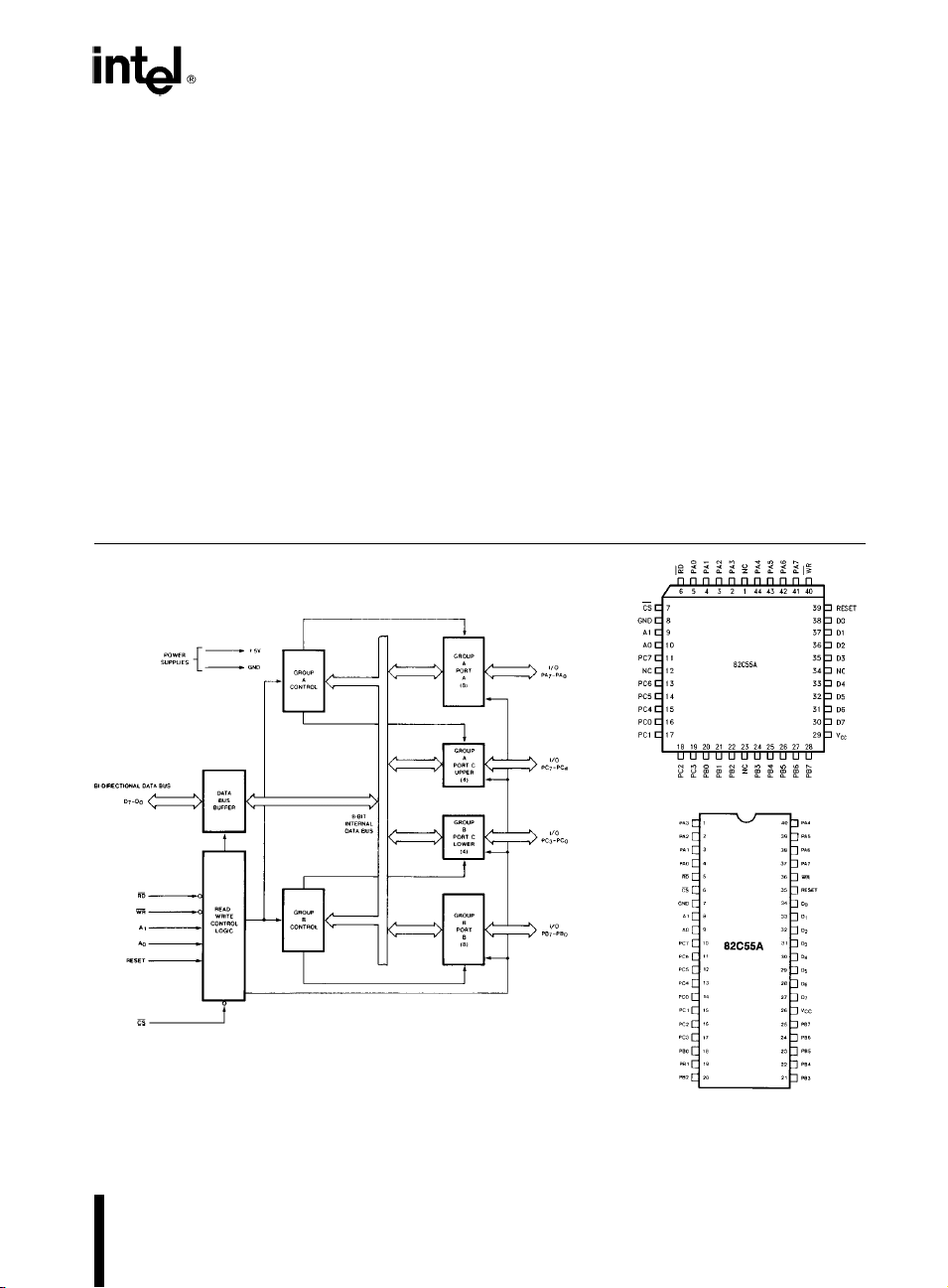
Figure 1. 82C55A Block Diagram
Figure 2. 82C55A Pinout
Diagrams are for pin reference only. Package
sizes are not to scale.
October 1995 Order Number: 231256-004
231256– 2
Page 2
82C55A
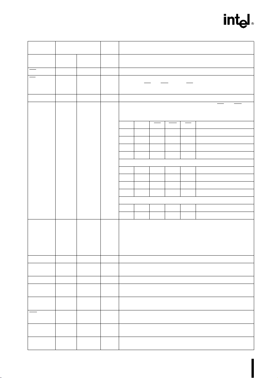
Table 1. Pin Description
Symbol
PA
3–0
RD 56IREAD CONTROL: This input is low during CPU read operations.
CS 67ICHIP SELECT: A low on this input enables the 82C55A to
GND 7 8 System Ground
A
1–0
PC
7–4
PC
0–3
PB
0-7
V
CC
D
7–0
RESET 35 39 I RESET: A high on this input clears the control register and all
WR 36 40 I WRITE CONTROL: This input is low during CPU write
PA
7–4
NC 1, 12, No Connect
Pin Number
Dip PLCC
Type Name and Function
1–4 2–5 I/O PORT A, PINS 0 –3: Lower nibble of an 8-bit data output latch/
buffer and an 8-bit data input latch.
respond to RD and WR signals. RD and WR are ignored
otherwise.
8–9 9–10 I ADDRESS: These input signals, in conjunction RD and WR,
control the selection of one of the three ports or the control
word registers.
A
A0RD WR CS Input Operation (Read)
1
00010 Port A - Data Bus
01010 Port B - Data Bus
10010 Port C - Data Bus
11010Control Word - Data Bus
Output Operation (Write)
00100 Data Bus - Port A
01100 Data Bus - Port B
10100 Data Bus - Port C
11100 Data Bus - Control
Disable Function
XXXX1 Data Bus-3-State
X X 1 1 0 Data Bus-3-State
10–13 11,13–15 I/O PORT C, PINS 4 – 7: Upper nibble of an 8-bit data output latch/
buffer and an 8-bit data input buffer (no latch for input). This port
can be divided into two 4-bit ports under the mode control. Each
4-bit port contains a 4-bit latch and it can be used for the control
signal outputs and status signal inputs in conjunction with ports
A and B.
14–17 16–19 I/O PORT C, PINS 0 – 3: Lower nibble of Port C.
18–25 20 – 22, I/O PORT B, PINS 0–7: An 8-bit data output latch/buffer and an 8-
24–28 bit data input buffer.
26 29 SYSTEM POWER:a5V Power Supply.
27–34 30 – 33, I/O DATA BUS: Bi-directional, tri-state data bus lines, connected to
35–38 system data bus.
ports are set to the input mode.
operations.
37–40 41–44 I/O PORT A, PINS 4 – 7: Upper nibble of an 8-bit data output latch/
buffer and an 8-bit data input latch.
23, 34
2
Page 3

82C55A
82C55A FUNCTIONAL DESCRIPTION
General
The 82C55A is a programmable peripheral interface
device designed for use in Intel microcomputer systems. Its function is that of a general purpose I/O
component to interface peripheral equipment to the
microcomputer system bus. The functional configuration of the 82C55A is programmed by the system
software so that normally no external logic is necessary to interface peripheral devices or structures.
Data Bus Buffer
This 3-state bidirectional 8-bit buffer is used to interface the 82C55A to the system data bus. Data is
transmitted or received by the buffer upon execution
of input or output instructions by the CPU. Control
words and status information are also transferred
through the data bus buffer.
Read/Write and Control Logic
The function of this block is to manage all of the
internal and external transfers of both Data and
Control or Status words. It accepts inputs from the
CPU Address and Control busses and in turn, issues
commands to both of the Control Groups.
Group A and Group B Controls
The functional configuration of each port is programmed by the systems software. In essence, the
CPU ‘‘outputs’’ a control word to the 82C55A. The
control word contains information such as ‘‘mode’’,
‘‘bit set’’, ‘‘bit reset’’, etc., that initializes the functional configuration of the 82C55A.
Each of the Control blocks (Group A and Group B)
accepts ‘‘commands’’ from the Read/Write Control
Logic, receives ‘‘control words’’ from the internal
data bus and issues the proper commands to its associated ports.
Control Group A - Port A and Port C upper (C7 – C4)
Control Group B - Port B and Port C lower (C3 – C0)
The control word register can be both written and
read as shown in the address decode table in the
pin descriptions. Figure 6 shows the control word
format for both Read and Write operations. When
the control word is read, bit D7 will always be a logic
‘‘1’’, as this implies control word mode information.
Ports A, B, and C
The 82C55A contains three 8-bit ports (A, B, and C).
All can be configured in a wide variety of functional
characteristics by the system software but each has
its own special features or ‘‘personality’’ to further
enhance the power and flexibility of the 82C55A.
Port A. One 8-bit data output latch/buffer and one
8-bit input latch buffer. Both ‘‘pull-up’’ and ‘‘pulldown’’ bus hold devices are present on Port A.
Port B. One 8-bit data input/output latch/buffer.
Only ‘‘pull-up’’ bus hold devices are present on Port
B.
Port C. One 8-bit data output latch/buffer and one
8-bit data input buffer (no latch for input). This port
can be divided into two 4-bit ports under the mode
control. Each 4-bit port contains a 4-bit latch and it
can be used for the control signal outputs and status
signal inputs in conjunction with ports A and B. Only
‘‘pull-up’’ bus hold devices are present on Port C.
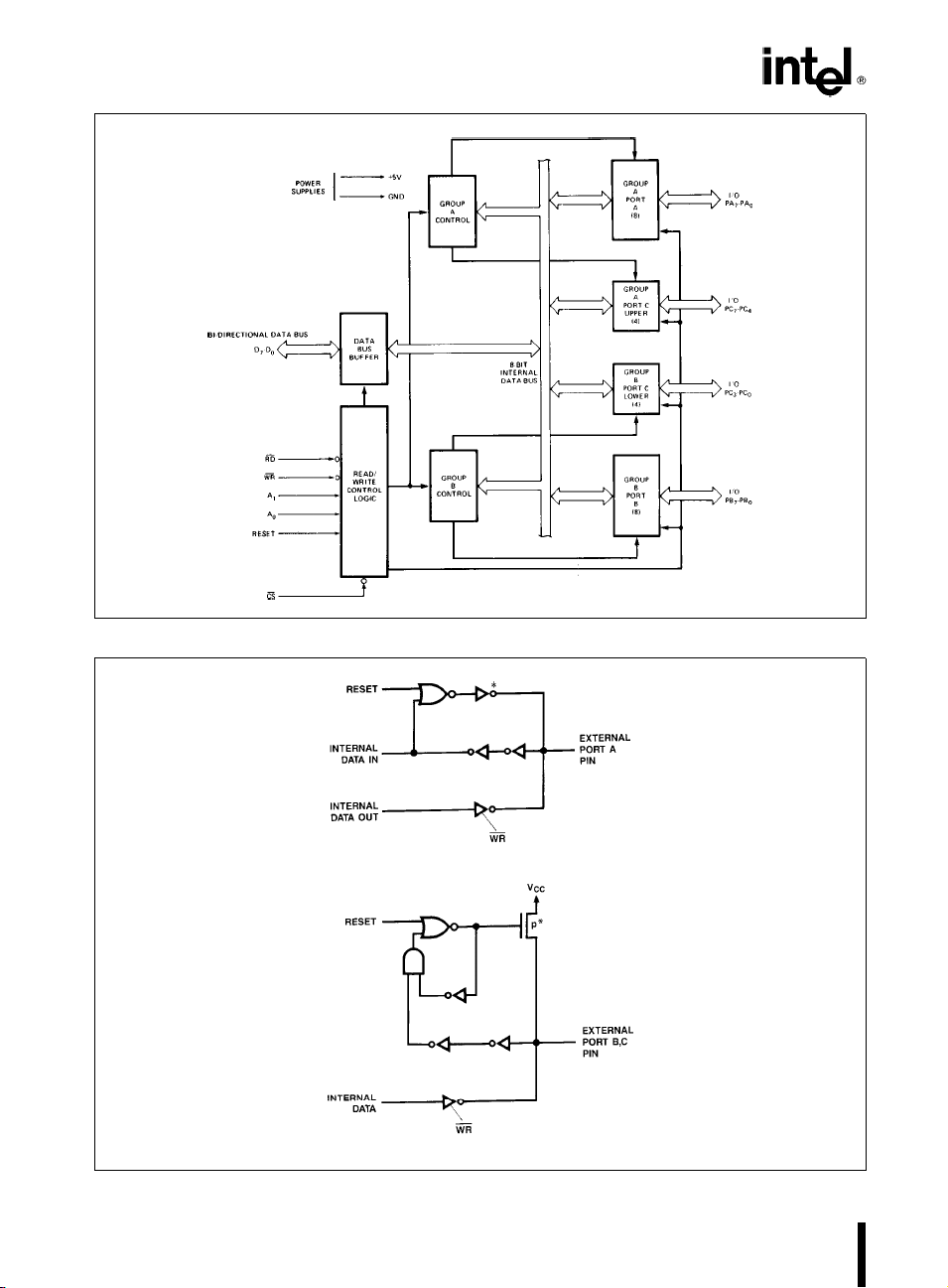
See Figure 4 for the bus-hold circuit configuration for
Port A, B, and C.
3
Page 4
82C55A
231256– 3
Figure 3. 82C55A Block Diagram Showing Data Bus Buffer and Read/Write Control Logic Functions
*NOTE: 231256– 4
Port pins loaded with more than 20 pF capacitance may not have their logic level guaranteed following a hardware reset.
Figure 4. Port A, B, C, Bus-hold Configuration
4
Page 5
82C55A OPERATIONAL DESCRIPTION
Mode Selection
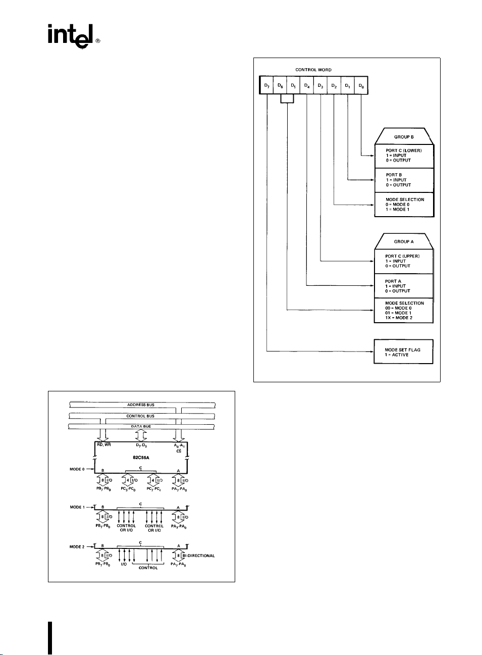
There are three basic modes of operation that can
be selected by the system software:
Mode 0 Ð Basic input/output
Mode 1 Ð Strobed Input/output
Mode 2 Ð Bi-directional Bus
When the reset input goes ‘‘high’’ all ports will be set
to the input mode with all 24 port lines held at a logic
‘‘one’’ level by the internal bus hold devices (see
Figure 4 Note). After the reset is removed the
82C55A can remain in the input mode with no additional initialization required. This eliminates the need
for pullup or pulldown devices in ‘‘all CMOS’’ designs. During the execution of the system program,
any of the other modes may be selected by using a
single output instruction. This allows a single
82C55A to service a variety of peripheral devices
with a simple software maintenance routine.
The modes for Port A and Port B can be separately
defined, while Port C is divided into two portions as
required by the Port A and Port B definitions. All of
the output registers, including the status flip-flops,
will be reset whenever the mode is changed. Modes
may be combined so that their functional definition
can be ‘‘tailored’’ to almost any I/O structure. For
instance; Group B can be programmed in Mode 0 to
monitor simple switch closings or display computational results, Group A could be programmed in
Mode 1 to monitor a keyboard or tape reader on an
interrupt-driven basis.
82C55A
231256– 6
Figure 6. Mode Definition Format
231256– 5
Figure 5. Basic Mode Definitions and Bus
Interface
The mode definitions and possible mode combinations may seem confusing at first but after a cursory
review of the complete device operation a simple,
logical I/O approach will surface. The design of the
82C55A has taken into account things such as efficient PC board layout, control signal definition vs PC
layout and complete functional flexibility to support
almost any peripheral device with no external logic.
Such design represents the maximum use of the
available pins.
Single Bit Set/Reset Feature
Any of the eight bits of Port C can be Set or Reset
using a single OUTput instruction. This feature reduces software requirements in Control-based applications.
When Port C is being used as status/control for Port
A or B, these bits can be set or reset by using the Bit
Set/Reset operation just as if they were data output
ports.
5
Page 6
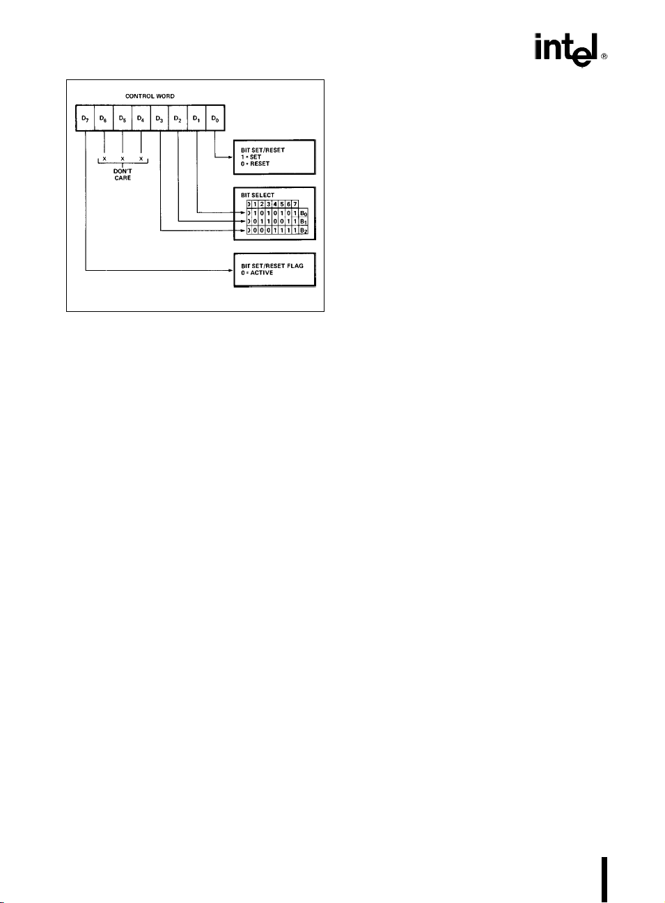
82C55A
Figure 7. Bit Set/Reset Format
231256– 7
Interrupt Control Functions
When the 82C55A is programmed to operate in
mode 1 or mode 2, control signals are provided that
can be used as interrupt request inputs to the CPU.
The interrupt request signals, generated from port C,
can be inhibited or enabled by setting or resetting
the associated INTE flip-flop, using the bit set/reset
function of port C.
This function allows the Programmer to disallow or
allow a specific I/O device to interrupt the CPU without affecting any other device in the interrupt structure.
INTE flip-flop definition:
(BIT-SET)ÐINTE is SETÐInterrupt enable
(BIT-RESET)ÐINTE is RESETÐInterrupt disable
Note:
All Mask flip-flops are automatically reset during
mode selection and device Reset.
6
Page 7
82C55A
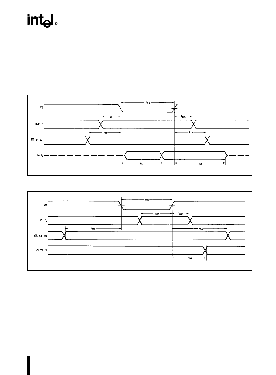
Operating Modes
Mode 0 (Basic Input/Output). This functional con-
figuration provides simple input and output operations for each of the three ports. No ‘‘handshaking’’
is required, data is simply written to or read from a
specified port.
MODE 0 (BASIC INPUT)
MODE 0 (BASIC OUTPUT)
Mode 0 Basic Functional Definitions:
Two 8-bit ports and two 4-bit ports.
#
Any port can be input or output.
#
Outputs are latched.
#
Inputs are not latched.
#
16 different Input/Output configurations are pos-
#
sible in this Mode.
231256– 8
231256– 9
7
Page 8
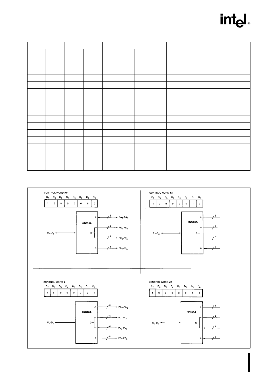
82C55A
MODE 0 Port Definition
A B GROUP A GROUP B
D
D
4
D
3
D
1
PORT A
0
PORT C
(UPPER) (LOWER)
0 0 0 0 OUTPUT OUTPUT 0 OUTPUT OUTPUT
0 0 0 1 OUTPUT OUTPUT 1 OUTPUT INPUT
0 0 1 0 OUTPUT OUTPUT 2 INPUT OUTPUT
0 0 1 1 OUTPUT OUTPUT 3 INPUT INPUT
0 1 0 0 OUTPUT INPUT 4 OUTPUT OUTPUT
0 1 0 1 OUTPUT INPUT 5 OUTPUT INPUT
0 1 1 0 OUTPUT INPUT 6 INPUT OUTPUT
0 1 1 1 OUTPUT INPUT 7 INPUT INPUT
1 0 0 0 INPUT OUTPUT 8 OUTPUT OUTPUT
1 0 0 1 INPUT OUTPUT 9 OUTPUT INPUT
1 0 1 0 INPUT OUTPUT 10 INPUT OUTPUT
1 0 1 1 INPUT OUTPUT 11 INPUT INPUT
1 1 0 0 INPUT INPUT 12 OUTPUT OUTPUT
1 1 0 1 INPUT INPUT 13 OUTPUT INPUT
1 1 1 0 INPUT INPUT 14 INPUT OUTPUT
1 1 1 1 INPUT INPUT 15 INPUT INPUT
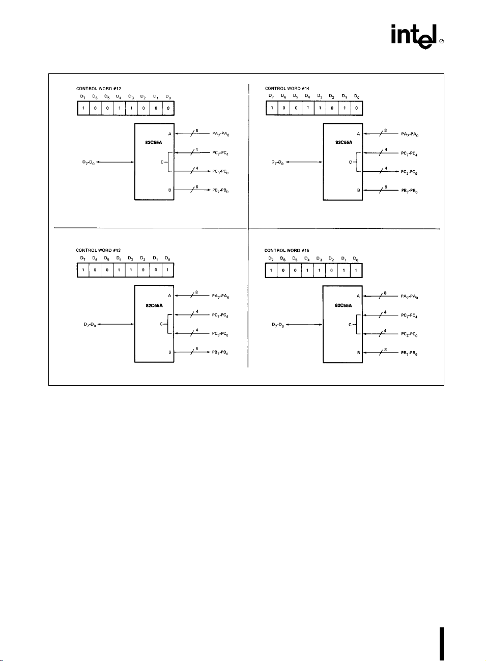
MODE 0 Configurations
Ý
PORT B
PORT C
231256– 10
8
Page 9
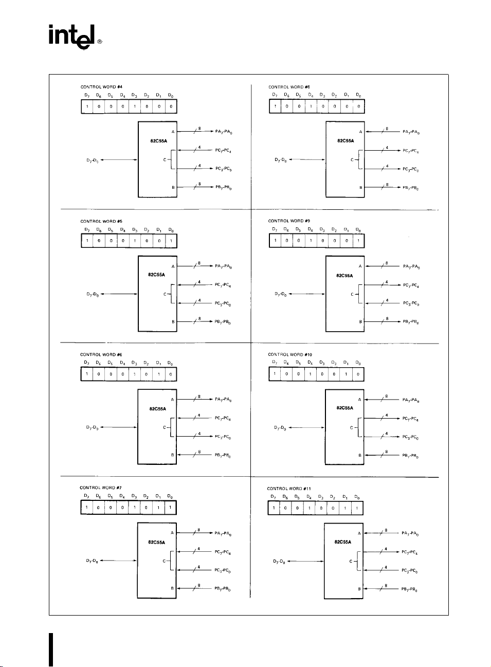
MODE 0 Configurations (Continued)
82C55A
231256– 11
9
Page 10
82C55A
MODE 0 Configurations (Continued)
Operating Modes
MODE 1 (Strobed Input/Output). This functional
configuration provides a means for transferring I/O
data to or from a specified port in conjunction with
strobes or ‘‘handshaking’’ signals. In mode 1, Port A
and Port B use the lines on Port C to generate or
accept these ‘‘handshaking’’ signals.
10
231256– 12
Mode 1 Basic functional Definitions:
Two Groups (Group A and Group B).
#
Each group contains one 8-bit data port and one
#
4-bit control/data port.
The 8-bit data port can be either input or output
#
Both inputs and outputs are latched.
The 4-bit port is used for control and status of the
#
8-bit data port.
Page 11
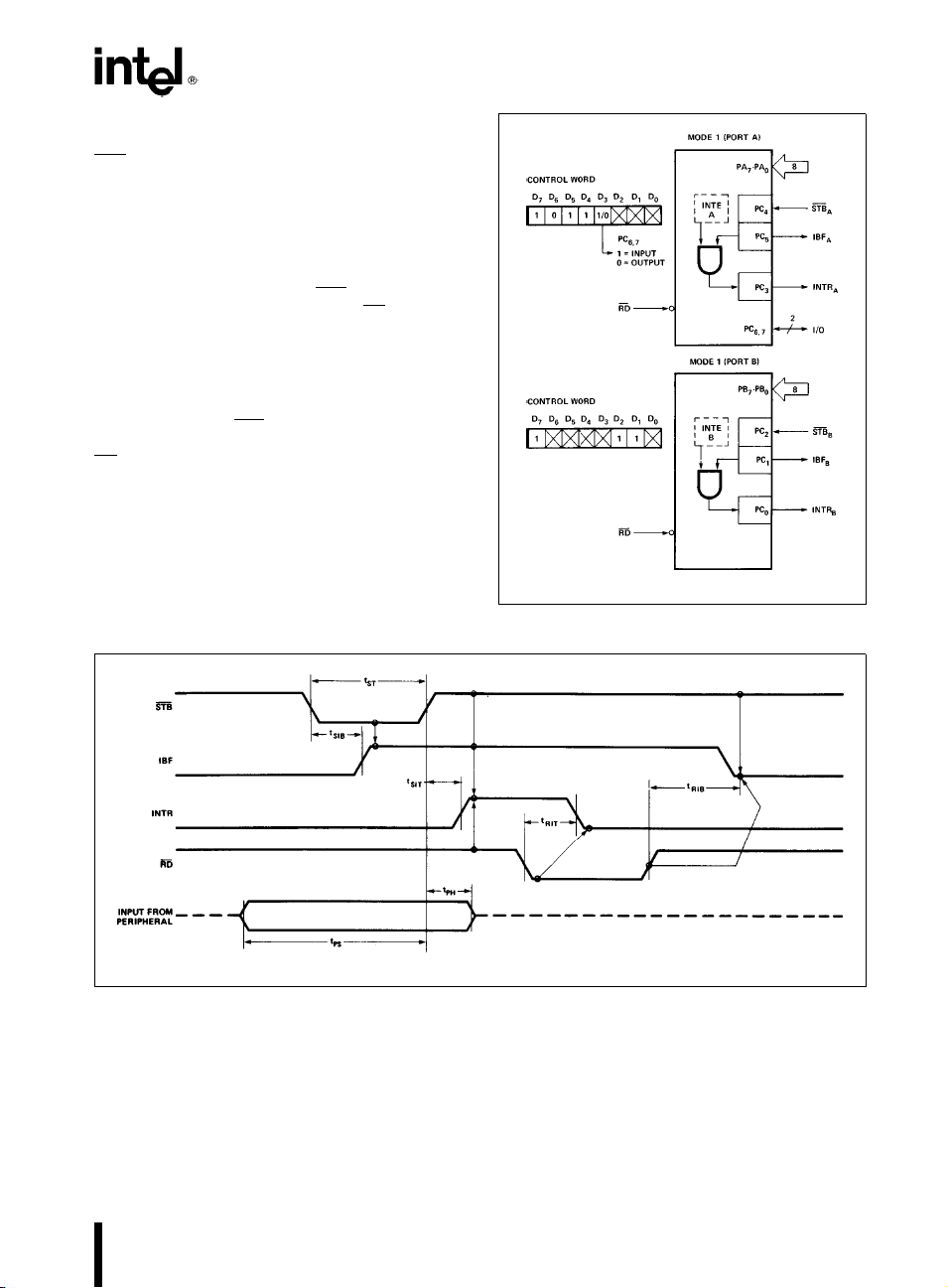
Input Control Signal Definition
STB (Strobe Input). A ‘‘low’’ on this input loads
data into the input latch.
IBF (Input Buffer Full F/F)
A ‘‘high’’ on this output indicates that the data has
been loaded into the input latch; in essence, an acknowledgement. IBF is set by STB
and is reset by the rising edge of the RD
input being low
input.
INTR (Interrupt Request)
A ‘‘high’’ on this output can be used to interrupt the
CPU when an input device is requesting service.
INTR is set by the STB
is a ‘‘one’’, IBF is a ‘‘one’’
and INTE is a ‘‘one’’. It is reset by the falling edge of
RD
. This procedure allows an input device to request service from the CPU by simply strobing its
data into the port.
INTE A
Controlled by bit set/reset of PC
.
4
INTE B
Controlled by bit set/reset of PC2.
82C55A
231256– 13
Figure 8. MODE 1 Input
Figure 9. MODE 1 (Strobed Input)
231256– 14
11
Page 12
82C55A
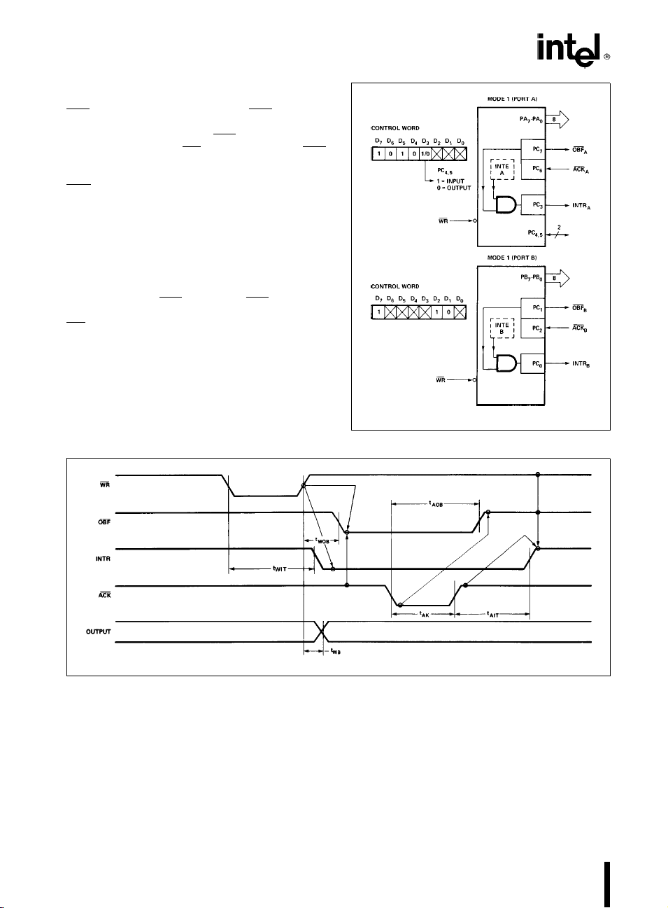
Output Control Signal Definition
OBF (Output Buffer Full F/F). The OBF output will
go ‘‘low’’ to indicate that the CPU has written data
out to the specified port. The OBF
the rising edge of the WR
Input being low.
(Acknowledge Input). A ‘‘low’’ on this input
ACK
informs the 82C55A that the data from Port A or Port
B has been accepted. In essence, a response from
the peripheral device indicating that it has received
the data output by the CPU.
INTR (Interrupt Request). A ‘‘high’’ on this output
can be used to interrupt the CPU when an output
device has accepted data transmitted by the CPU.
INTR is set when ACK
is a ‘‘one’’, OBF is a ‘‘one’’
and INTE is a ‘‘one’’. It is reset by the falling edge of
.
WR
INTE A
Controlled by bit set/reset of PC
INTE B
Controlled by bit set/reset of PC
F/F will be set by
input and reset by ACK
.
6
.
2
231256– 15
Figure 10. MODE 1 Output
12
231256– 16
Figure 11. MODE 1 (Strobed Output)
Page 13
82C55A
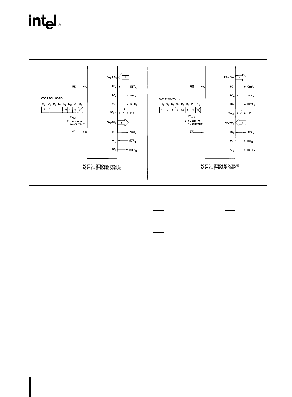
Combinations of MODE 1
Port A and Port B can be individually defined as input or output in Mode 1 to support a wide variety of strobed
I/O applications.
231256– 17
Figure 12. Combinations of MODE 1
Operating Modes
MODE 2 (Strobed Bidirectional Bus I/O).This
functional configuration provides a means for communicating with a peripheral device or structure on a
single 8-bit bus for both transmitting and receiving
data (bidirectional bus I/O). ‘‘Handshaking’’ signals
are provided to maintain proper bus flow discipline in
a similar manner to MODE 1. Interrupt generation
and enable/disable functions are also available.
MODE 2 Basic Functional Definitions:
Used in Group A only.
#
One 8-bit, bi-directional bus port (Port A) and a 5-
#
bit control port (Port C).
Both inputs and outputs are latched.
#
The 5-bit control port (Port C) is used for control
#
and status for the 8-bit, bi-directional bus port
(Port A).
Bidirectional Bus I/O Control Signal Definition
INTR (Interrupt Request). A high on this output can
be used to interrupt the CPU for input or output operations.
Output Operations
(Output Buffer Full). The OBF output will go
OBF
‘‘low’’ to indicate that the CPU has written data out
to port A.
ACK (Acknowledge). A ‘‘low’’ on this input enables
the tri-state output buffer of Port A to send out the
data. Otherwise, the output buffer will be in the high
impedance state.
INTE 1 (The INTE Flip-Flop Associated with
OBF
). Controlled by bit set/reset of PC6.
Input Operations
STB
(Strobe Input). A ‘‘low’’ on this input loads
data into the input latch.
IBF (Input Buffer Full F/F). A ‘‘high’’ on this output
indicates that data has been loaded into the input
latch.
INTE 2 (The INTE Flip-Flop Associated with IBF).
Controlled by bit set/reset of PC
.
4
13
Page 14
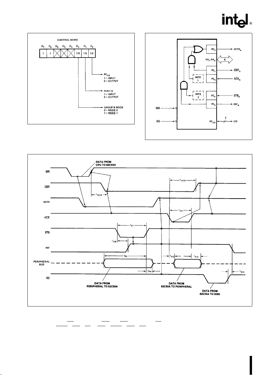
82C55A
231256– 18
Figure 13. MODE Control Word
231256– 19
Figure 14. MODE 2
NOTE:
Any sequence where WR
e
(INTR
IBF#MASK#STB#RDaOBF#MASK#ACK#WR)
14
231256– 20
Figure 15. MODE 2 (Bidirectional)
occurs before ACK, and STB occurs before RD is permissible.
Page 15
82C55A
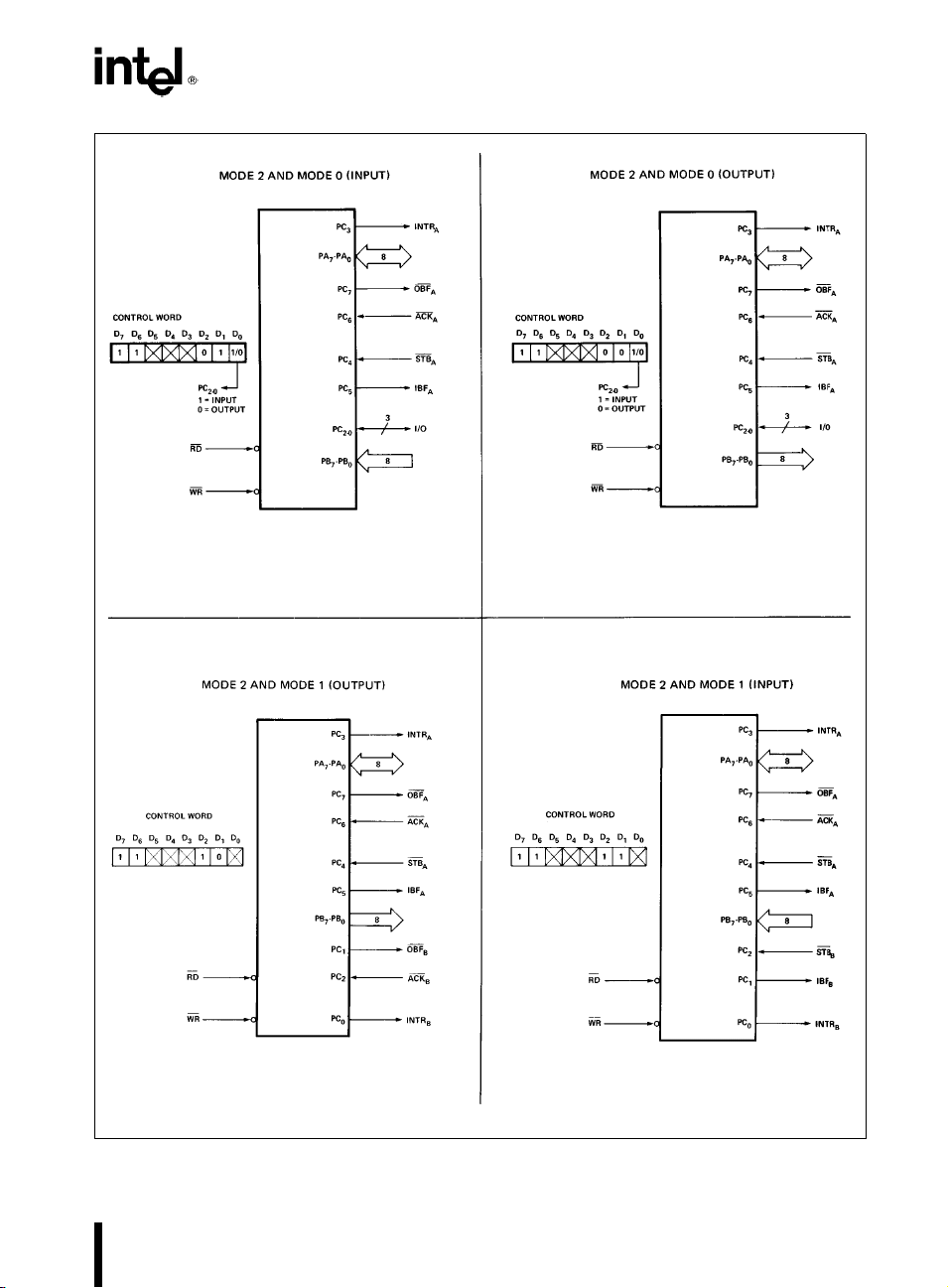
Figure 16. MODE (/4 Combinations
231256– 21
15
Page 16
82C55A
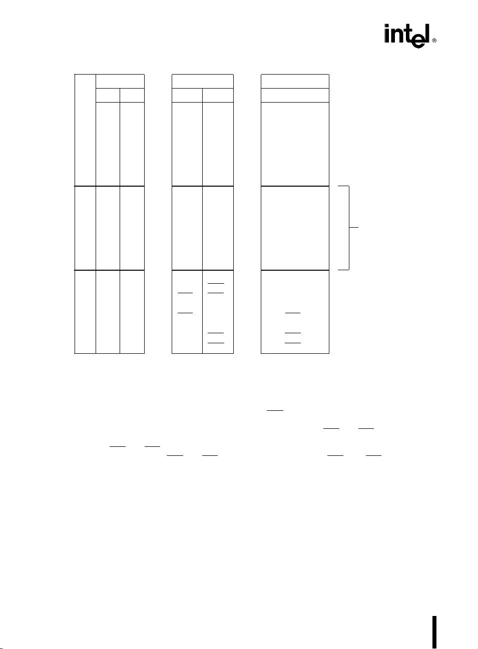
Mode Definition Summary
MODE 0 MODE 1 MODE 2
IN OUT IN OUT GROUP A ONLY
PA0IN OUT IN OUT
PA1IN OUT IN OUT
PA2IN OUT IN OUT
PA3IN OUT IN OUT
PA4IN OUT IN OUT
PA5IN OUT IN OUT
PA6IN OUT IN OUT
PA7IN OUT IN OUT
PB0IN OUT IN OUT Ð
IN OUT IN OUT Ð
PB
1
PB
IN OUT IN OUT Ð
2
PB3IN OUT IN OUT Ð
PB4IN OUT IN OUT Ð
PB
IN OUT IN OUT Ð
5
IN OUT IN OUT Ð
PB
6
PB7IN OUT IN OUT Ð
PC0IN OUT INTRBINTR
PC1IN OUT IBFBOBF
PC
IN OUT STBBACK
2
PC3IN OUT INTRAINTR
PC4IN OUT STBAI/O STB
PC5IN OUT IBF
PC6IN OUT I/O ACK
PC7IN OUT I/O OBF
A
B
B
B
A
I/O IBF
A
A
Ý
Ý
Ý
Ý
Ý
Ý
Ý
Ý
I/O
I/O
I/O
INTR
ACK
OBF
MODE 0
OR MODE 1
ONLY
A
A
A
A
A
Special Mode Combination Considerations
There are several combinations of modes possible.
For any combination, some or all of the Port C lines
are used for control or status. The remaining bits are
either inputs or outputs as defined by a ‘‘Set Mode’’
command.
During a read of Port C, the state of all the Port C
lines, except the ACK
on the data bus. In place of the ACK
states, flag status will appear on the data bus in the
PC2, PC4, and PC6 bit positions as illustrated by
Figure 18.
Through a ‘‘Write Port C’’ command, only the Port C
pins programmed as outputs in a Mode 0 group can
be written. No other pins can be affected by a ‘‘Write
Port C’’ command, nor can the interrupt enable flags
be accessed. To write to any Port C output programmed as an output in a Mode 1 group or to
16
and STB lines, will be placed
and STB line
change an interrupt enable flag, the ‘‘Set/Reset Port
C Bit’’ command must be used.
With a ‘‘Set/Reset Port C Bit’’ command, any Port C
line programmed as an output (including INTR, IBF
and OBF
can be either set or reset. Port C lines programmed
as inputs, including ACK
with Port C are not affected by a ‘‘Set/Reset Port C
Bit’’ command. Writing to the corresponding Port C
bit positions of the ACK
‘‘Set/Reset Port C Bit’’ command will affect the
Group A and Group B interrupt enable flags, as illustrated in Figure 18.
Current Drive Capability
Any output on Port A, B or C can sink or source 2.5
mA. This feature allows the 82C55A to directly drive
Darlington type drivers and high-voltage displays
that require such sink or source current.
) can be written, or an interrupt enable flag
and STB lines, associated
and STB lines with the
Page 17
82C55A
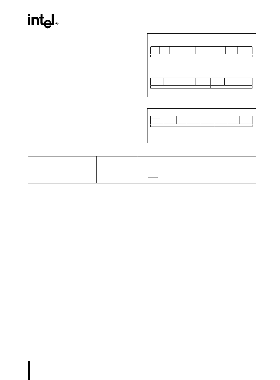
Reading Port C Status
In Mode 0, Port C transfers data to or from the peripheral device. When the 82C55A is programmed to
function in Modes 1 or 2, Port C generates or accepts ‘‘hand-shaking’’ signals with the peripheral device. Reading the contents of Port C allows the programmer to test or verify the ‘‘status’’ of each peripheral device and change the program flow accordingly.
There is no special instruction to read the status information from Port C. A normal read operation of
Port C is executed to perform this function.
D
7D6D5D4
I/O I/O IBFAINTEAINTRAINTEBIBFBINTR
D7D6D5D4D3D2D1D
OBFAINTEAI/O I/O INTRAINTEBOBFBINTR
Figure 17a. MODE 1 Status Word Format
D7D6D5D4D3D2D1D
OBFAINTE1IBFAINTE2INTR
(Defined By Mode 0 or Mode 1 Selection)
INPUT CONFIGURATION
GROUP A GROUP B
OUTPUT CONFIGURATIONS
GROUP A GROUP B
GROUP A GROUP B
D
3
A
D2D1D
Figure 17b. MODE 2 Status Word Format
Interrupt Enable Flag Position Alternate Port C Pin Signal (Mode)
INTE B PC2 ACKB(Output Mode 1) or STBB(Input Mode 1)
INTE A2 PC4 STB
INTE A1 PC6 ACK
(Input Mode 1 or Mode 2)
A
(Output Mode 1 or Mode 2
A
Figure 18. Interrupt Enable Flags in Modes 1 and 2
0
B
0
B
0
17
Page 18
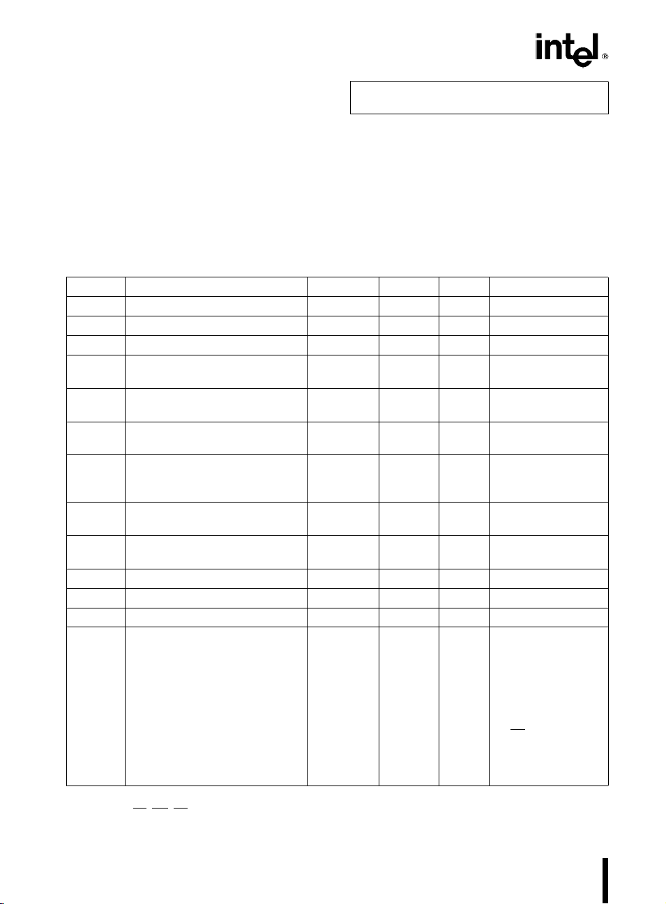
82C55A
ABSOLUTE MAXIMUM RATINGS*
Ambient Temperature Under BiasÀÀÀÀ0§Ctoa70§C
Storage Temperature АААААААААb65§Ctoa150§C
Supply Voltage АААААААААААААААААА
Operating Voltage АААААААААААААААААa4V toa7V
Voltage on any InputААААААААААGNDb2V toa6.5V
Voltage on any Output ÀÀGNDb0.5V to V
b
0.5 toa8.0V
CC
a
0.5V
NOTICE: This is a production data sheet. The specifications are subject to change without notice.
*
WARNING: Stressing the device beyond the ‘‘Absolute
Maximum Ratings’’ may cause permanent damage.
These are stress ratings only. Operation beyond the
‘‘Operating Conditions’’ is not recommended and extended exposure beyond the ‘‘Operating Conditions’’
may affect device reliability.
Power Dissipation АААААААААААААААААААААААА1 Watt
D.C. CHARACTERISTICS
e
T
0§Cto70§C, V
A
Symbol Parameter Min Max Units Test Conditions
V
IL
V
IH
V
OL
V
OH
I
IL
I
OFL
I
DAR
I
PHL
I
PHH
I
PHLO
I
PHHO
I
CC
I
CCSB
Input Low Voltage
Input High Voltage 2.0 V
Output Low Voltage 0.4 V I
Output High Voltage 3.0 V I
Input Leakage Current
Output Float Leakage Current
Darlington Drive Current
Port Hold Low Leakage Current
Port Hold High Leakage Current
Port Hold Low Overdrive Current
Port Hold High Overdrive Current
VCCSupply Current 10 mA (Note 3)
VCCSupply Current-Standby 10 mAV
CC
ea
5Vg10%, GNDe0V (T
eb
40§Ctoa85§C for Extended Temperture)
A
b
0.5 0.8 V
CC
b
V
0.4 V I
CC
g
1 mAV
V
OL
OH
OH
(Note 1)
g
10 mAV
(Note 2)
g
2.5 (Note 4) mA Ports A, B, C
R
V
a
50
a
300 mAV
Port A only
b
50
b
300 mAV
Ports A, B, C
b
350 mAV
a
350 mAV
V
Port Conditions
If I/PeOpen/High
With Data Bus
Pure Inputs
e
2.5 mA
eb
eb
e
VCCto 0V
IN
e
VCCto 0V
IN
e
500X
ext
e
1.7V
ext
e
OUT
e
OUT
e
OUT
e
OUT
e
5.5V
CC
e
VCCor GND
IN
e
O/P
High/Low
e
CS
Reset
Low/High
2.5 mA
100 mA
1.0V
3.0V
0.8V
3.0V
Open Only
High
e
Low
e
e
NOTES:
1. Pins A
2. Data Bus; Ports B, C.
3. Outputs open.
4. Limit output current to 4.0 mA.
,CS,WR,RD, Reset.
1,A0
18
Page 19
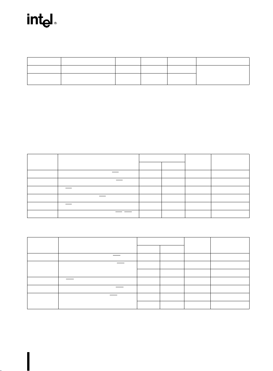
CAPACITANCE
e
T
25§C, V
A
Symbol Parameter Min Max Units Test Conditions
C
IN
C
I/O
NOTE:
5. Sampled not 100% tested.
e
GNDe0V
CC
Input Capacitance 10 pF Unmeasured plns
I/O Capacitance 20 pF
returned to GND
e
f
c
A.C. CHARACTERISTICS
e
T
0§to 70§C, V
A
eb
T
BUS PARAMETERS
READ CYCLE
40§Ctoa85§C for Extended Temperature
A
Symbol Parameter
t
AR
t
RA
t
RR
t
RD
t
DF
t
RV
ea
CC
Address Stable Before RD
Address Hold Time After RD
RD Pulse Width 150 ns
Data Delay from RD
RDuto Data Floating 10 75 ns
Recovery Time between RD/WR 200 ns
5Vg10%, GNDe0V
v
u
v
82C55A-2
Min Max
0ns
0ns
120 ns
Units
82C55A
(5)
1 MHz
Test
Conditions
WRITE CYCLE
Symbol Parameter
t
AW
t
WA
t
WW
t
DW
t
WD
Address Stable Before WR
Address Hold Time After WR
WR Pulse Width 100 ns
Data Setup Time Before WR
Data Hold Time After WR
82C55A-2
Min Max
v
u
u
u
0ns
20 ns PortsA&B
20 ns Port C
100 ns
30 ns PortsA&B
30 ns Port C
Units
Test
Conditions
19
Page 20
82C55A
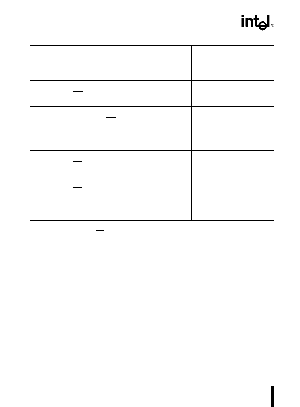
OTHER TIMINGS
Symbol Parameter
t
WB
t
lR
t
HR
t
AK
t
ST
t
PS
t
PH
t
AD
t
KD
t
WOB
t
AOB
t
SIB
t
RIB
t
RIT
t
SIT
t
AIT
t
WIT
t
RES
NOTE:
1. INTR
2. Pulse width of initial Reset pulse after power on must be at least 50 mSec. Subsequent Reset pulses may be 500 ns
minimum. The output Ports A, B, or C may glitch low during the reset pulse but all port pins will be held at a logic ‘‘one’’ level
after the reset pulse.
may occur as early as WRv.
u
WRe1 to Output 350 ns
Peripheral Data Before RD 0ns
Peripheral Data After RD 0ns
ACK Pulse Width 200 ns
STB Pulse Width 100 ns
Per. Data Before STB High 20 ns
Per. Data After STB High 50 ns
ACKe0 to Output 175 ns
ACKe1 to Output Float 20 250 ns
WRe1toOBFe0 150 ns
ACKe0toOBFe1 150 ns
STBe0toIBFe1 150 ns
RDe1toIBFe0 150 ns
RDe0 to INTRe0 200 ns
STBe1 to INTRe1 150 ns
ACKe1 to INTRe1 150 ns
WRe0 to INTRe0 200 ns see note 1
Reset Pulse Width 500 ns see note 2
82C55A-2 Units
Min Max
Conditions
Test
20
Page 21
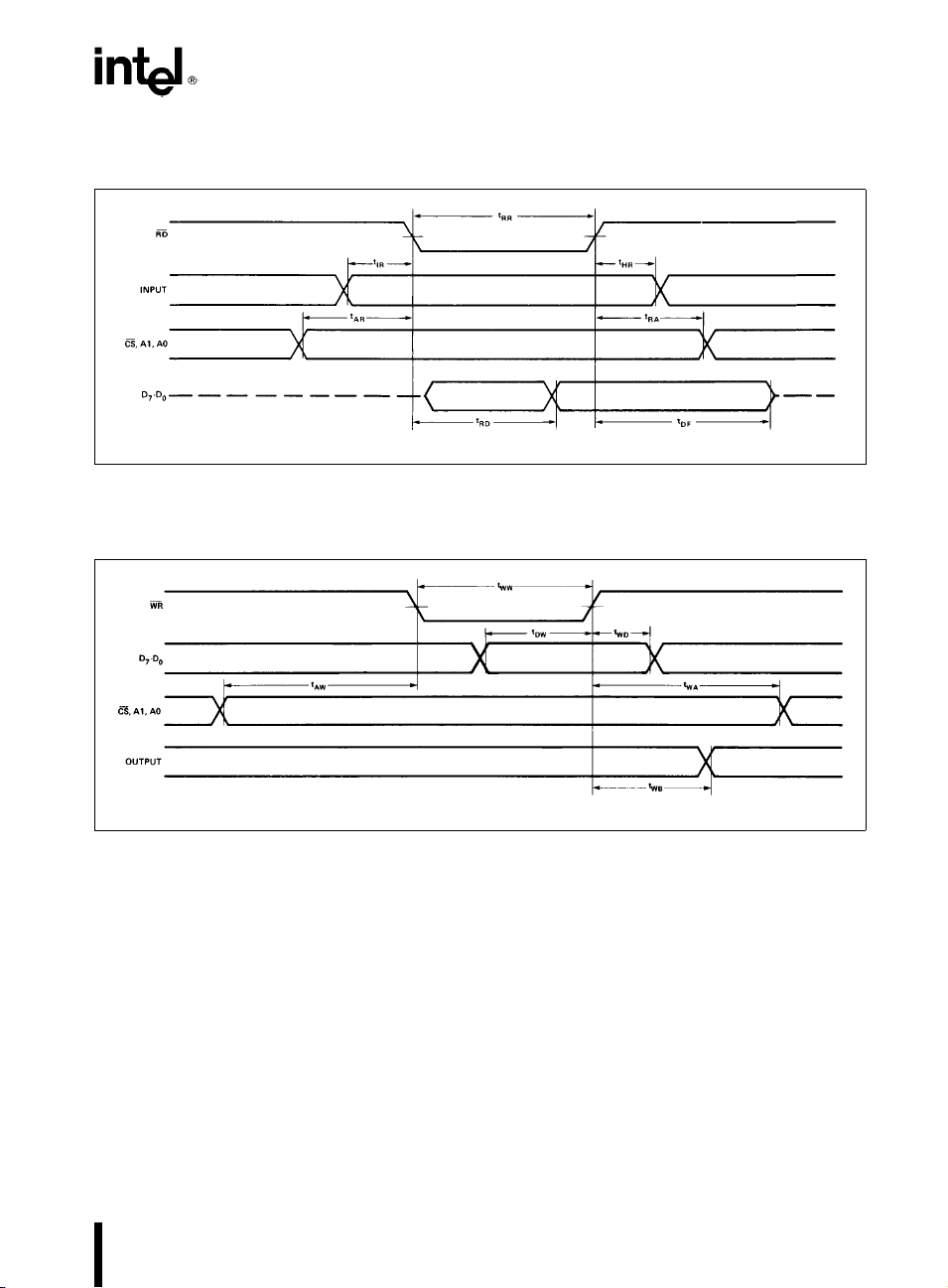
WAVEFORMS
MODE 0 (BASIC INPUT)
MODE 0 (BASIC OUTPUT)
82C55A
231256– 22
231256– 23
21
Page 22
82C55A
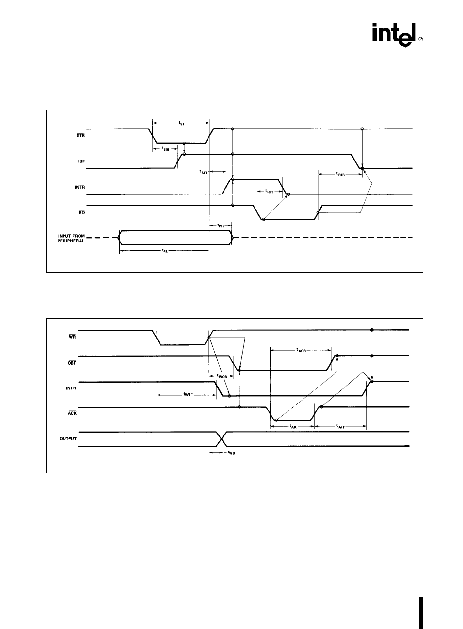
WAVEFORMS (Continued)
MODE 1 (STROBED INPUT)
MODE 1 (STROBED OUTPUT)
231256– 24
22
231256– 25
Page 23
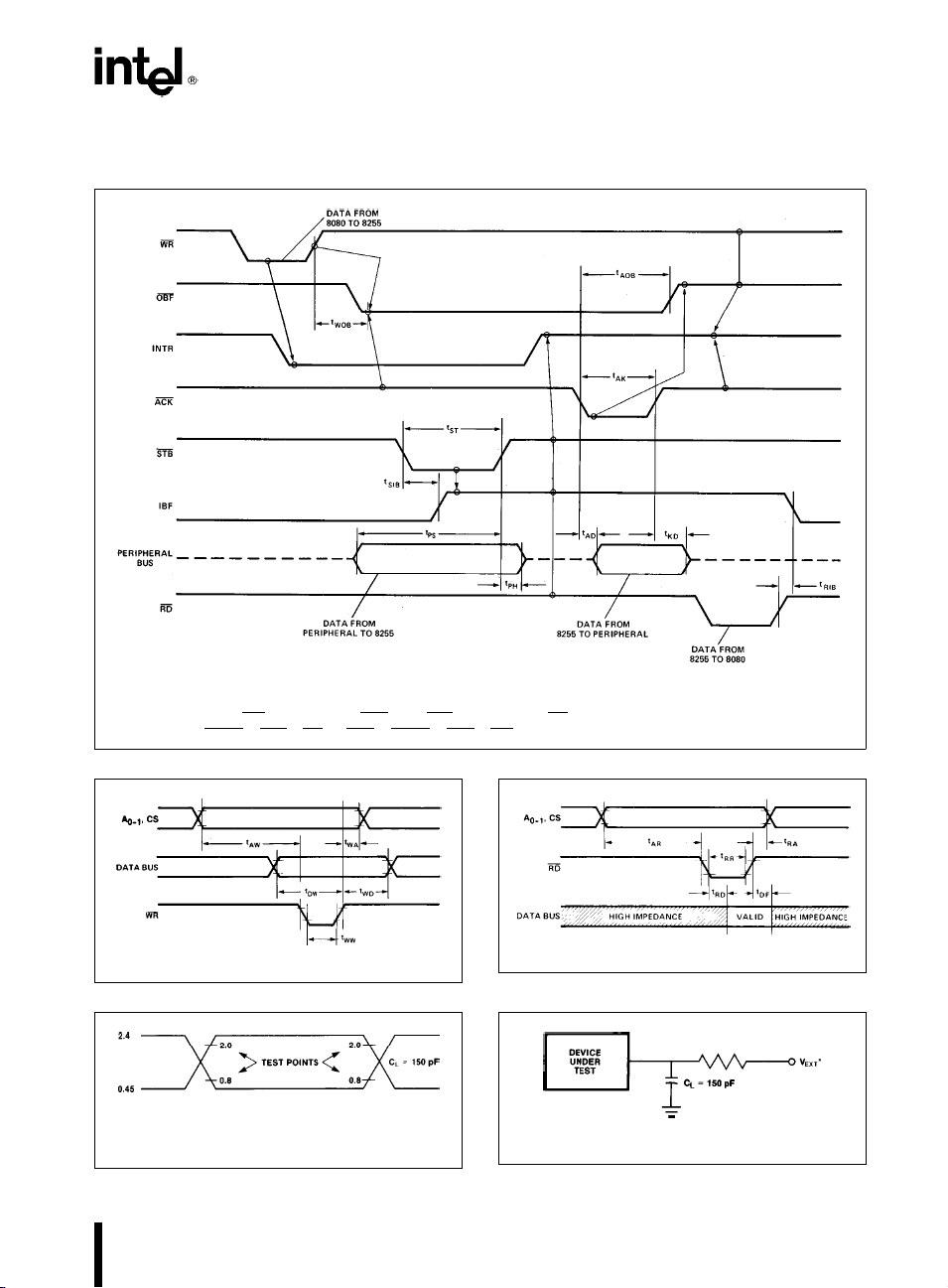
WAVEFORMS (Continued)
MODE 2 (BIDIRECTIONAL)
82C55A
Note:
Any sequence where WR
e
(INTR
IBF#MASK#STB#RDaOBF#MASK#ACK#WR)
occurs before ACK AND STB occurs before RD is permissible.
WRITE TIMING
231256– 27
A.C. TESTING INPUT, OUTPUT WAVEFORM
231256– 29
A.C. Testing Inputs Are Driven At 2.4V For A Logic 1 And 0.45V
For A Logic 0 Timing Measurements Are Made At 2.0V For A
Logic 1 And 0.8 For A Logic 0.
READ TIMING
A.C. TESTING LOAD CIRCUIT
Is Set At Various Voltages During Testing To Guarantee
*V
EXT
The Specification. CLIncludes Jig Capacitance.
231256– 26
231256– 28
231256– 30
23
 Loading...