

Page 1
PRELIMINARY
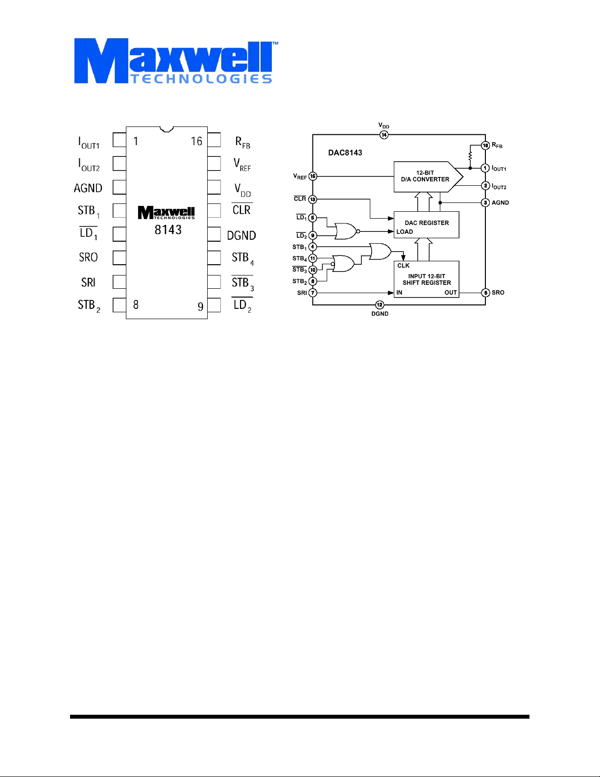
8143
12-Bit Serial Daisy Chain D/A
Converter
Memory
Logic Diagram
FEATURES:
• Microprocessor interfacing in serially controlled systems
• Buffered digital output pin for daisy-chaining multiple DACs
• Minimizes address-decoding in multiple DAC systems three wire interface for any number of DACs
- One data line
- One CLK line
- One load line
• Fast interface timing reduces timing design considerations
while minimizing microprocessor wait states.
• Improved resistance to ESD
•R
AD-PAK® radiation-hardened against natural space
radiation
• Total dose hardness:
- > 50 Krad (Si), depending upon space mission
• Package:
- 16 pin R
• Operating temperature: -40 to 85°C
AD-PAK® flat pack
DESCRIPTION:
Maxwell Technologies’ 8143 is a 12-bit serial-input daisy-chain
CMOS digital-to-analog converter (DAC) that features serial
data input and buffered serial data output and a greater than
50 krad (Si) total dose tolerance, dependent upon space mission. It was designed for multiple serial DAC systems, where
serially daisy-chaining one DAC after another is greatly simplified. The 8143 also minimizes address decoding lines
enabling simpler logic interfacing. It allows three-wire interface
for any number of DACs: one data line, one CLK line and one
load line. Serial data in the input register (MSB first) is
sequentially clocked out to the SRO pin as the new data word
(MSB first) is simultaneously clocked in from the SRI pin. The
strobe inputs are used to clock in/out data on the rising or falling (user selected) strobe edges (STB
When the shift register’s data has been updated, the new data
word is transferred to the DAC register with use of LO1 and
LD2 inputs.
Maxwell Technologies' patented R
ogy incorporates radiation shielding in the microcircuit package. It eliminates the need for box shielding while providing
the required radiation shielding for a lifetime in orbit or space
mission. In a GEO orbit, R
krad (Si) radiation dose tolerance. This product is available
with screening up to Class S.
AD-PAK provides greater than 50
, STB2, STB3, STB4).
1
AD-PAK® packaging technol-
1000599
(858) 503-3300- Fax: (858) 503-3301- www.maxwell.com
12.19.01 Rev 1
All data sheets are subject to change without notice
©2001 Maxwell Technologies
All rights reserved.
1
Page 2
12-Bit Serial Daisy-Chain D/A Converter
TABLE 1. 8143 PINOUT DESCRIPTION
PRELIMINARY
PIN SYMBOL DESCRIPTION
8143
1I
2I
OUT1
OUT2
Analog Out 1
Analog Out 2
3 AGND Analog Ground
4STB
5LD
Strobe 1
1
DAC Register Load 1
1
6 SRO Serial Data Out
7 SRI Serial Data In
8 STB2 Strobe 2
9R
10 V
11 V
FB
REF
DD
Feedback
Vlotage Reference
Positive Supply
12 CLR DAC Register Clear
13 DGND Digital Ground
14 STB
15 STB
16 LD
Strobe 4
4
Strobe 3
3
DAC Register Load 2
2
TABLE 2. 8143 ABSOLUTE MAXIMUM RATINGS
Memory
PARAMETER SYMBOL MIN MAX UNIT
VDD to DGND -- 17 V
V
to DGND -25 25 V
REF
V
to DGND -25 25 V
RFB
AGND to DGND -- V
DGND to AGND -- V
Digital Input Voltage Range -0.3 V
Output Voltage (Pin 1, Pin 2) -0.3 V
Operating Temperature Range T
Thermal Impedance
Storage Temperature T
Lead Temperature (Soldering, 60 sec) T
1000599
12.19.01 Rev 1
A
Θ
JC
STG
L
All data sheets are subject to change without notice
-40 85
-- 14.13
-65 150
-- 300
+ 0.3 V
DD
+ 0.3 V
CC
DD
DD
°
C/W
V
V
°
C
°
C
°
C
2
©2001 Maxwell Technologies.
All rights reserved.
Page 3

12-Bit Serial Daisy-Chain D/A Converter
TABLE 3. 8143 ELECTRICAL CHARACTERISTICS
(@ VDD = 5V, V
PRELIMINARY
P
ARAMETER SYMBOL CONDITIONS MIN TYP MAX UNIT
STATIC ACCURACY
Resolution N 12 -- -- Bits
Nonlinearity INL -- -- ±1 LSB
Differential Nonlinearity
Gain Error
2
Gain Tempco (DGain/DTemp)
Power Supply Rejection Ratio
(DGain/DVDD)
Output Leakage Current
Zero Scale Error
Input Resistance
AC PERFORMANCE
Output Current Settling Time
AC Feed through Error (V
3,9
I
)
OUT1
Digital-to-Analog Glitch Energy
Total Harmonic Distortion
Output Noise Voltage Density
DIGITAL INPUTS/OUTPUTS
Digital Input HIGH V
Digital Input LOW V
Input Leakage Current
Input Capacitance C
Digital Output High V
Digital Output Low V
ANALOG OUTPUTS
Output Capacitance
Output Capacitance
= 10V; V
REF
5,6
7
3
3
= V
OUT1
1
3
= V
OUT2
DNL -- -- ±1 LSB
G
FSE
TC
GFS
PSRR DV
4
REF
3,8
to
3,10
I
LKGTA
I
ZSETA
R
IN
t
S
FT V
QV
= V
AGND
R
ATINGS, UNLESS OTHERWISE SPECIFIED)
= 0V; TA = FULL TEMPERATURE RANGE SPECIFIED UNDER ABSOLUTE MAXIMUM
DGND
-- -- ±2 LSB
-- -- ±5 ppm/°C
= ±5% -- ±0.0006 ±0.002 %/%
DD
= 25°C
T
= Full Temperature Range
A
= 25°C
T
= Full Temperature Range
A
V
Pin 7 11 15 kΩ
REF
--
--
--
--
--
--
±0.002
±0.01
±5
±25
±0.03
±0.15
-- 0.380 1 µs
= 20V p-p @ f = 10 KHz, TA =
REF
°
25
C
REF
= 0V, I
load = 100 Ω, C
OUT
EXT
=
-- -- 2.0 mV p-p
-- -- 20 nVs
13 pF
3
3,11
12
THD V
= 6V rms @ 1 KHz
REF
DAC register loaded with all 1s
en10 Hz to 100 KHz between RFB and
I
OUT
IH
IL
I
VIN = 0V to 5V -- -- ±1 µA
IN
VIN = 0V -- -- 8 pF
IN
OHIOH
OLIOL
C
OUT1
C
OUT2
C
OUT1
C
OUT2
= -200 µA 4 -- -- V
= 1.6 mA -- -- 0.4 V
Digital Inputs = All 1s
Digital Inputs = All 0s
Digital Inputs = All 0s
Digital Inputs = All 1s
--
--
--
--
--
-92
-- -- 13 nV/√Hz
2.4 -- -- V
-- -- 0.8 V
--
--
--
--
--
--
--
--
90
90
60
60
8143
nA
Memory
LSB
dB
pF
pF
1000599
12.19.01 Rev 1
All data sheets are subject to change without notice
©2001 Maxwell Technologies.
All rights reserved.
3
Page 4
12-Bit Serial Daisy-Chain D/A Converter
TABLE 3. 8143 ELECTRICAL CHARACTERISTICS
(@ VDD = 5V, V
PRELIMINARY
P
ARAMETER SYMBOL CONDITIONS MIN TYP MAX UNIT
TIMING CHARACTERISTICS
Serial Input to Strobe Setup Times
(t
= 80 ns) t
STB
= 10V; V
REF
OUT1
3
= V
OUT2
t
t
t
t
t
= V
DS1
DS2
DS3
DS4
DH1
DH2
= V
AGND
DGND
R
ATINGS, UNLESS OTHERWISE SPECIFIED)
STB1 used as the strobe
STB
used as the strobe
2
STB
used as the strobe TA = 25 °C
3
T
= full temperature range
A
STB
used as the strobe
4
STB
used as the strobe TA = 25 °C
1
T
= full temperature range
A
STB
used as the strobe TA = 25 °C
2
T
= full temperature range
A
= 0V; TA = FULL TEMPERATURE RANGE SPECIFIED UNDER ABSOLUTE MAXIMUM
50
20
10
20
20
40
50
50
--
--
--
--
--
--
--
--
8143
ns
--
--
--
--
--
--
--
--
Serial Input to Strobe Hold Times
(t
= 80 ns) t
STB
STB to SRO Propagation Delay
13
SRI Data Pulsewidth t
STB
Pulsewidth (STB1 = 80 ns)
1
STB
Pulsewidth (STB2 = 100 ns) t
2
STB
Pulsewidth (STB3 = 80 ns) t
3
STB
Pulsewidth (STB4 = 80 ns) t
4
Load Pulsewidth t
14
t
LD1
LSB Strobe into Input Register to
Load DAC Register Time
CLR Pulsewidth t
POWER SUPPLY CHARACTERISTICS
Supply Voltage V
Supply Current I
Power Dissipation P
STB3 used as the strobe
DH3
STB
t
DH4
t
PD
SRI
STB1
STB2
STB3
STB4
, t
t
ASB
CLR
DD
DD
LD2TA
used as the strobe
4
TA = 25 °C
T
= full temperature range
A
= 25 °C
T
= temperature range
A
All digital inputs = VIH or V
All digital inputs = 0V or V
Digital inputs = 0V or VDD, 5V x 0.1 mA
D
Digital inputs = V
or VIL, 5V x 2 mA
IH
DD
60
--
--
Memory
ns
80
80
--
--
--
--
--
--
--
--
220
300
ns
100 -- -- ns
80 -- -- ns
80 -- -- ns
80 -- -- ns
80 -- -- ns
140
180
--
--
--
ns
--
0----ns
80 -- -- ns
4.75 5 5.25 V
IL
--
--
--
--
--
--
--
--
2
0.1
0.5
10
mA
mW
1. All grades are monotonic to 12 bits over temperature.
2. Using internal feedback resistor.
3. Guaranteed by design and not tested.
4. Applies to I
5. V
= 10V, all digital inputs = 0V.
REF
1000599
; all digital inputs = VIL, V
OUT
= 10V; specification also applied for I
REF
12.19.01 Rev 1
when all digital inputs = VIH.
OUT2
All data sheets are subject to change without notice
©2001 Maxwell Technologies.
All rights reserved.
4
Page 5
12-Bit Serial Daisy-Chain D/A Converter
8143
6. Calculated from worst case R
7. Absolute temperature coefficient is less than 300 ppm/
8. I
, Load = 100 Ω. C
OUT
9t, where t equals measured time constant of the final RC decay.
PRELIMINARY
9. All digital inputs = 0V.
10.V
= 0V, all digital inputs = 0V to VDD or VDD to 0V.
REF
11.Calculations from e
K = Boltzmann constant, J/KR = resistance
T = resistor temperature, K R = bandwidth, Hz
12.Digital input are CMOS gates; I
13.Measured from active strobe edge (STB) to new data output at SRO; C
14.Minimum low time pulsewidth for STB
EXT
= ÷4K TRB where:
n
: I
(in LSBs) = (R
REF
ZSE
= 13 pF, digital input = 0V to VDD or VDD to 0V. Extrapolated to 1/2 LSB: ts = propagation delay (tPD) +
REF
x I
LKG
°
C.
Ω
typically 1 nA at 25 °C.
IN
, STB2, and STB4, and minimum high time pulsewidth for STB3.
1
FIGURE 1. MULTIPLE WITH THREE-WIRE INTERFACE
x 4096)/V
.
REF
= 50 pF.
L
Memory
1000599
12.19.01 Rev 1
All data sheets are subject to change without notice
©2001 Maxwell Technologies.
All rights reserved.
5
Page 6
12-Bit Serial Daisy-Chain D/A Converter
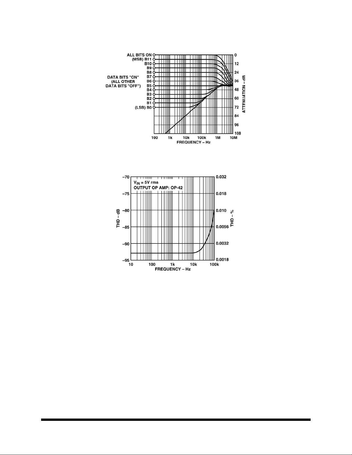
FIGURE 2. MULTIPLYING MODE FREQUENCY RESPONSE VS. DIGITAL CODE
PRELIMINARY
FIGURE 3. MULTIPLYING MODE TOTAL HARMONIC DISTORTION VS. FREQUENCY
8143
Memory
1000599
12.19.01 Rev 1
All data sheets are subject to change without notice
©2001 Maxwell Technologies.
All rights reserved.
6
Page 7

12-Bit Serial Daisy-Chain D/A Converter
FIGURE 4. SUPPLY CURRENT VS. LOGIC INPUT VOLTAGE
PRELIMINARY
FIGURE 5. LINEARITY ERROR VS. DIGITAL CODE
8143
Memory
1000599
12.19.01 Rev 1
All data sheets are subject to change without notice
©2001 Maxwell Technologies.
All rights reserved.
7
Page 8
12-Bit Serial Daisy-Chain D/A Converter
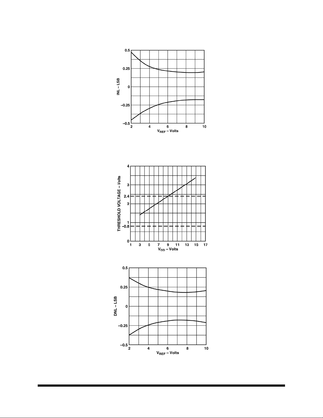
FIGURE 6. LINEARITY ERROR VS. REFERENCE VOLTAGE
PRELIMINARY
FIGURE 7. LOGIC THRESHOLD VOLTAGE VS. SUPPLY VOLTAGE
8143
Memory
1000599
FIGURE 8. DNL ERROR VS. REFERENCE VOLTAGE
12.19.01 Rev 1
All data sheets are subject to change without notice
8
©2001 Maxwell Technologies.
All rights reserved.
Page 9

12-Bit Serial Daisy-Chain D/A Converter
FIGURE 9. DIGITAL OUTPUT VOLTAGE VS. OUTPUT CURRENT
PRELIMINARY
Definition of Specifications
The resolution of a DAC is the number of states (2
where “n” is equal to the number of bits.
n
) into which the full-scale range (FSR) is divided (or resolved),
8143
Memory
Settling Time
Time required for the analog output of the DAC to settle to within 1/2 LSB of its final value for a given digital input stimulus; i.e., zero to full-scale.
Gain
Ratio of the DAC’s external operational amplifier output voltage to the V
HIGH.
Feedthrough Error
Error caused by capacitive coupling from V
Output Capacitance
Capacitance from I
Output Leakage Current
Current appearing at I
General Circuit Information
The 8143 is a 12-bit serial-input, buffered serial-output, multiplying CMOS D/A converter. It has an R-2R resistor ladder network, a 12-bit input sift register, 12-bit DAC register, control logic circuitry, and a buffered digital output stage.
The control logic forms an interface in which serial data is loaded, under microprocessor control, into the input sift register and then transferred, in parallel, to the DAC register. In addition, buffered serial output data is present at the SRO
pin when input data is loaded into the input register. This buffered data follows the digital input data (SRI) by 12 clock
cycles and is available for daisy-chaining additional DACs.
to ground.
OUT1
when all digital inputs are LOW, or at IOUT2 terminal when all inputs are HIGH.
OUT1
to output. Feedthrough error limits are specified with all switches off.
REF
input voltage when all digital inputs are
REF
1000599
12.19.01 Rev 1
All data sheets are subject to change without notice
©2001 Maxwell Technologies.
All rights reserved.
9
Page 10

12-Bit Serial Daisy-Chain D/A Converter
An asynchronous CLEAR function allows resetting the DAC register to a zero code (0000 0000 0000) without altering
data stored in the registers.
A simplified circuit of the 8143 is shown in Figure 10. An inverses R-2R ladder network consisting of silicon-chrome,
PRELIMINARY
thin-film resistors, and twelve pairs of NMOS current-steering switches. These switches steer binarily weighted currents into either I
less of digital input code. This constant current results in a constant input resistance at V
Ω). The V
k
Absolute Maximum Ratings chart.
The twelve output current-steering switches are in series with the R-2R resistor ladder, and therefore, can introduce bit
errors. It was essential to design these switches such that the switch “ON” resistance by binarily scaled so that the
voltage drop across each switch remains constant. If, for example, Switch 1 of Figure 10 was designed with an “ON”
resistance of 10
To further ensure accuracy across the full temperature range, permanently “ON” MOS switches were included in
series with the feedback resistor and the R-2R ladder’s terminating resistor. The Simplified DAC Circuit, Figure 10,
shows the location of these switches. These series switches are equivalently scaled to two times Switch 1 (MSB) and
top Switch 12 (LSB) to maintain constant relative voltage drops with varying temperature. During any testing of the
resistor ladder or R
REF
or I
OUT1
input may be driven by any reference voltage or current, ac or dc, that is within the limits stated in the
. Switching current to I
OUT2
OUT1
or I
yields a constant current in each ladder leg, regard-
OUT2
equal to R (typically 11
REF
Ω, Switch 2 for 20 Ω, etc., a constant 5 mV drop would then be maintained across each switch.
FEEDBACK
(such as incoming inspection), VDD must be present to turn “ON” these serial switches.
FIGURE 10. SIMPLIFIED DAC CIRCUIT
8143
Memory
ESD Protection
The 8143 digital inputs have been designed with ESD resistance incorporated through careful layout and the inclusion
of input protection circuitry.
Figure 11 shows the input protection diodes. High voltage static charges applied to the digital inputs are shunted to the
supply and ground rails through forward biased diodes.
These protection diodes were designed to clamp the inputs well below dangerous levels during static discharge conditions.
1000599
12.19.01 Rev 1
All data sheets are subject to change without notice
©2001 Maxwell Technologies.
All rights reserved.
10
Page 11

12-Bit Serial Daisy-Chain D/A Converter
FIGURE 11. DIGITAL INPUT PROTECTION
PRELIMINARY
Equivalent Circuit Analysis
8143
Figures 12 and 13 show equivalent circuits for the 8143 internal DAC with all bits LOW and HIGH, respectively. The
reference current is switched to IOUT2 when all data bits are LOW, and to IOUT1 when all bits are HIGH. The ILEAKAGE current source is the combination of surface and junction leakages to the substrate. The 1/4096 current source
represents the constant 1-bit current drain, through the ladder’s terminating resistor.
Output capacitance is dependent upon the digital input code. This is because the capacitance of a MOS transistor
changes with applied gate voltage. This output capacitance varies between the low and high values.
FIGURE 12. EQUIVALENT CIRCUIT (ALL INPUTS LOW)
Memory
1000599
12.19.01 Rev 1
All data sheets are subject to change without notice
©2001 Maxwell Technologies.
All rights reserved.
11
Page 12

12-Bit Serial Daisy-Chain D/A Converter
FIGURE 13. EQUIVALENT CIRCUIT (ALL INPUT HIGH)
PRELIMINARY
Dynamic Performance
Analog Output Impedance
The output resistance, as in the case of the output capacitance, varies with the digital input code. This resistance,
looking back into the IOUT1 terminal, varies between 11 kW (the feedback resistor alone when all digital input are
LOW) and 7.5 k
when any single bit logic is HIGH). Static accuracy and dynamic performance will be affected by these variations.
The gain and phase stability of the output amplifier, board layout, and power supply decoupling will all affect the
dynamic performance of the 8143. The use of a small compensation capacitor may be required when high speed
operational amplifier’s feedback resistor to provide the necessary phase compensation to critically damp the output.
The considerations when using high speed amplifiers are:
1. Phase compensation (see Figures 16 and 17).
2. Power supply decoupling at the device socket and use of proper grounding techniques.
Ω (the feedback resistor in parallel with approximately 30 kΩ of the R-2R ladder network resistance
8143
Memory
Output Amplifier Considerations
When using high speed op amps, a small feedback capacitor (typically 5 pF-30 pF) should be used across the amplifiers to minimize overshoot and ringing. For low speed or static applications, ac specification of the amplifier are not
very critical. In high speed applications, slew rate, settling time, open-loop gain and gain/phase margin specifications
of the amplifier should be selected for the desired performance. It has already been noted that an offset can be caused
by including the usual bias current compensation resistor in the amplifier’s noninverting input terminal. This resistor
should not be used. Instead, the amplifier should have a bias current that is low over the temperature range of interest.
Static accuracy is affected by the variation in the DAC’s output resistance. This variation is best illustrated by using the
circuit of Figure 14 and the equation:
1000599
12.19.01 Rev 1
All data sheets are subject to change without notice
©2001 Maxwell Technologies.
All rights reserved.
12
Page 13

12-Bit Serial Daisy-Chain D/A Converter
FIGURE 14. SIMPLIFIED CIRCUIT
PRELIMINARY
Where RO is a function of the digital code, and:
R
= 10 kΩ for more than four bits of Logic 1,
O
= 30 kΩ for any single bit of Logic 1.
R
O
8143
Memory
Therefore, the offset gain varies as follows:
at code 00 11 1111 1111,
at code 0100 0000 0000,
The error difference is 2/3 V
Since one LSB has a weight (for V
using either the amplifier’s pulling pins, an external pulling network, or by selection of an amplifier with inherently low
. Amplifiers with sufficiently low VOS include OP77, OP07 and OP27.
V
OS
Interface Logic Operation
The microprocessor interface of the 8143 has been designed with multiple STROBE and LOAD inputs to maximize
interfacing options. Control signals decoding may be done on chip or with the use of external decoding circuitry (see
Figure 21).
Serial data is clocked into the input register and buffered output stage with STB
active on the rising edge. STB
Serial data output (SRO) follows the serial data input (SRI) by 12 clocked bits.
Holding any STROBE input at its selected state (i.e., STB
to prevent any further data input.
When a new data word has been entered into the input register, it is transferred to the DAC register by asserting both
LOAD inputs.
.
OS
= 10V) of 2.4 mV for the 8143, it is clearly important that VOS be minimized,
REF
may be used with a falling edge clock data.
3
, STB2, or STB4 at logic HIGH or STB3 at logic LOW) will act
1
, STB2, or STB4. The strobe inputs are
1
1000599
12.19.01 Rev 1
All data sheets are subject to change without notice
©2001 Maxwell Technologies.
All rights reserved.
13
Page 14

12-Bit Serial Daisy-Chain D/A Converter
The CLR input allows asynchronous resetting of the DAC register to 0000 0000 0000. This reset does not affect data
held in the input registers. While in unipolar mode, a CLEAR will result in the analog output going to 0V. In bipolar
mode, the output will go to -V
REF
.
PRELIMINARY
Interface Input Description
STB
(Pin 4), STB2 (Pin 8), STB4 (Pin 11) - Input register and buffered output strobe. Inputs active on falling edge.
1
Selected to load serial data into input register and buffered output stage. See Table 3 for details.
(Pin 10) - Input register and buffered output strobe input. Active on falling edge. Selected to load serial data into
STB
3
input register and buffered output stage. See Table 3 for details.
LD
(Pin 5), LD2 (Pin 9) - Load DAC register inputs. Active low. Selected together to load contents of input register into
1
DAC register.
CLR
(Pin 13) - Clear input. Active low. Asynchronous. When LOW, 12-bit DAC register is forced to a zero code (0000
0000 0000) regardless of other interface inputs.
FIGURE 15. TIMING DIAGRAM
8143
Memory
* Strobe waveform is inverted if STB3 is used to strobe serial data bits into input register.
** Data is strobed into and out of the input shift register MSB first.
TABLE 1. TRUTH TABLE
INPUT REGISTER/DIGITAL
O
UTPUT
STB4 STB3 STB2 STB1 CLR LD2 LD1
0
0
0
1000599
1
1
1
CONTROL INPUTS
0
0
0
0
0
0
DAC
R
EGISTER
X
X
X
X
12.19.01 Rev 1
CONTROL INPUT OPERATION
X
X
X
X
X
X
X
X
All data sheets are subject to change without notice
Serial data bit loaded from
SRI into input register and
digital output (SRO pin)
after 12 clocked bits
©2001 Maxwell Technologies.
All rights reserved.
NOTE
S
1,2
14
Page 15

12-Bit Serial Daisy-Chain D/A Converter
TABLE 1. TRUTH TABLE
8143
INPUT REGISTER/DIGITAL
O
PRELIMINARY
UTPUT
CONTROL INPUTS
DAC
R
EGISTER
CONTROL INPUT OPERATION
STB4 STB3 STB2 STB1 CLR LD2 LD1
1
X
X
X
X
0
X
X
X
X
1
X
X
X
X
1
No operation (input register
and SRO)
0 X X Reset DAC register to zero
code (Code: 0000 0000
0000) Asynchronous operations)
1
1
1
X
X
No operation (DAC register
1
and SRO)
1 0 0 Load DAC register with the
contents of input register
1. Serial data is loaded into Input Register MSB first, on edges shown. is positive edges, is negative edge.
2. 0 = Logic LOW, 1 = Logic HIGH, X = Don’t care.
3. CLR
= 0 asynchronously resets DAC register to 0000 0000 0000, but has no effect on Input Register.
Applications Information
Unipolar Operation (2-Quadrant)
The circuit shown in Figures 16 and 17 may be used with an ac or dc reference voltage. The circuit’s output will range
between 0V and 10V (4095/4096) depending upon the digital input and the analog output is shown in Table 4. The
V
voltage range is the maximum input voltage range of the op amp or ±25V, whichever is lowest.
REF
NOTE
S
2
2,3
2
2
Memory
1000599
TABLE 4. UNIPOLAR CODE TABLE
OMINAL ANALOG OUTPUT (V
DIGITAL INPUT
MSB LSB
1 1 1 1 1 1 1 1 1 1 1 1 -V
1 0 0 0 0 0 0 0 0 0 0 1 -V
1 0 0 0 0 0 0 0 0 0 0 0 -V
0 1 1 1 1 1 1 1 1 1 1 1 -V
0 0 0 0 0 0 0 0 0 0 0 1 -V
0 0 0 0 0 0 0 0 0 0 0 0 -V
N
AS SHOWN IN FIGURES 16 AND 17)
(2048/4096) = -V
REF
12.19.01 Rev 1
OUT
(4095/4096)
REF
(2049/4096)
REF
/2
REF
(2047/4096)
REF
(1/4096)
REF
(0/4096)
REF
All data sheets are subject to change without notice
©2001 Maxwell Technologies.
15
All rights reserved.
Page 16

12-Bit Serial Daisy-Chain D/A Converter
FIGURE 16. UNIPOLAR OPERATION WITH HIGH ACCURACY OP AMP (2-QUADRANT)
PRELIMINARY
IGURE 17. UNIPOLAR OPERATION WITH FAST OP AMP AND GAIN ERROR TRIMMING (2-QUADRANT)
F
8143
Memory
In many applications, the 8143 zero scale error and low gain error, permit the elimination of external trimming components without adverse effects on circuit performance.
For applications requiring a tighter gain error than 0.024% at 25
part, the circuit in Figure 17 may be used. Gain error may be trimmed by adjusting R1.
The DAC register must first be loaded with all 1s. R1 is then adjusted until V
adjustable V
Bipolar Operation (4-Quadrant)
Figure 18 details a suggested circuit for bipolar, or offset binary, operation. Table 5 shows the digital input-to-analog
output relationship. The circuit uses offset binary coding. Twos complement code can be converted to offset binary by
software inversion of the MSB or by the addition of an external inverter to the MSB input.
Resistor R3, R4 and R5 must be selected to match within 0.01% and must all be of the same (preferably metal foil)
type to assure temperature coefficient match. Mismatching between R3 and R4 causes offset and full-scale error.
Calibration is performed by loading the DAC register with 1000 0000 0000 and adjusting the ratio of R3 to R4 to yield
V
= 0V. Full scale can be adjusted by loading the DAC register with 1111 1111 1111 and adjusting either the ampli-
OUT
tude of V
1000599
, R1 and R
REF
of the value of R5 until the desired V
REF
FEEDBACK
may be omitted, with V
is achieved.
OUT
12.19.01 Rev 1
°
C for the top grade part, or 0.048% for the lower grade
= -V
adjusted to yield the desired full-scale output.
REF
OUT
All data sheets are subject to change without notice
(4095/4096). In the case of an
REF
©2001 Maxwell Technologies.
All rights reserved.
16
Page 17

12-Bit Serial Daisy-Chain D/A Converter
T
ABLE 5. BIPOLAR (OFFSET BINARY) CODE TABLE
PRELIMINARY
DIGITAL INPUT
MSB LSB
OMINAL ANALOG OUTPUT
N
(V
AS SHOWN IN FIGURE
OUT
18)
8143
1 1 1 11 1 1 11 1 1 1 V
1 0 0 00 0 0 00 0 0 1 V
1 0 0 0 0 0 0 00 0 0 0 0
0 1 1 11 1 1 11 1 1 1 -V
0 0 0 00 0 0 00 0 0 1 -V
0 0 0 00 0 0 00 0 0 0 -V
(2047/2048)
REF
(1/2048)
REF
(1/2048)
REF
(2047/2048)
REF
(2048/2048)
REF
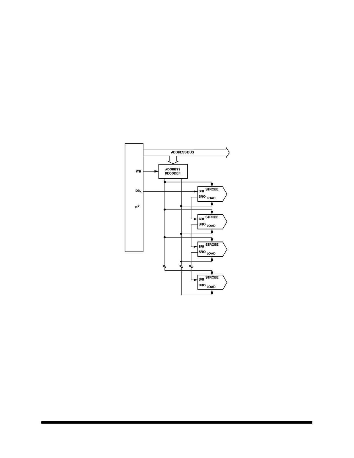
Daisy-Chaining 8143
Many applications use multiple serial input DACs that use numerous interconnecting lines for address decoding and
data lines. In addition, they use some type of buffering to reduce loading on the bus. The 8143 is ideal for just such an
application. It not only reduces the number of interconnecting lines, but also reduces bus loading. The 8143 can be
daisy-chained with only three lines: one data line, one CLK and one load line, see Figure 19.
FIGURE 18. BIPOLAR OPERATION (4-QUADRANT, OFFSET BINARY)
Memory
1000599
12.19.01 Rev 1
All data sheets are subject to change without notice
©2001 Maxwell Technologies.
All rights reserved.
17
Page 18

12-Bit Serial Daisy-Chain D/A Converter
FIGURE 19. MULTIPLE 8143S WITH THREE WIRE INTERFACE
PRELIMINARY
8143
Memory
Analog/Digital Division
The transfer function for the 8143 connect is the multiplying mode as shown in Figures 16 and 17 is:
where AX assumes a value of 1 for an “ON” bit and 0 for an “OFF” bit.
The transfer function is modified when the DAC is connected in the feedback of an operational amplifier as shown in
Figure 20 and is:
The above transfer function is the division of an analog voltage (VREF) by a digital word. The amplifier goes to the
rails with all bits “OFF” since division by zero is infinity. With all bits “ON”, the gain is 1 (±1 LSB). The gain becomes
4096 with the LSB, Bit 12, “ON”.
1000599
12.19.01 Rev 1
All data sheets are subject to change without notice
©2001 Maxwell Technologies.
All rights reserved.
18
Page 19

12-Bit Serial Daisy-Chain D/A Converter
FIGURE 20. ANALOG/DIGITAL DIVIDER
PRELIMINARY
8143
Memory
Application Tips
, I
In most applications, linearity depends on the potential of I
to each other. In most applications, the DAC is connected to an external Op Amp with its noninverting input tied to
ground (see Figures 16 and 17). The amplifier selected should have a low input bias current and low drift over temperature. The amplifier’s input offset voltage should be nulled to less than ±200 µV (less than 10% of 1 LSB).
The operational amplifier’s noninverting input should have a minimum resistance connection to ground; the usual bias
current compensation resistor should not be used. This resistor can cause a variable offset voltage appearing as a
varying output error. All grounded pins should tie to a single common ground point, avoiding ground loops. The V
power supply should have a low noise level with no transients greater than 17V.
It is recommended that the digital input be taken to ground or V
accumulation of static charge if the PC card is disconnected from the system.
Peak supply current flows as the digital input pass through the transition region (see Figure 4). The supply current
decreases as the input voltage approaches the supply rails (V
very near the supply rails will minimize supply current.
Interfacing to the MC6800
As shown in Figure, the 8143 may be interfaced to the 6800 by successively executing memory WRITE instruction
while manipulating the data between WRITEs, so that each WRITE presents the next bit.
In this example, the most significant bits are found in memory locations 0000 and 0001. The four MSBs are found in
the lower half of 0000, the eight LSBs in 0001. The data is taken from the DB
The serial data loading is triggered by STB
W
, and f2. A WRITE to another address location transfers data from input register to DAC register.
which is asserted by a decoded memory WRITE to a memory location, R/
4
OUT1
, and AGND (Pins 1, 2 and 3) being exactly equal
OUT2
via a high value (1 MΩ) resistor, this will prevent the
DD
or DGND), i.e., rapidly slewing logic signals that settle
DD
line.
7
DD
1000599
12.19.01 Rev 1
All data sheets are subject to change without notice
©2001 Maxwell Technologies.
All rights reserved.
19
Page 20

12-Bit Serial Daisy-Chain D/A Converter
FIGURE 21. MC6800 INTERFACE
PRELIMINARY
8143
Interface to the 8085
The 8143’s interface to the 8085 microprocessor is shown in Figure 22. Note that the microprocessor’s SOD line is
used to present data serially to the DAC.
Data is strobed into the 8143 by executing memory write instructions. The strobe 2 input is generated by decoding an
address location and WR
location.
Serial data supplied to the 8143 must be present in the right-justified format in registers H and L of the microprocessor.
. Data is loaded into the DAC register with a memory write instruction to another address
FIGURE 22. 8085 INTERFACE
Memory
Interface to the 68000
Figure 23 shows the 8143 configured to the 68000 microprocessor. Serial data input is similar to that of the 6800 in
Figure 21.
1000599
12.19.01 Rev 1
All data sheets are subject to change without notice
©2001 Maxwell Technologies.
All rights reserved.
20
Page 21

12-Bit Serial Daisy-Chain D/A Converter
FIGURE 23. 8143 TO 68000 µP INTERFACE
PRELIMINARY
8143
Memory
1000599
12.19.01 Rev 1
All data sheets are subject to change without notice
©2001 Maxwell Technologies.
All rights reserved.
21
Page 22

12-Bit Serial Daisy-Chain D/A Converter
PRELIMINARY
8143
Memory
16 PIN RAD-PAK® FLAT PACKAGE
SYMBOL DIMENSION
MIN NOM MAX
A 0.115 0.135 0.150
b 0.015 0.017 0.019
c 0.004 0.005 0.007
D 0.407 0.415 0.423
E 0.275 0.280 0.285
E1 -- -- 0.500
E2 0.150 0.156 0.162
E3 0.030 0.062 --
e 0.050 BSC
L 0.325 0.335 0.345
Q 0.020 0.033 0.045
S1 0.005 0.024 0.045
N16
F16-01
Note: All Dimensions in inches
1000599
12.19.01 Rev 1
All data sheets are subject to change without notice
©2001 Maxwell Technologies.
All rights reserved.
22
Page 23

12-Bit Serial Daisy-Chain D/A Converter
Important Notice:
These data sheets are created using the chip manufacturer’s published specifications. Maxwell Technologies verifies
PRELIMINARY
functionality by testing key parameters either by 100% testing, sample testing or characterization.
The specifications presented within these data sheets represent the latest and most accurate information available to
date. However, these specifications are subject to change without notice and Maxwell Technologies assumes no
responsibility for the use of this information.
Maxwell Technologies’ products are not authorized for use as critical components in life support devices or systems
without express written approval from Maxwell Technologies.
Any claim against Maxwell Technologies must be made within 90 days from the date of shipment from Maxwell Technologies. Maxwell Technologies’ liability shall be limited to replacement of defective parts.
8143
Memory
1000599
12.19.01 Rev 1
All data sheets are subject to change without notice
©2001 Maxwell Technologies.
All rights reserved.
23
Page 24

12-Bit Serial Daisy-Chain D/A Converter
)
Product Ordering Options
PRELIMINARY
Model Number
8143
8143
RP
F X
Feature
Screening Flow
Package
Option Details
Monolithic
S = Maxwell Class S
B = Maxwell Class B
E = Engineering (testing @ +25°C
I = Industrial (testing @ -55°C,
+25°C, +125°C)
F = Flat Pack
Memory
1000599
Radiation Feature
Base Product
Nomenclature
12.19.01 Rev 1
RP = R
AD-PAK® package
12-Bit Serial Daisy Chain D/A
Converter
All data sheets are subject to change without notice
©2001 Maxwell Technologies.
All rights reserved.
24
 Loading...