

Page 1
August 1990 Order Number: 231456-006
8088
8-BIT HMOS MICROPROCESSOR
8088/8088-2
Y
8-Bit Data Bus Interface
Y
16-Bit Internal Architecture
Y
Direct Addressing Capability to 1 Mbyte
of Memory
Y
Direct Software Compatibility with 8086
CPU
Y
14-Word by 16-Bit Register Set with
Symmetrical Operations
Y
24 Operand Addressing Modes
Y
Byte, Word, and Block Operations
Y
8-Bit and 16-Bit Signed and Unsigned
Arithmetic in Binary or Decimal,
Including Multiply and Divide
Y
Two Clock Rates:
Ð 5 MHz for 8088
Ð 8 MHz for 8088-2
Y
Available in EXPRESS
Ð Standard Temperature Range
Ð Extended Temperature Range
The Intel 8088 is a high performance microprocessor implemented in N-channel, depletion load, silicon gate
technology (HMOS-II), and packaged in a 40-pin CERDIP package. The processor has attributes of both 8and 16-bit microprocessors. It is directly compatible with 8086 software and 8080/8085 hardware and peripherals.
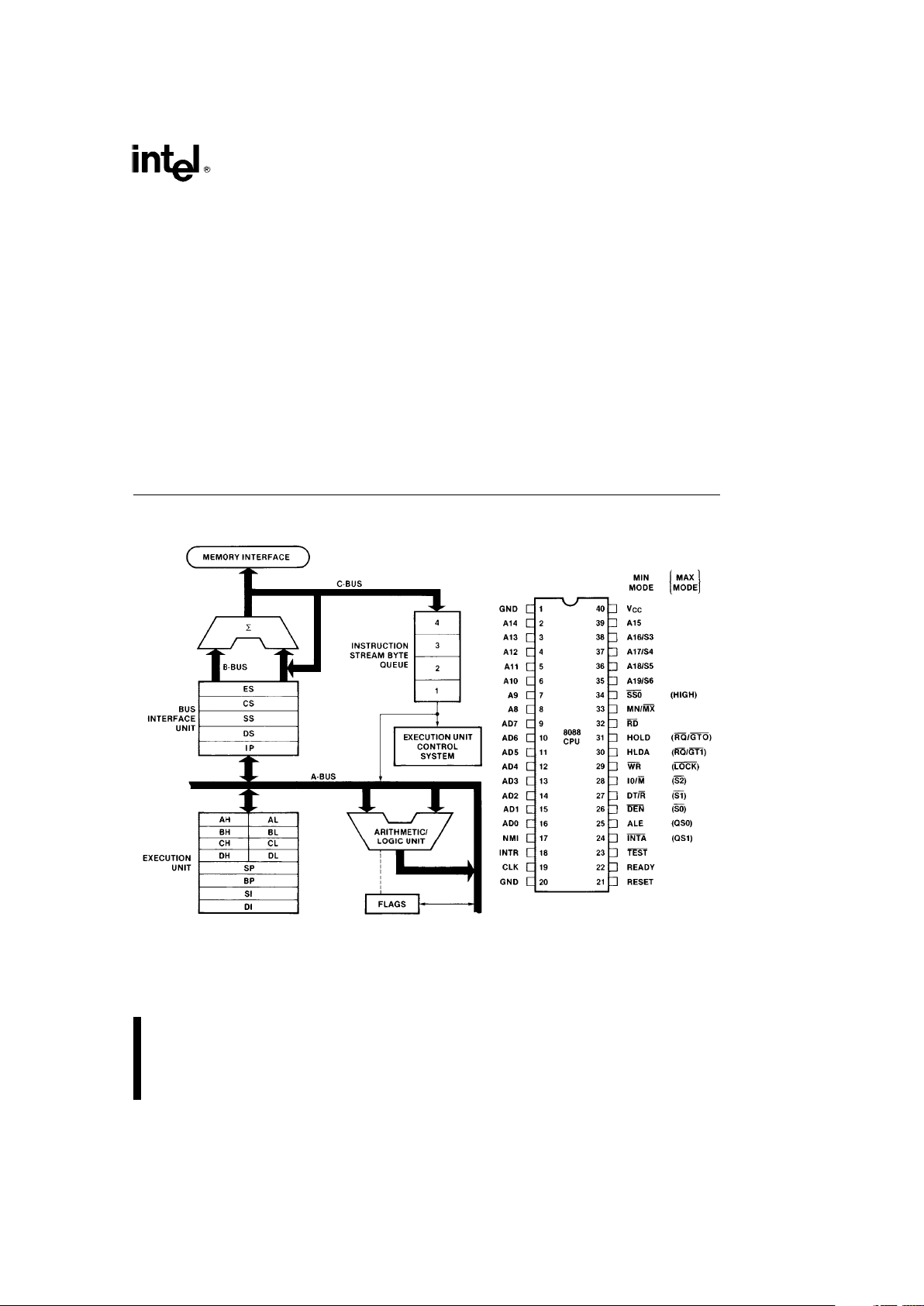
231456– 1
Figure 1. 8088 CPU Functional Block Diagram
231456– 2
Figure 2. 8088 Pin Configuration
Page 2
8088
Table 1. Pin Description
The following pin function descriptions are for 8088 systems in either minimum or maximum mode. The ‘‘local
bus’’ in these descriptions is the direct multiplexed bus interface connection to the 8088 (without regard to
additional bus buffers).
Symbol Pin No. Type Name and Function
AD7–AD0 9–16 I/O ADDRESS DATA BUS: These lines constitute the time multiplexed
memory/IO address (T1) and data (T2, T3, Tw, T4) bus. These lines are
active HIGH and float to 3-state OFF during interrupt acknowledge and
local bus ‘‘hold acknowledge’’.
A15–A8 2–8, 39 O ADDRESS BUS: These lines provide address bits 8 through 15 for the
entire bus cycle (T1 – T4). These lines do not have to be latched by ALE
to remain valid. A15 – A8 are active HIGH and float to 3-state OFF
during interrupt acknowledge and local bus ‘‘hold acknowledge’’.
A17/S4, A16/S3
A19/S6, A18/S5, 35–38 O ADDRESS/STATUS: During T1, these are the four most significant
address lines for memory operations. During I/O operations, these lines
are LOW. During memory and I/O operations, status information is
available on these lines during T2, T3, Tw, and T4. S6 is always low.
The status of the interrupt enable flag bit (S5) is updated at the
beginning of each clock cycle. S4 and S3 are encoded as shown.
This information indicates which segment register is presently being
used for data accessing.
These lines float to 3-state OFF during local bus ‘‘hold acknowledge’’.
S4 S3 Characteristics
0 (LOW) 0 Alternate Data
0 1 Stack
1 (HIGH) 0 Code or None
1 1 Data
S6 is 0 (LOW)
RD 32 O READ: Read strobe indicates that the processor is performing a
memory or I/O read cycle, depending on the state of the IO/M
pin or
S2. This signal is used to read devices which reside on the 8088 local
bus. RD
is active LOW during T2, T3 and Tw of any read cycle, and is
guaranteed to remain HIGH in T2 until the 8088 local bus has floated.
This signal floats to 3-state OFF in ‘‘hold acknowledge’’.
READY 22 I READY: is the acknowledgement from the addressed memory or I/O
device that it will complete the data transfer. The RDY signal from
memory or I/O is synchronized by the 8284 clock generator to form
READY. This signal is active HIGH. The 8088 READY input is not
synchronized. Correct operation is not guaranteed if the set up and hold
times are not met.
INTR 18 I INTERRUPT REQUEST: is a level triggered input which is sampled
during the last clock cycle of each instruction to determine if the
processor should enter into an interrupt acknowledge operation. A
subroutine is vectored to via an interrupt vector lookup table located in
system memory. It can be internally masked by software resetting the
interrupt enable bit. INTR is internally synchronized. This signal is active
HIGH.
TEST 23 I TEST: input is examined by the ‘‘wait for test’’ instruction. If the TEST
input is LOW, execution continues, otherwise the processor waits in an
‘‘idle’’ state. This input is synchronized internally during each clock
cycle on the leading edge of CLK.
2
Page 3
8088
Table 1. Pin Description (Continued)
Symbol Pin No. Type Name and Function
NMI 17 I NON-MASKABLE INTERRUPT: is an edge triggered input which causes a
type 2 interrupt. A subroutine is vectored to via an interrupt vector lookup
table located in system memory. NMI is not maskable internally by
software. A transition from a LOW to HIGH initiates the interrupt at the end
of the current instruction. This input is internally synchronized.
RESET 21 I RESET: causes the processor to immediately terminate its present activity.
The signal must be active HIGH for at least four clock cycles. It restarts
execution, as described in the instruction set description, when RESET
returns LOW. RESET is internally synchronized.
CLK 19 I CLOCK: provides the basic timing for the processor and bus controller. It is
asymmetric with a 33% duty cycle to provide optimized internal timing.
V
CC
40 VCC: is thea5Vg10% power supply pin.
GND 1, 20 GND: are the ground pins.
MN/MX 33 I MINIMUM/MAXIMUM: indicates what mode the processor is to operate in.
The two modes are discussed in the following sections.
The following pin function descriptions are for the 8088 minimum mode (i.e., MN/MXeVCC). Only the pin
functions which are unique to minimum mode are described; all other pin functions are as described above.
Symbol Pin No. Type Name and Function
IO/M 28 O STATUS LINE: is an inverted maximum mode S2 . It is used to distinguish a
memory access from an I/O access. IO/M
becomes valid in the T4 preceding a
bus cycle and remains valid until the final T4 of the cycle (I/O
e
HIGH, M
e
LOW). IO/M floats to 3-state OFF in local bus ‘‘hold acknowledge’’.
WR 29 O WRITE: strobe indicates that the processor is performing a write memory or write
I/O cycle, depending on the state of the IO/M
signal. WR is active for T2, T3, and
Tw of any write cycle. It is active LOW, and floats to 3-state OFF in local bus
‘‘hold acknowledge’’.
INTA 24 O INTA: is used as a read strobe for interrupt acknowledge cycles. It is active LOW
during T2, T3, and Tw of each interrupt acknowledge cycle.
ALE 25 O ADDRESS LATCH ENABLE: is provided by the processor to latch the address
into an address latch. It is a HIGH pulse active during clock low of T1 of any bus
cycle. Note that ALE is never floated.
DT/R 27 O DATA TRANSMIT/RECEIVE: is needed in a minimum system that desires to use
a data bus transceiver. It is used to control the direction of data flow through the
transceiver. Logically, DT/R
is equivalent to S1 in the maximum mode, and its
timing is the same as for IO/M
(TeHIGH, ReLOW). This signal floats to
3-state OFF in local ‘‘hold acknowledge’’.
DEN 26 O DATA ENABLE: is provided as an output enable for the data bus transceiver in a
minimum system which uses the transceiver. DEN
is active LOW during each
memory and I/O access, and for INTA cycles. For a read or INTA cycle, it is
active from the middle of T2 until the middle of T4, while for a write cycle, it is
active from the beginning of T2 until the middle of T4. DEN
floats to 3-state OFF
during local bus ‘‘hold acknowledge’’.
3
Page 4
8088
Table 1. Pin Description (Continued)
Symbol Pin No. Type Name and Function
HOLD,
HLDA
31, 30 I, O HOLD: indicates that another master is requesting a local bus ‘‘hold’’. To be
acknowledged, HOLD must be active HIGH. The processor receiving the ‘‘hold’’
request will issue HLDA (HIGH) as an acknowledgement, in the middle of a T4 or
Ti clock cycle. Simultaneous with the issuance of HLDA the processor will float
the local bus and control lines. After HOLD is detected as being LOW, the
processor lowers HLDA, and when the processor needs to run another cycle, it
will again drive the local bus and control lines. HOLD and HLDA have internal
pull-up resistors.
Hold is not an asynchronous input. External synchronization should be provided if
the system cannot otherwise guarantee the set up time.
SSO 34 O STATUS LINE: is logically equivalent to SO in the maximum mode. The
combination of SSO
, IO/M and DT/R allows the system to completely decode the
current bus cycle status.
IO/M DT/R SSO Characteristics
1(HIGH) 0 0 Interrupt Acknowledge
1 0 1 Read I/O Port
1 1 0 Write I/O Port
1 1 1 Halt
0(LOW) 0 0 Code Access
0 0 1 Read Memory
0 1 0 Write Memory
0 1 1 Passive
The following pin function descriptions are for the 8088/8288 system in maximum mode (i.e., MN/MX
e
GND). Only the pin functions which are unique to maximum mode are described; all other pin functions are as
described above.
Symbol Pin No. Type Name and Function
S2,S1,S0 26–28 O STATUS: is active during clock high of T4, T1, and T2, and is returned to the
passive state (1,1,1) during T3 or during Tw when READY is HIGH. This status is
used by the 8288 bus controller to generate all memory and I/O access control
signals. Any change by S2
,S1,orS0during T4 is used to indicate the beginning
of a bus cycle, and the return to the passive state in T3 and Tw is used to
indicate the end of a bus cycle.
These signals float to 3-state OFF during ‘‘hold acknowledge’’. During the first
clock cycle after RESET becomes active, these signals are active HIGH. After
this first clock, they float to 3-state OFF.
S2 S1 S0 Characteristics
0(LOW) 0 0 Interrupt Acknowledge
0 0 1 Read I/O Port
0 1 0 Write I/O Port
0 1 1 Halt
1(HIGH) 0 0 Code Access
1 0 1 Read Memory
1 1 0 Write Memory
1 1 1 Passive
4
Page 5
8088
Table 1. Pin Description (Continued)
Symbol Pin No. Type Name and Function
RQ/GT0,
RQ
/GT1
30, 31 I/O REQUEST/GRANT: pins are used by other local bus masters to force the
processor to release the local bus at the end of the processor’s current bus
cycle. Each pin is bidirectional with RQ
/GT0 having higher priority than RQ/
GT1
.RQ/GT has an internal pull-up resistor, so may be left unconnected.
The request/grant sequence is as follows (See Figure 8):
1. A pulse of one CLK wide from another local bus master indicates a local
bus request (‘‘hold’’) to the 8088 (pulse 1).
2. During a T4 or TI clock cycle, a pulse one clock wide from the 8088 to the
requesting master (pulse 2), indicates that the 8088 has allowed the local
bus to float and that it will enter the ‘‘hold acknowledge’’ state at the next
CLK. The CPU’s bus interface unit is disconnected logically from the local
bus during ‘‘hold acknowledge’’. The same rules as for HOLD/HOLDA apply
as for when the bus is released.
3. A pulse one CLK wide from the requesting master indicates to the 8088
(pulse 3) that the ‘‘hold’’ request is about to end and that the 8088 can
reclaim the local bus at the next CLK. The CPU then enters T4.
Each master-master exchange of the local bus is a sequence of three
pulses. There must be one idle CLK cycle after each bus exchange. Pulses
are active LOW.
If the request is made while the CPU is performing a memory cycle, it will
release the local bus during T4 of the cycle when all the following conditions
are met:
1. Request occurs on or before T2.
2. Current cycle is not the low bit of a word.
3. Current cycle is not the first acknowledge of an interrupt acknowledge
sequence.
4. A locked instruction is not currently executing.
If the local bus is idle when the request is made the two possible events will
follow:
1. Local bus will be released during the next clock.
2. A memory cycle will start within 3 clocks. Now the four rules for a currently
active memory cycle apply with condition number 1 already satisfied.
LOCK 29 O LOCK: indicates that other system bus masters are not to gain control of the
system bus while LOCK
is active (LOW). The LOCK signal is activated by
the ‘‘LOCK’’ prefix instruction and remains active until the completion of the
next instruction. This signal is active LOW, and floats to 3-state off in ‘‘hold
acknowledge’’.
QS1, QS0 24, 25 O QUEUE STATUS: provide status to allow external tracking of the internal
8088 instruction queue.
The queue status is valid during the CLK cycle after which the queue
operation is performed.
QS1 QS0 Characteristics
0(LOW) 0 No Operation
0 1 First Byte of Opcode from Queue
1(HIGH) 0 Empty the Queue
1 1 Subsequent Byte from Queue
Ð 34 O Pin 34 is always high in the maximum mode.
5
Page 6
8088
231456– 3
Figure 3. Memory Organization
FUNCTIONAL DESCRIPTION
Memory Organization
The processor provides a 20-bit address to memory
which locates the byte being referenced. The memory is organized as a linear array of up to 1 million
bytes, addressed as 00000(H) to FFFFF(H). The
memory is logically divided into code, data, extra
data, and stack segments of up to 64K bytes each,
with each segment falling on 16-byte boundaries
(See Figure 3).
All memory references are made relative to base addresses contained in high speed segment registers.
The segment types were chosen based on the ad-
dressing needs of programs. The segment register
to be selected is automatically chosen according to
the rules of the following table. All information in one
segment type share the same logical attributes (e.g.
code or data). By structuring memory into relocatable areas of similar characteristics and by automatically selecting segment registers, programs are
shorter, faster, and more structured.
Word (16-bit) operands can be located on even or
odd address boundaries. For address and data operands, the least significant byte of the word is stored
in the lower valued address location and the most
significant byte in the next higher address location.
The BIU will automatically execute two fetch or write
cycles for 16-bit operands.
Memory Segment
Segment Selection Rule
Reference Used Register Used
Instructions CODE (CS) Automatic with all instruction prefetch.
Stack STACK (SS) All stack pushes and pops. Memory references
relative to BP base register except data references.
Local Data DATA (DS) Data references when: relative to stack, destination
of string operation, or explicity overridden.
External (Global) Data EXTRA (ES) Destination of string operations: Explicitly selected
using a segment override.
6
Page 7
8088
Certain locations in memory are reserved for specific
CPU operations (See Figure 4). Locations from addresses FFFF0H through FFFFFH are reserved for
operations including a jump to the initial system initialization routine. Following RESET, the CPU will always begin execution at location FFFF0H where the
jump must be located. Locations 00000H through
003FFH are reserved for interrupt operations. Fourbyte pointers consisting of a 16-bit segment address
and a 16-bit offset address direct program flow to
one of the 256 possible interrupt service routines.
The pointer elements are assumed to have been
stored at their respective places in reserved memory
prior to the occurrence of interrupts.
Minimum and Maximum Modes
The requirements for supporting minimum and maximum 8088 systems are sufficiently different that
they cannot be done efficiently with 40 uniquely defined pins. Consequently, the 8088 is equipped with
a strap pin (MN/MX) which defines the system con-
231456– 4
Figure 4. Reserved Memory Locations
figuration. The definition of a certain subset of the
pins changes, dependent on the condition of the
strap pin. When the MN/MX
pin is strapped to GND,
the 8088 defines pins 24 through 31 and 34 in maximum mode. When the MN/MX
pin is strapped to
V
CC
, the 8088 generates bus control signals itself on
pins 24 through 31 and 34.
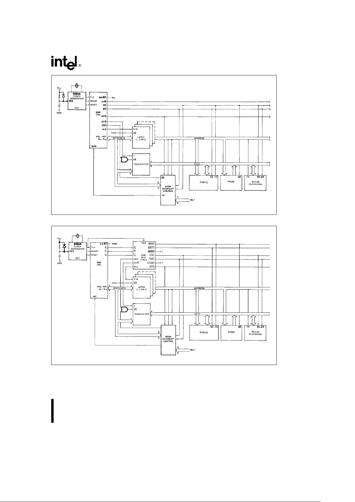
The minimum mode 8088 can be used with either a
multiplexed or demultiplexed bus. The multiplexed
bus configuration is compatible with the MCS-85
multiplexed bus peripherals. This configuration (See
Figure 5) provides the user with a minimum chip
count system. This architecture provides the 8088
processing power in a highly integrated form.
The demultiplexed mode requires one latch (for 64K
addressability) or two latches (for a full megabyte of
addressing). A third latch can be used for buffering if
the address bus loading requires it. A transceiver
can also be used if data bus buffering is required
(See Figure 6). The 8088 provides DEN
and DT/R to
control the transceiver, and ALE to latch the addresses. This configuration of the minimum mode
provides the standard demultiplexed bus structure
with heavy bus buffering and relaxed bus timing requirements.
The maximum mode employs the 8288 bus controller (See Figure 7). The 8288 decodes status lines
S0
,S1, and S2, and provides the system with all bus
control signals. Moving the bus control to the 8288
provides better source and sink current capability to
the control lines, and frees the 8088 pins for extended large system features. Hardware lock, queue
status, and two request/grant interfaces are provided by the 8088 in maximum mode. These features
allow co-processors in local bus and remote bus
configurations.
7
Page 8
8088
231456– 5
Figure 5. Multiplexed Bus Configuration
8
Page 9
8088
231456– 6
Figure 6. Demultiplexed Bus Configuration
231456– 7
Figure 7. Fully Buffered System Using Bus Controller
9
Page 10

8088
Bus Operation
The 8088 address/data bus is broken into three
partsÐthe lower eight address/data bits (AD0–
AD7), the middle eight address bits (A8– A15), and
the upper four address bits (A16 – A19). The address/data bits and the highest four address bits are
time multiplexed. This technique provides the most
efficient use of pins on the processor, permitting the
use of a standard 40 lead package. The middle eight
address bits are not multiplexed, i.e. they remain val-
id throughout each bus cycle. In addition, the bus
can be demultiplexed at the processor with a single
address latch if a standard, non-multiplexed bus is
desired for the system.
Each processor bus cycle consists of at least four
CLK cycles. These are referred to as T1, T2, T3, and
T4 (See Figure 8). The address is emitted from the
processor during T1 and data transfer occurs on the
bus during T3 and T4. T2 is used primarily for chang-
231456– 8
Figure 8. Basic System Timing
10
Page 11

8088
ing the direction of the bus during read operations. In
the event that a ‘‘NOT READY’’ indication is given
by the addressed device, ‘‘wait’’ states (Tw) are inserted between T3 and T4. Each inserted ‘‘wait’’
state is of the same duration as a CLK cycle. Periods
can occur between 8088 driven bus cycles. These
are referred to as ‘‘idle’’ states (Ti), or inactive CLK
cycles. The processor uses these cycles for internal
housekeeping.
During T1 of any bus cycle, the ALE (address latch
enable) signal is emitted (by either the processor or
the 8288 bus controller, depending on the MN/MX
strap). At the trailing edge of this pulse, a valid address and certain status information for the cycle
may be latched.
Status bits S0
,S1, and S2 are used by the bus controller, in maximum mode, to identify the type of bus
transaction according to the following table:
S2 S1 S0 Characteristics
0(LOW) 0 0 Interrupt Acknowledge
0 0 1 Read I/O
0 1 0 Write I/O
0 1 1 Halt
1(HIGH) 0 0 Instruction Fetch
1 0 1 Read Data from Memory
1 1 0 Write Data to Memory
1 1 1 Passive (No Bus Cycle)
Status bits S3 through S6 are multiplexed with high
order address bits and are therefore valid during T2
through T4. S3 and S4 indicate which segment register was used for this bus cycle in forming the address according to the following table:
S
4
S
3
Characteristics
0(LOW) 0 Alternate Data (Extra Segment)
0 1 Stack
1(HIGH) 0 Code or None
1 1 Data
S5 is a reflection of the PSW interrupt enable bit. S6
is always equal to 0.
I/O Addressing
In the 8088, I/O operations can address up to a
maximum of 64K I/O registers. The I/O address appears in the same format as the memory address on
bus lines A15– A0. The address lines A19 – A16 are
zero in I/O operations. The variable I/O instructions,
which use register DX as a pointer, have full address
capability, while the direct I/O instructions directly
address one or two of the 256 I/O byte locations in
page 0 of the I/O address space. I/O ports are addressed in the same manner as memory locations.
Designers familiar with the 8085 or upgrading an
8085 design should note that the 8085 addresses
I/O with an 8-bit address on both halves of the 16bit address bus. The 8088 uses a full 16-bit address
on its lower 16 address lines.
EXTERNAL INTERFACE
Processor Reset and Initialization
Processor initialization or start up is accomplished
with activation (HIGH) of the RESET pin. The 8088
RESET is required to be HIGH for greater than four
clock cycles. The 8088 will terminate operations on
the high-going edge of RESET and will remain dormant as long as RESET is HIGH. The low-going
transition of RESET triggers an internal reset sequence for approximately 7 clock cycles. After this
interval the 8088 operates normally, beginning with
the instruction in absolute locations FFFF0H (See
Figure 4). The RESET input is internally synchronized to the processor clock. At initialization, the HIGH
to LOW transition of RESET must occur no sooner
than 50 ms after power up, to allow complete initialization of the 8088.
NMI asserted prior to the 2nd clock after the end of
RESET will not be honored. If NMI is asserted after
that point and during the internal reset sequence,
the processor may execute one instruction before
responding to the interrupt. A hold request active
immediately after RESET will be honored before the
first instruction fetch.
All 3-state outputs float to 3-state OFF during
RESET. Status is active in the idle state for the first
clock after RESET becomes active and then floats
to 3-state OFF. ALE and HLDA are driven low.
Interrupt Operations
Interrupt operations fall into two classes: software or
hardware initiated. The software initiated interrupts
and software aspects of hardware interrupts are
specified in the instruction set description in the
iAPX 88 book or the iAPX 86,88 User’s Manual.
Hardware interrupts can be classified as nonmaskable or maskable.
11
Page 12

8088
Interrupts result in a transfer of control to a new program location. A 256 element table containing address pointers to the interrupt service program locations resides in absolute locations 0 through 3FFH
(See Figure 4), which are reserved for this purpose.
Each element in the table is 4 bytes in size and corresponds to an interrupt ‘‘type.’’ An interrupting device supplies an 8-bit type number, during the interrupt acknowledge sequence, which is used to vector
through the appropriate element to the new interrupt
service program location.
Non-Maskable Interrupt (NMI)
The processor provides a single non-maskable interrupt (NMI) pin which has higher priority than the
maskable interrupt request (INTR) pin. A typical use
would be to activate a power failure routine. The
NMI is edge-triggered on a LOW to HIGH transition.
The activation of this pin causes a type 2 interrupt.
NMI is required to have a duration in the HIGH state
of greater than two clock cycles, but is not required
to be synchronized to the clock. Any higher going
transition of NMI is latched on-chip and will be serviced at the end of the current instruction or between
whole moves (2 bytes in the case of word moves) of
a block type instruction. Worst case response to
NMI would be for multiply, divide, and variable shift
instructions. There is no specification on the occurrence of the low-going edge; it may occur before,
during, or after the servicing of NMI. Another highgoing edge triggers another response if it occurs after the start of the NMI procedure. The signal must
be free of logical spikes in general and be free of
bounces on the low-going edge to avoid triggering
extraneous responses.
Maskable Interrupt (INTR)
The 8088 provides a single interrupt request input
(INTR) which can be masked internally by software
with the resetting of the interrupt enable (IF) flag bit.
The interrupt request signal is level triggered. It is
internally synchronized during each clock cycle on
the high-going edge of CLK. To be responded to,
INTR must be present (HIGH) during the clock period preceding the end of the current instruction or the
end of a whole move for a block type instruction.
During interrupt response sequence, further interrupts are disabled. The enable bit is reset as part of
the response to any interrupt (INTR, NMI, software
interrupt, or single step), although the FLAGS register which is automatically pushed onto the stack reflects the state of the processor prior to the interrupt. Until the old FLAGS register is restored, the
enable bit will be zero unless specifically set by an
instruction.
During the response sequence (See Figure 9), the
processor executes two successive (back to back)
interrupt acknowledge cycles. The 8088 emits the
LOCK signal (maximum mode only) from T2 of the
first bus cycle until T2 of the second. A local bus
‘‘hold’’ request will not be honored until the end of
the second bus cycle. In the second bus cycle, a
byte is fetched from the external interrupt system
(e.g., 8259A PIC) which identifies the source (type)
of the interrupt. This byte is multiplied by four and
used as a pointer into the interrupt vector lookup
table. An INTR signal left HIGH will be continually
responded to within the limitations of the enable bit
and sample period. The interrupt return instruction
includes a flags pop which returns the status of the
original interrupt enable bit when it restores the
flags.
HALT
When a software HALT instruction is executed, the
processor indicates that it is entering the HALT state
in one of two ways, depending upon which mode is
strapped. In minimum mode, the processor issues
ALE, delayed by one clock cycle, to allow the system to latch the halt status. Halt status is available
on IO/M
, DT/R, and SSO. In maximum mode, the
processor issues appropriate HALT status on S2
,
S1
, and S0, and the 8288 bus controller issues one
ALE. The 8088 will not leave the HALT state when a
local bus hold is entered while in HALT. In this case,
the processor reissues the HALT indicator at the
end of the local bus hold. An interrupt request or
RESET will force the 8088 out of the HALT state.
Read/Modify/Write (Semaphore)
Operations via LOCK
The LOCK status information is provided by the
processor when consecutive bus cycles are required
during the execution of an instruction. This allows
the processor to perform read/modify/write operations on memory (via the ‘‘exchange register with
memory’’ instruction), without another system bus
master receiving intervening memory cycles. This is
useful in multiprocessor system configurations to accomplish ‘‘test and set lock’’ operations. The LOCK
signal is activated (LOW) in the clock cycle following
decoding of the LOCK prefix instruction. It is deactivated at the end of the last bus cycle of the instruction following the LOCK prefix. While LOCK
is active,
a request on a RQ
/GT pin will be recorded, and then
honored at the end of the LOCK.
12
Page 13

8088
231456– 9
Figure 9. Interrupt Acknowledge Sequence
External Synchronization via TEST
As an alternative to interrupts, the 8088 provides a
single software-testable input pin (TEST
). This input
is utilized by executing a WAIT instruction. The single WAIT instruction is repeatedly executed until the
TEST
input goes active (LOW). The execution of
WAIT does not consume bus cycles once the queue
is full.
If a local bus request occurs during WAIT execution,
the 8088 3-states all output drivers. If interrupts are
enabled, the 8088 will recognize interrupts and process them. The WAIT instruction is then refetched,
and reexecuted.
Basic System Timing
In minimum mode, the MN/MX pin is strapped to
V
CC
and the processor emits bus control signals
compatible with the 8085 bus structure. In maximum
mode, the MN/MX
pin is strapped to GND and the
processor emits coded status information which the
8288 bus controller uses to generate MULTIBUS
compatible bus control signals.
System TimingÐMinimum System
(See Figure 8)
The read cycle begins in T1 with the assertion of the
address latch enable (ALE) signal. The trailing (low
going) edge of this signal is used to latch the address information, which is valid on the address/
data bus (AD0– AD7) at this time, into the
8282/8283 latch. Address lines A8 through A15 do
not need to be latched because they remain valid
throughout the bus cycle. From T1 to T4 the IO/M
signal indicates a memory or I/O operation. At T2
the address is removed from the address/data bus
and the bus goes to a high impedance state. The
read control signal is also asserted at T2. The read
(RD) signal causes the addressed device to enable
its data bus drivers to the local bus. Some time later,
valid data will be available on the bus and the addressed device will drive the READY line HIGH.
When the processor returns the read signal to a
HIGH level, the addressed device will again 3-state
its bus drivers. If a transceiver is required to buffer
the 8088 local bus, signals DT/R
and DEN are pro-
vided by the 8088.
A write cycle also begins with the assertion of ALE
and the emission of the address. The IO/M
signal is
again asserted to indicate a memory or I/O write
operation. In T2, immediately following the address
emission, the processor emits the data to be written
into the addressed location. This data remains valid
until at least the middle of T4. During T2, T3, and
Tw, the processor asserts the write control signal.
The write (WR
) signal becomes active at the beginning of T2, as opposed to the read, which is delayed
somewhat into T2 to provide time for the bus to
float.
13
Page 14

8088
The basic difference between the interrupt acknowledge cycle and a read cycle is that the interrupt acknowledge (INTA
) signal is asserted in place of the
read (RD
) signal and the address bus is floated.
(See Figure 9) In the second of two successive INTA
cycles, a byte of information is read from the data
bus, as supplied by the interrupt system logic (i.e.
8259A priority interrupt controller). This byte identifies the source (type) of the interrupt. It is multiplied
by four and used as a pointer into the interrupt vector lookup table, as described earlier.
Bus TimingÐMedium Complexity
Systems
(See Figure 10)
For medium complexity systems, the MN/MX
pin is
connected to GND and the 8288 bus controller is
added to the system, as well as a latch for latching
the system address, and a transceiver to allow for
bus loading greater than the 8088 is capable of handling. Signals ALE, DEN
, and DT/R are generated
by the 8288 instead of the processor in this configuration, although their timing remains relatively the
same. The 8088 status outputs (S2
,S1, and S0) provide type of cycle information and become 8288 inputs. This bus cycle information specifies read
(code, data, or I/O), write (data or I/O), interrupt acknowledge, or software halt. The 8288 thus issues
control signals specifying memory read or write, I/O
read or write, or interrupt acknowledge. The 8288
provides two types of write strobes, normal and advanced, to be applied as required. The normal write
strobes have data valid at the leading edge of write.
The advanced write strobes have the same timing
as read strobes, and hence, data is not valid at the
leading edge of write. The transceiver receives the
usual T and OE
inputs from the 8288’s DT/R and
DEN
outputs.
The pointer into the interrupt vector table, which is
passed during the second INTA
cycle, can derive
from an 8259A located on either the local bus or the
system bus. If the master 8289A priority interrupt
controller is positioned on the local bus, a TTL gate
is required to disable the transceiver when reading
from the master 8259A during the interrupt acknowledge sequence and software ‘‘poll’’.
The 8088 Compared to the 8086
The 8088 CPU is an 8-bit processor designed
around the 8086 internal structure. Most internal
functions of the 8088 are identical to the equivalent
8086 functions. The 8088 handles the external bus
the same way the 8086 does with the distinction of
handling only 8 bits at a time. Sixteen-bit operands
are fetched or written in two consecutive bus cycles.
Both processors will appear identical to the software
engineer, with the exception of execution time. The
internal register structure is identical and all instructions have the same end result. The differences between the 8088 and 8086 are outlined below. The
engineer who is unfamiliar with the 8086 is referred
to the iAPX 86, 88 User’s Manual, Chapters 2 and 4,
for function description and instruction set information. Internally, there are three differences between
the 8088 and the 8086. All changes are related to
the 8-bit bus interface.
#
The queue length is 4 bytes in the 8088, whereas
the 8086 queue contains 6 bytes, or three words.
The queue was shortened to prevent overuse of
the bus by the BIU when prefetching instructions.
This was required because of the additional time
necessary to fetch instructions 8 bits at a time.
#
To further optimize the queue, the prefetching algorithm was changed. The 8088 BIU will fetch a
new instruction to load into the queue each time
there is a 1 byte hole (space available) in the
queue. The 8086 waits until a 2-byte space is
available.
#
The internal execution time of the instruction set
is affected by the 8-bit interface. All 16-bit fetches
and writes from/to memory take an additional
four clock cycles. The CPU is also limited by the
speed of instruction fetches. This latter problem
only occurs when a series of simple operations
occur. When the more sophisticated instructions
of the 8088 are being used, the queue has time to
fill and the execution proceeds as fast as the execution unit will allow.
The 8088 and 8086 are completely software compatible by virtue of their identical execution units.
Software that is system dependent may not be completely transferable, but software that is not system
dependent will operate equally as well on an 8088
and an 8086.
The hardware interface of the 8088 contains the major differences between the two CPUs. The pin assignments are nearly identical, however, with the following functional changes:
#
A8–A15ÐThese pins are only address outputs
on the 8088. These address lines are latched internally and remain valid throughout a bus cycle
in a manner similar to the 8085 upper address
lines.
#
BHE has no meaning on the 8088 and has been
eliminated.
14
Page 15

8088
#
SSO provides the SO status information in the
minimum mode. This output occurs on pin 34 in
minimum mode only. DT/R
, IO/M, and SSO pro-
vide the complete bus status in minimum mode.
#
IO/M has been inverted to be compatible with the
MCS-85 bus structure.
#
ALE is delayed by one clock cycle in the minimum mode when entering HALT, to allow the
status to be latched with ALE.
231456– 10
Figure 10. Medium Complexity System Timing
15
Page 16

8088
ABSOLUTE MAXIMUM RATINGS*
Ambient Temperature Under Bias ÀÀÀÀ0§Ctoa70§C
Case Temperature (Plastic) ААААААААА0§Ctoa95§C
Case Temperature (CERDIP) АААААААА0
§
Ctoa75§C
Storage Temperature ААААААААААb65§Ctoa150§C
Voltage on Any Pin with
Respect to Ground ААААААААААААААА
b
1.0 toa7V
Power Dissipation ААААААААААААААААААААААА2.5 Watt
NOTICE: This is a production data sheet. The specifications are subject to change without notice.
*
WARNING: Stressing the device beyond the ‘‘Absolute
Maximum Ratings’’ may cause permanent damage.
These are stress ratings only. Operation beyond the
‘‘Operating Conditions’’ is not recommended and extended exposure beyond the ‘‘Operating Conditions’’
may affect device reliability.
D.C. CHARACTERISTICS
(T
A
e
0§Cto70§C, T
CASE
(Plastic)e0§Cto95§C, T
CASE
(CERDIP)e0§Cto75§C,
T
A
e
0§Cto55§C and T
CASE
e
0§Cto75§C for P8088-2 only
T
A
is guaranteed as long as T
CASE
is not exceeded)
(V
CC
e
5Vg10% for 8088, V
CC
e
5Vg5% for 8088-2 and Extended Temperature EXPRESS)
Symbol Parameter Min Max Units Test Conditions
V
IL
Input Low Voltage
b
0.5
a
0.8 V (Note 1)
V
IH
Input High Voltage 2.0 V
CC
a
0.5 V (Notes 1, 2)
V
OL
Output Low Voltage 0.45 V I
OL
e
2.0 mA
V
OH
Output High Voltage 2.4 V I
OH
eb
400 mA
I
CC
8088 340 mA T
A
e
25§C
Power Supply Current: 8088-2 350
P8088 250
I
LI
Input Leakage Current
g
10 mA0V
s
V
IN
s
VCC(Note 3)
I
LO
Output and I/O Leakage Current
g
10 mA 0.45VsV
OUT
s
V
CC
V
CL
Clock Input Low Voltage
b
0.5
a
0.6 V
V
CH
Clock Input High Voltage 3.9 V
CC
a
1.0 V
C
IN
Capacitance If Input Buffer 15 pF fce1 MHz
(All Input Except
AD0–AD7, RQ/GT)
C
IO
Capacitance of I/O Buffer 15 pF fce1 MHz
AD
0
–AD7, RQ/GT)
NOTES:
1. V
IL
tested with MN/MX Pine0V
V
IH
tested with MN/MX Pine5V
MN/MX
Pin is a strap Pin
2. Not applicable to RQ
/GT0 and RQ/GT1 Pins (Pins 30 and 31)
3. HOLD and HLDA I
LI
Mine30 mA, Maxe500 mA
16
Page 17

8088
A.C. CHARACTERISTICS
(T
A
e
0§Cto70§C, T
CASE
(Plastic)e0§Cto95§C, T
CASE
(CERDIP)e0§Cto75§C,
T
A
e
0§Cto55§C and T
CASE
e
0§Cto80§C for P8088-2 only
T
A
is guaranteed as long as T
CASE
is not exceeded)
(V
CC
e
5Vg10% for 8088, V
CC
e
5Vg5% for 8088-2 and Extended Temperature EXPRESS)
MINIMUM COMPLEXITY SYSTEM TIMING REQUIREMENTS
Symbol Parameter
8088 8088-2
Units
Test
Min Max Min Max
Conditions
TCLCL CLK Cycle Period 200 500 125 500 ns
TCLCH CLK Low Time 118 68 ns
TCHCL CLK High Time 69 44 ns
TCH1CH2 CLK Rise Time 10 10 ns From 1.0V to 3.5V
TCL2CL2 CLK Fall Time 10 10 ns From 3.5V to 1.0V
TDVCL Data in Setup Time 30 20 ns
TCLDX Data in Hold Time 10 10 ns
TR1VCL RDY Setup Time into 8284 35 35 ns
(Notes 1, 2)
TCLR1X RDY Hold Time into 8284 0 0 ns
(Notes 1, 2)
TRYHCH READY Setup Time 118 68 ns
into 8088
TCHRYX READY Hold Time 30 20 ns
into 8088
TRYLCL READY Inactive to CLK
b
8
b
8ns
(Note 3)
THVCH HOLD Setup Time 35 20 ns
TINVCH INTR, NMI, TEST Setup Time 30 15 ns
(Note 2)
TILIH Input Rise Time (Except CLK) 20 20 ns From 0.8V to 2.0V
TIHIL Input Fall Time (Except CLK) 12 12 ns From 2.0V to 0.8V
17
Page 18

8088
A.C. CHARACTERISTICS (Continued)
TIMING RESPONSES
Symbol Parameter
8088 8088-2
Units
Test
Min Max Min Max
Conditions
TCLAV Address Valid Delay 10 110 10 60 ns
TCLAX Address Hold Time 10 10 ns
TCLAZ Address Float Delay TCLAX 80 TCLAX 50 ns
TLHLL ALE Width TCLCHb20 TCLCHb10 ns
TCLLH ALE Active Delay 80 50 ns
TCHLL ALE Inactive Delay 85 55 ns
TLLAX Address Hold Time to TCHCLb10 TCHCLb10 ns
ALE Inactive
TCLDV Data Valid Delay 10 110 10 60 ns
TCHDX Data Hold Time 10 10 ns
TWHDX Data Hold Time after WR TCLCHb30 TCLCHb30 ns
TCVCTV Control Active Delay 1 10 110 10 70 ns
TCHCTV Control Active Delay 2 10 110 10 60 ns
TCVCTX Control Inactive Delay 10 110 10 70 ns
TAZRL Address Float to READ 0 0 ns
Active
TCLRL RD Active Delay 10 165 10 100 ns
TCLRH RD Inactive Delay 10 150 10 80 ns
TRHAV RD Inactive to Next TCLCLb45 TCLCLb40 ns
Address Active
TCLHAV HLDA Valid Delay 10 160 10 100 ns
TRLRH RD Width 2TCLCLb75 2TCLCLb50 ns
TWLWH WR Width 2TCLCLb60 2TCLCLb40 ns
TAVAL Address Valid to ALE Low TCLCHb60 TCLCHb40 ns
TOLOH Output Rise Time 20 20 ns From 0.8V to 2.0V
TOHOL Output Fall Time 12 12 ns From 2.0V to 0.8V
NOTES:
1. Signal at 8284A shown for reference only. See 8284A data sheet for the most recent specifications.
2. Set up requirement for asynchronous signal only to guarantee recognition at next CLK.
3. Applies only to T2 state (8 ns into T3 state).
18
Page 19

8088
A.C. TESTING INPUT, OUTPUT WAVEFORM
231456– 11
A.C. Testing; Inputs are driven at 2.4V for a logic ‘‘1’’ and 0.45V
for a logic ‘‘0’’. Timing measurements are made at 1.5V for both a
logic ‘‘1’’ and logic ‘‘0’’.
A.C. TESTING LOAD CIRCUIT
231456– 12
C
L
Includes Jig Capacitance
WAVEFORMS
BUS TIMINGÐMINIMUM MODE SYSTEM
231456– 13
19
Page 20

8088
WAVEFORMS (Continued)
BUS TIMINGÐMINIMUM MODE SYSTEM (Continued)
231456– 14
NOTES:
1. All signals switch between V
OH
and VOLunless otherwise specified.
2. RDY is sampled near the end of T
2,T3,Tw
to determine if Twmachines states are to be inserted.
3. Two INTA cycles run back-to-back. The 8088 local ADDR/DATA bus is floating during both INTA cycles. Control
signals are shown for the second INTA cycle.
4. Signals at 8284 are shown for reference only.
5. All timing measurements are made at 1.5V unless otherwise noted.
20
Page 21

8088
A.C. CHARACTERISTICS
MAX MODE SYSTEM (USING 8288 BUS CONTROLLER)
TIMING REQUIREMENTS
Symbol Parameter
8088 8088-2
Units
Test
Min Max Min Max
Conditions
TCLCL CLK Cycle Period 200 500 125 500 ns
TCLCH CLK Low Time 118 68 ns
TCHCL CLK High Time 69 44 ns
TCH1CH2 CLK Rise Time 10 10 ns From 1.0V to 3.5V
TCL2CL1 CLK Fall Time 10 10 ns From 3.5V to 1.0V
TDVCL Data in Setup Time 30 20 ns
TCLDX Data in Hold Time 10 10 ns
TR1VCL RDY Setup Time into 8284 35 35 ns
(Notes 1, 2)
TCLR1X RDY Hold Time into 8284 0 0 ns
(Notes 1, 2)
TRYHCH READY Setup Time into 8088 118 68 ns
TCHRYX READY Hold Time into 8088 30 20 ns
TRYLCL READY Inactive to CLK
b
8
b
8ns
(Note 4)
TINVCH Setup Time for Recognition 30 15 ns
(INTR, NMI, TEST) (Note 2)
TGVCH RQ/GT Setup Time 30 15 ns
TCHGX RQ Hold Time into 8088 40 30 ns
TILIH Input Rise Time (Except CLK) 20 20 ns From 0.8V to 2.0V
TIHIL Input Fall Time (Except CLK) 12 12 ns From 2.0V to 0.8V
21
Page 22

8088
A.C. CHARACTERISTICS (Continued)
TIMING RESPONSES
Symbol Parameter
8088 8088-2
Units
Test
Min Max Min Max
Conditions
TCLML Command Active Delay 10 35 10 35 ns
(Note 1)
TCLMH Command Inactive Delay 10 35 10 35 ns
(Note 1)
TRYHSH READY Active to 110 65 ns
Status Passive (Note 3)
TCHSV Status Active Delay 10 110 10 60 ns
TCLSH Status Inactive Delay 10 130 10 70 ns
TCLAV Address Valid Delay 10 110 10 60 ns
TCLAX Address Hold Time 10 10 ns
TCLAZ Address Float Delay TCLAX 80 TCLAX 50 ns
TSVLH Status Valid to ALE High 15 15 ns
(Note 1)
TSVMCH Status Valid to MCE High 15 15 ns
(Note 1)
TCLLH CLK Low to ALE Valid 15 15 ns
(Note 1)
TCLMCH CLK Low to MCE (Note 1) 15 15 ns
TCHLL ALE Inactive Delay (Note 1) 15 15 ns
TCLMCL MCE Inactive Delay (Note 1) 15 15 ns
TCLDV Data Valid Delay 10 110 10 60 ns
TCHDX Data Hold Time 10 10 ns
C
L
e
20–100 pF for
TCVNV Control Active Delay 5 45 5 45 ns
All 8088 Outputs
(Note 1)
in Addition to
TCVNX Control Inactive Delay 10 45 10 45 ns
Internal Loads
(Note 1)
TAZRL Address Float to 0 0 ns
Read Active
TCLRL RD Active Delay 10 165 10 100 ns
TCLRH RD Inactive Delay 10 150 10 80 ns
TRHAV RD Inactive to Next TCLCLb45 TCLCLb40 ns
Address Active
TCHDTL Direction Control 50 50 ns
Active Delay (Note 1)
TCHDTH Direction Control 30 30 ns
Inactive Delay (Note 1)
TCLGL GT Active Delay 85 50 ns
TCLGH GT Inactive Delay 85 50 ns
TRLRH RD Width 2TCLCLb75 2TCLCLb50 ns
TOLOH Output Rise Time 20 20 ns From 0.8V to 2.0V
TOHOL Output Fall Time 12 12 ns From 2.0V to 0.8V
NOTES:
1. Signal at 8284 or 8288 shown for reference only.
2. Setup requirement for asynchronous signal only to guarantee recognition at next CLK.
3. Applies only to T3 and wait states.
4. Applies only to T2 state (8 ns into T3 state).
22
Page 23

8088
A.C. TESTING INPUT, OUTPUT WAVEFORM
231456– 11
A.C. Testing; Inputs are driven at 2.4V for a logic ‘‘1’’ and 0.45V
for a logic ‘‘0’’. Timing measurements are made at 1.5V for both a
logic ‘‘1’’ and logic ‘‘0’’.
A.C. TESTING LOAD CIRCUIT
231456– 12
C
L
Includes Jig Capacitance
WAVEFORMS (Continued)
BUS TIMINGÐMAXIMUM MODE SYSTEM
231456– 15
23
Page 24

8088
WAVEFORMS (Continued)
BUS TIMINGÐMAXIMUM MODE SYSTEM (USING 8288)
NOTES: 231456– 16
1. All signals switch between VOHand VOLunless otherwise specified.
2. RDY is sampled near the end of T
2,T3,Tw
to determine if Twmachines states are to be inserted.
3. Cascade address is valid between first and second INTA cycles.
4. Two INTA cycles run back-to-back. The 8088 local ADDR/DATA bus is floating during both INTA cycles. Control for
pointer address is shown for second INTA cycle.
5. Signals at 8284 or 8288 are shown for reference only.
6. The issuance of the 8288 command and control signals (MRDC
, MWTC, AMWC, IORC, IOWC, AIOWC, INTA and
DEN) lags the active high 8288 CEN.
7. All timing measurements are made at 1.5V unless otherwise noted.
8. Status inactive in state just prior to T4.
24
Page 25

8088
WAVEFORMS (Continued)
ASYNCHRONOUS SIGNAL RECOGNITION
NOTE: 231456– 17
1. Setup requirements for asynchronous signals only to
guarantee recognition at next CLK.
BUS LOCK SIGNAL TIMING
(MAXIMUM MODE ONLY)
231456– 18
REQUEST/GRANT SEQUENCE TIMING (MAXIMUM MODE ONLY)
NOTE: 231456– 19
1. The coprocessor may not drive the busses outside the region shown without risking contention.
HOLD/HOLD ACKNOWLEDGE TIMING (MINIMUM MODE ONLY)
231456– 20
25
Page 26

8088
8086/8088 Instruction Set Summary
Mnemonic and
Instruction Code
Description
DATA TRANSFER
MOV
e
Move: 76543210 76543210 76543210 76543210
Register/Memory to/from Register 100010dw mod reg r/m
Immediate to Register/Memory 1100011w mod000r/m data data if we1
Immediate to Register 1011wreg data data if we1
Memory to Accumulator 1010000w addr-low addr-high
Accumulator to Memory 1010001w addr-low addr-high
Register/Memory to Segment Register 10001110 mod0regr/m
Segment Register to Register/Memory 10001100 mod0regr/m
PUSHePush:
Register/Memory 11111111 mod110r/m
Register 01010reg
Segment Register 000reg110
POPePop:
Register/Memory 10001111 mod000r/m
Register 01011reg
Segment Register 000reg111
XCHGeExchange:
Register/Memory with Register 1000011w modregr/m
Register with Accumulator 10010reg
INeInput from:
Fixed Port 1110010w port
Variable Port 1110110w
OUTeOutput to:
Fixed Port 1110011w port
Variable Port 1110111w
XLATeTranslate Byte to AL 11010111
LEAeLoad EA to Register 10001101 modregr/m
LDSeLoad Pointer to DS 11000101 modregr/m
LESeLoad Pointer to ES 11000100 modregr/m
LAHFeLoad AH with Flags 10011111
SAHFeStore AH into Flags 10011110
PUSHFePush Flags 10011100
POPFePop Flags 10011101
26
Page 27

8088
8086/8088 Instruction Set Summary (Continued)
Mnemonic and
Instruction Code
Description
ARITHMETIC 76543210 76543210 76543210 76543210
ADD
e
Add:
Reg./Memory with Register to Either 000000dw modregr/m
Immediate to Register/Memory 100000sw mod000r/m data data if s:we01
Immediate to Accumulator 0000010w data data if we1
ADCeAdd with Carry:
Reg./Memory with Register to Either 000100dw modregr/m
Immediate to Register/Memory 100000sw mod010r/m data data if s:we01
Immediate to Accumulator 0001010w data data if we1
INCeIncrement:
Register/Memory 1111111w mod000r/m
Register 01000reg
AAAeASCII Adjust for Add 00110111
BAAeDecimal Adjust for Add 00100111
SUBeSubtract:
Reg./Memory and Register to Either 001010dw modregr/m
Immediate from Register/Memory 100000sw mod101r/m data data if s:we01
Immediate from Accumulator 0010110w data data if we1
SSBeSubtract with Borrow
Reg./Memory and Register to Either 000110dw modregr/m
Immediate from Register/Memory 100000sw mod011r/m data data if s:we01
Immediate from Accumulator 000111w data data if we1
DECeDecrement:
Register/memory 1111111w mod001r/m
Register 01001 reg
NEGeChange sign 1111011w mod011 r/m
CMPeCompare:
Register/Memory and Register 001110dw modregr/m
Immediate with Register/Memory 100000sw mod111r/m data data if s:we01
Immediate with Accumulator 0011110w data data if we1
AASeASCII Adjust for Subtract 00111111
DASeDecimal Adjust for Subtract 00101111
MULeMultiply (Unsigned) 1111011w mod100r/m
IMULeInteger Multiply (Signed) 1111011w mod101r/m
AAMeASCII Adjust for Multiply 11010100 00001010
DIVeDivide (Unsigned) 1111011w mod110r/m
IDIVeInteger Divide (Signed) 1111011w mod111r/m
AADeASCII Adjust for Divide 11010101 00001010
CBWeConvert Byte to Word 10011000
CWDeConvert Word to Double Word 10011001
27
Page 28

8088
8086/8088 Instruction Set Summary (Continued)
Mnemonic and
Instruction Code
Description
LOGIC 76543210 76543210 76543210 76543210
NOTeInvert 1111011w mod010r/m
SHL/SALeShift Logical/Arithmetic Left 110100vw mod100r/m
SHReShift Logical Right 110100vw mod101r/m
SAReShift Arithmetic Right 110100vw mod111r/m
ROLeRotate Left 110100vw mod000r/m
ROReRotate Right 110100vw mod001r/m
RCLeRotate Through Carry Flag Left 110100vw mod010r/m
RCReRotate Through Carry Right 110100vw mod011r/m
ANDeAnd:
Reg./Memory and Register to Either 001000dw modregr/m
Immediate to Register/Memory 1000000w mod100r/m data data if we1
Immediate to Accumulator 0010010w data data if we1
TESTeAnd Function to Flags. No Result:
Register/Memory and Register 1000010w modregr/m
Immediate Data and Register/Memory 1111011w mod000r/m data data if we1
Immediate Data and Accumulator 1010100w data data if we1
OReOr:
Reg./Memory and Register to Either 000010dw modregr/m
Immediate to Register/Memory 1000000w mod001r/m data data if we1
Immediate to Accumulator 0000110w data data if we1
XOReExclusive or:
Reg./Memory and Register to Either 001100dw modregr/m
Immediate to Register/Memory 1000000w mod110r/m data data if we1
Immediate to Accumulator 0011010w data data if we1
STRING MANIPULATION
REPeRepeat 1111001z
MOVSeMove Byte/Word 1010010w
CMPSeCompare Byte/Word 1010011w
SCASeScan Byte/Word 1010111w
LODSeLoad Byte/Wd to AL/AX 1010110w
STOSeStor Byte/Wd from AL/A 1010101w
CONTROL TRANSFER
CALL
e
Call:
Direct Within Segment 11101000 disp-low disp-high
Indirect Within Segment 11111111 mod010r/m
Direct Intersegment 10011010 offset-low offset-high
seg-low seg-high
Indirect Intersegment 11111111 mod011r/m
28
Page 29

8088
8086/8088 Instruction Set Summary (Continued)
Mnemonic and
Instruction Code
Description
JMPeUnconditional Jump: 76543210 76543210 76543210
Direct Within Segment 11101001 disp-low disp-high
Direct Within Segment-Short 11101011 disp
Indirect Within Segment 11111111 mod100r/m
Direct Intersegment 11101010 offset-low offset-high
seg-low seg-high
Indirect Intersegment 11111111 mod101r/m
RETeReturn from CALL:
Within Segment 11000011
Within Seg Adding Immed to SP 11000010 data-low data-high
Intersegment 11001011
Intersegment Adding Immediate to SP 11001010 data-low data-high
JE/JZeJump on Equal/Zero 01110100 disp
JL/JNGEeJump on Less/Not Greater
01111100 disp
or Equal
JLE/JNGeJump on Less or Equal/
01111110 disp
Not Greater
JB/JNAEeJump on Below/Not Above
01110010 disp
or Equal
JBE/JNAeJump on Below or Equal/
01110110 disp
Not Above
JP/JPEeJump on Parity/Parity Even 01111010 disp
JOeJump on Overflow 01110000 disp
JSeJump on Sign 01111000 disp
JNE/JNZeJump on Not Equal/Not Zero 01110101 disp
JNL/JGEeJump on Not Less/Greater
01111101 disp
or Equal
JNLE/JGeJump on Not Less or Equal/
01111111 disp
Greater
JNB/JAEeJump on Not Below/Above
01110011 disp
or Equal
JNBE/JAeJump on Not Below or
01110111 disp
Equal/Above
JNP/JPOeJump on Not Par/Par Odd 01111011 disp
JNOeJump on Not Overflow 01110001 disp
JNSeJump on Not Sign 01111001 disp
LOOPeLoop CX Times 11100010 disp
LOOPZ/LOOPEeLoop While Zero/Equal 11100001 disp
LOOPNZ/LOOPNEeLoop While Not
11100000 disp
Zero/Equal
JCXZeJump on CX Zero 11100011 disp
INTeInterrupt
Type Specified 11001101 type
Type 3 11001100
INTOeInterrupt on Overflow 11001110
IRETeInterrupt Return 11001111
29
Page 30

8088
8086/8088 Instruction Set Summary (Continued)
Mnemonic and
Instruction Code
Description
76543210 76543210
PROCESSOR CONTROL
CLCeClear Carry 11111000
CMCeComplement Carry 11110101
STCeSet Carry 11111001
CLDeClear Direction 11111100
STDeSet Direction 11111101
CLIeClear Interrupt 11111010
STIeSet Interrupt 11111011
HLTeHalt 11110100
WAITeWait 10011011
ESCeEscape (to External Device) 11011xxx modxxxr/m
LOCKeBus Lock Prefix 11110000
NOTES:
AL
e
8-bit accumulator
AX
e
16-bit accumulator
CX
e
Count register
DS
e
Data segment
ES
e
Extra segment
Above/below refers to unsigned value
Greater
e
more positive:
Less
e
less positive (more negative) signed values
if d
e
1 then ‘‘to’’ reg; if de0 then ‘‘from’’ reg
if w
e
1 then word instruction; if we0 then byte
instruction
if mod
e
11 then r/m is treated as a REG field
if mod
e
00 then DISPe0*, disp-low and disp-high are
absent
if mod
e
01 then DISPedisp-low sign-extended to
16 bits, disp-high is absent
if mod
e
10 then DISPedisp-high; disp-low
if r/m
e
000 then EAe(BX)a(SI)aDISP
if r/m
e
001 then EAe(BX)a(DI)aDISP
if r/m
e
010 then EAe(BP)a(SI)aDISP
if r/m
e
011 then EAe(BP)a(DI)aDISP
if r/m
e
100 then EAe(SI)aDISP
if r/m
e
101 then EAe(DI)aDISP
if r/m
e
110 then EAe(BP)aDISP*
if r/m
e
111 then EAe(BX)aDISP
DISP follows 2nd byte of instruction (before data if required)
*except if mod
e
00 and r/methen EAedisp-high:
disp-low.
if s:w
e
01 then 16 bits of immediate data form the oper-
and
if s:w
e
11 then an immediate data byte is sign extended
to form the 16-bit operand
if v
e
0 then ‘‘count’’e1; if ve1 then ‘‘count’’ in (CL)
register
x
e
don’t care
z is used for string primitives for comparison with ZF FLAG
SEGMENT OVERRIDE PREFIX
001reg110
REG is assigned according to the following table:
16-Bit (we1) 8-Bit (we0) Segment
000 AX 000 AL 00 ES
001 CX 001 CL 01 CS
010 DX 010 DL 10 SS
011 BX 011 BL 11 DS
100 SP 100 AH
101 BP 101 CH
110 SI 110 DH
111 DI 111 BH
Instructions which reference the flag register file as a 16-bit
object use the symbol FLAGS to represent the file:
FLAGS
e
X:X:X:X:(OF):(DF):(IF):(TF):(SF):(ZF):X:(AF):X:(PF):X:(CF)
Mnemonics
©
Intel, 1978
DATA SHEET REVISION REVIEW
The following list represents key differences between this and the -005 data sheet. Please review
this summary carefully.
1. The Intel 8088 implementation technology
(HMOS) has been changed to (HMOS-II).
30
 Loading...