

Page 1
User’s Manual
78K0/KC2
8-bit Single-Chip Microcontrollers
μ
PD78F0511
μ
PD78F0511(A)
μ
PD78F0511(A2)
μ
PD78F0512
μ
PD78F0513
μ
PD78F0514
μ
PD78F0515
μ
PD78F0513D
μ
PD78F0515D
The μPD78F0513D and 78F0515D have on-chip debug functions.
Do not use these products for mass production because its reliability cannot be guaranteed after the on-chip debug
function has been used, due to issues with respect to the number of times the flash memory can be rewritten. NEC
Electronics does not accept complaints concerning these products.
Document No. U17336EJ5V0UD00 (5th edition)
Date Published February 2007 N CP(K)
μ
PD78F0512(A)
μ
PD78F0513(A)
μ
PD78F0514(A)
μ
PD78F0515(A)
μ
PD78F0512(A2)
μ
PD78F0513(A2)
μ
PD78F0514(A2)
μ
PD78F0515(A2)
Printed in Japan
2005
Page 2

[MEMO]
2
User’s Manual U17336EJ5V0UD
Page 3
1
VOLTAGE APPLICATION WAVEFORM AT INPUT PIN
Waveform distortion due to input noise or a reflected wave may cause malfunction. If the input of the
CMOS device stays in the area between V
IL
2
3
4
User’s Manual U17336EJ5V0UD
3
Page 4

EEPROM is a trademark of NEC Electronics Corporation.
Windows and Windows NT are registered trademarks or trademarks of Microsoft Corporation in the United
States and/or other countries.
PC/AT is a trademark of International Business Machines Corporation.
HP9000 series 700 and HP-UX are trademarks of Hewlett-Packard Company.
SPARCstation is a trademark of SPARC International, Inc.
Solaris and SunOS are trademarks of Sun Microsystems, Inc.
SuperFlash is a registered trademark of Silicon Storage Technology, Inc. in several countries including the
United States and Japan.
4
User’s Manual U17336EJ5V0UD
Page 5

®
Caution: This product uses SuperFlash
technology licensed from Silicon Storage Technology, Inc.
The information in this document is current as of December, 2006. The information is subject to
change without notice. For actual design-in, refer
User’s Manual U17336EJ5V0UD
5
Page 6
INTRODUCTION
Readers This manual is intended for user engineers who wish to understand the functions of the
78K0/KC2 and design and develop application systems and programs for these devices.
The target products are as follows.
78K0/KC2:
<R>
<R>
Purpose This manual is intended to give users an understanding of the functions described in the
Organization below.
Organization The 78K0/KC2 manual is separated into two parts: this manual and the instructions
edition (common to 78K0 microcontrollers).
μ
PD78F0511, 78F0512, 78F0513, 78F0514, 78F0515, 78F0513D,
78F0515D, 78F0511(A), 78F0512(A), 78F0513(A), 78F0514(A),
78F0515(A), 78F0511(A2), 78F0512(A2), 78F0513(A2), 78F0514(A2),
78F0515(A2)
78K0/KC2
User’s Manual
(This Manual)
• Pin functions
• Internal block functions
• Interrupts
• Other on-chip peripheral functions
• Electrical specifications
How to Read This Manual It is assumed that the readers of this manual have general knowledge of electrical
engineering, logic circuits, and microcontrollers.
<R>
• When using this manual as the manual for (A) grade products and (A2) grade
products:
→ Only the quality grade differs between standard products, (A) grade products, and
(A2) grade products. Read the part number as follows.
•
μ
PD78F0511→ μPD78F0511(A), 78F0511(A2)
•
μ
PD78F0512→ μPD78F0512(A), 78F0512(A2)
•
μ
PD78F0513→ μPD78F0513(A), 78F0513(A2)
•
μ
PD78F0514→ μPD78F0514(A), 78F0514(A2)
•
μ
PD78F0515→ μPD78F0515(A), 78F0515(A2)
• To gain a general understanding of functions:
→ Read this manual in the order of the CONTENTS. The mark “<R>” shows major
revised points. The revised points can be easily searched by copying an “<R>” in
the PDF file and specifying it in the “Find what:” field.
• How to interpret the register format:
→ For a bit number enclosed in angle brackets, the bit name is defined as a
reserved word in the RA78K0, and is defined as an sfr variable using the
#pragma sfr directive in the CC78K0.
78K/0 Series
User’s Manual
Instructions
• CPU functions
• Instruction set
• Explanation of each instruction
6
User’s Manual U17336EJ5V0UD
Page 7
• To check the details of a register when you know the register name:
→ See APPENDIX C REGISTER INDEX.
• To know details of the 78K0 microcontroller instructions:
→ Refer to the separate document 78K/0 Series Instructions User’s Manual
(U12326E).
Conventions Data significance: Higher digits on the left and lower digits on the right
Active low representations: ××× (overscore over pin and signal name)
Note: Footnote for item marked with Note in the text
Caution: Information requiring particular attention
Remark: Supplementary information
Numerical representations: Binary
Decimal
Hexadecimal
...
×××× or ××××B
...
××××
...
××××H
Related Documents The related documents indicated in this publication may include preliminary versions.
However, preliminary versions are not marked as such.
Documents Related to Devices
<R>
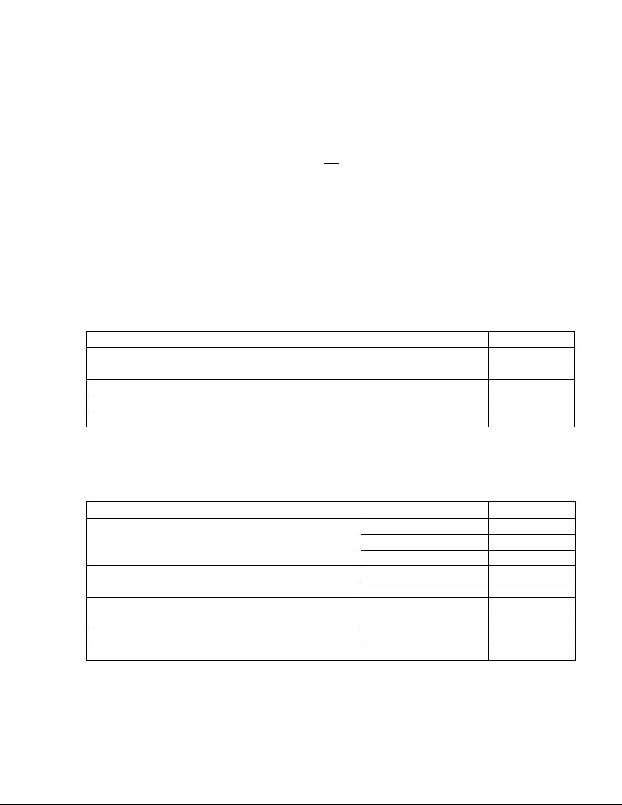
Document Name Document No.
78K0/KC2 User’s Manual This manual
78K/0 Series Instructions User’s Manual U12326E
78K0/Kx2 Flash Memory Programming (Programmer) Application Note U17739E
78K0/Kx2 Flash Memory Self Programming User’s Manual
78K0/Kx2 EEPROMTM Emulation Application Note
Note
Note
U17516E
U17517E
Note This document is under engineering management. For details, consult an NEC Electronics sales
representative.
Documents Related to Development Tools (Software) (User’s Manuals)
Document Name Document No.
RA78K0 Ver. 3.80 Assembler Package
ID78K0-QB Ver. 2.90 Integrated Debugger Operation U17437E
PM plus Ver. 5.20 U16934E
Operation U17199E
Language U17198E
Structured Assembly Language U17197E
Operation U17201E CC78K0 Ver. 3.70 C Compiler
Language U17200E
Operation U17246E SM+ System Simulator
User Open Interface U17247E
Caution The related documents listed above are subject to change without notice. Be sure to use the latest
version of each document when designing.
User’s Manual U17336EJ5V0UD
7
Page 8
Documents Related to Development Tools (Hardware) (User’s Manuals)
Document Name Document No.
QB-78K0KX2 In-Circuit Emulator U17341E
QB-78K0MINI On-Chip Debug Emulator U17029E
<R>
QB-MINI2 On-Chip Debug Emulator with Programming Function U18371E
Documents Related to Flash Memory Programming (User’s Manuals)
Document Name Document No.
PG-FP4 Flash Memory Programmer U15260E
PG-FPL3 Flash Memory Programmer U17454E
Other Documents
Document Name Document No.
SEMICONDUCTOR SELECTION GUIDE − Products and Packages − X13769X
Semiconductor Device Mount Manual Note
Quality Grades on NEC Semiconductor Devices C11531E
NEC Semiconductor Device Reliability/Quality Control System C10983E
Guide to Prevent Damage for Semiconductor Devices by Electrostatic Discharge (ESD) C11892E
Note See the “Semiconductor Device Mount Manual” website (http://www.necel.com/pkg/en/mount/index.html).
Caution The related documents listed above are subject to change without notice. Be sure to use the latest
version of each document when designing.
8
User’s Manual U17336EJ5V0UD
Page 9

CONTENTS
CHAPTER 1 OUTLINE ............................................................................................................................ 17
1.1 Features .................................................................................................................................... 17
1.2 Applications ............................................................................................................................. 18
1.3 Ordering Information ............................................................................................................... 19
1.4 Pin Configuration (Top View).................................................................................................. 20
1.5 78K0/Kx2 Microcontroller Lineup........................................................................................... 26
1.6 Block Diagram.......................................................................................................................... 29
1.7 Outline of Functions ................................................................................................................ 30
CHAPTER 2 PIN FUNCTIONS ............................................................................................................... 33
2.1 Pin Function List...................................................................................................................... 33
2.2 Description of Pin Functions.................................................................................................. 36
2.2.1 P00 and P01 (port 0).................................................................................................................. 36
2.2.2 P10 to P17 (port 1).....................................................................................................................37
2.2.3 P20 to P27 (port 2).....................................................................................................................38
2.2.4 P30 to P33 (port 3).....................................................................................................................38
2.2.5 P40 and P41 (port 4) (44-pin and 48-pin products only) ............................................................39
2.2.6 P60 to P63 (port 6).....................................................................................................................39
2.2.7 P70 to P75 (port 7).....................................................................................................................40
2.2.8 P120 to P124 (port 12)...............................................................................................................40
2.2.9 P130 (port 13) (48-pin products only).........................................................................................41
2.2.10 P140 (port 14) (48-pin products only).........................................................................................41
2.2.11 AVREF ........................................................................................................................................42
2.2.12 AVSS ..........................................................................................................................................42
2.2.13 RESET.......................................................................................................................................42
2.2.14 REGC.........................................................................................................................................42
2.2.15 VDD ............................................................................................................................................42
2.2.16 VSS ............................................................................................................................................42
2.2.17 FLMD0 ....................................................................................................................................... 42
2.3 Pin I/O Circuits and Recommended Connection of Unused Pins....................................... 43
CHAPTER 3 CPU ARCHITECTURE ...................................................................................................... 47
3.1 Memory Space.......................................................................................................................... 47
3.1.1 Internal program memory space ................................................................................................56
3.1.2 Internal data memory space.......................................................................................................58
3.1.3 Special function register (SFR) area ..........................................................................................59
3.1.4 Data memory addressing ...........................................................................................................59
3.2 Processor Registers ................................................................................................................ 65
3.2.1 Control registers.........................................................................................................................65
3.2.2 General-purpose registers .........................................................................................................69
3.2.3 Special function registers (SFRs)...............................................................................................70
3.3 Instruction Address Addressing ............................................................................................ 75
3.3.1 Relative addressing....................................................................................................................75
User’s Manual U17336EJ5V0UD
9
Page 10

3.3.2 Immediate addressing ............................................................................................................... 76
3.3.3 Table indirect addressing .......................................................................................................... 77
3.3.4 Register addressing .................................................................................................................. 77
3.4 Operand Address Addressing ................................................................................................ 78
3.4.1 Implied addressing .................................................................................................................... 78
3.4.2 Register addressing .................................................................................................................. 79
3.4.3 Direct addressing ...................................................................................................................... 80
3.4.4 Short direct addressing ............................................................................................................. 81
3.4.5 Special function register (SFR) addressing ............................................................................... 82
3.4.6 Register indirect addressing...................................................................................................... 83
3.4.7 Based addressing...................................................................................................................... 84
3.4.8 Based indexed addressing ........................................................................................................ 85
3.4.9 Stack addressing....................................................................................................................... 86
CHAPTER 4 PORT FUNCTIONS ........................................................................................................... 87
4.1 Port Functions.......................................................................................................................... 87
4.2 Port Configuration ................................................................................................................... 89
4.2.1 Port 0......................................................................................................................................... 90
4.2.2 Port 1......................................................................................................................................... 92
4.2.3 Port 2......................................................................................................................................... 97
4.2.4 Port 3......................................................................................................................................... 99
4.2.5 Port 4 (44-pin and 48-pin products only) ..................................................................................102
4.2.6 Port 6........................................................................................................................................103
4.2.7 Port 7........................................................................................................................................105
4.2.8 Port 12......................................................................................................................................106
4.2.9 Port 13 (48-pin products only) ..................................................................................................109
4.2.10 Port 14 (48-pin products only)..................................................................................................110
4.3 Registers Controlling Port Function .................................................................................... 111
4.4 Port Function Operations...................................................................................................... 116
4.4.1 Writing to I/O port .....................................................................................................................116
4.4.2 Reading from I/O port...............................................................................................................116
4.4.3 Operations on I/O port..............................................................................................................116
4.5 Settings of Port Mode Register and Output Latch When Using Alternate Function....... 117
4.6 Cautions on 1-bit Manipulation Instruction for Port Register n (Pn) ................................ 119
CHAPTER 5 CLOCK GENERATOR .................................................................................................... 120
5.1 Functions of Clock Generator............................................................................................... 120
5.2 Configuration of Clock Generator ........................................................................................ 121
5.3 Registers Controlling Clock Generator ............................................................................... 123
5.4 System Clock Oscillator ........................................................................................................ 132
5.4.1 X1 oscillator..............................................................................................................................132
5.4.2 XT1 oscillator ...........................................................................................................................132
5.4.3 When subsystem clock is not used ..........................................................................................135
5.4.4 Internal high-speed oscillator ...................................................................................................135
5.4.5 Internal low-speed oscillator.....................................................................................................135
5.4.6 Prescaler ..................................................................................................................................135
5.5 Clock Generator Operation ................................................................................................... 136
5.6 Controlling Clock ................................................................................................................... 140
10
User’s Manual U17336EJ5V0UD
Page 11

5.6.1 Controlling high-speed system clock........................................................................................140
5.6.2 Example of controlling internal high-speed oscillation clock..................................................... 143
5.6.3 Example of controlling subsystem clock...................................................................................145
5.6.4 Example of controlling internal low-speed oscillation clock ......................................................147
5.6.5 Clocks supplied to CPU and peripheral hardware.................................................................... 147
5.6.6 CPU clock status transition diagram ........................................................................................148
5.6.7 Condition before changing CPU clock and processing after changing CPU clock ...................153
5.6.8 Time required for switchover of CPU clock and main system clock .........................................154
5.6.9 Conditions before clock oscillation is stopped..........................................................................155
5.6.10 Peripheral hardware and source clocks ...................................................................................156
CHAPTER 6 16-BIT TIMER/EVENT COUNTER 00........................................................................... 157
6.1 Functions of 16-bit Timer/Event Counter 00 ....................................................................... 157
6.2 Configuration of 16-bit Timer/Event Counter 00................................................................. 158
6.3 Registers Controlling 16-bit Timer/Event Counter 00 ........................................................ 163
6.4 Operation of 16-bit Timer/Event Counter 00 ....................................................................... 171
6.4.1 Interval timer operation ............................................................................................................171
6.4.2 Square wave output operation .................................................................................................174
6.4.3 External event counter operation .............................................................................................177
6.4.4 Operation in clear & start mode entered by TI000 pin valid edge input.................................... 180
6.4.5 Free-running timer operation....................................................................................................193
6.4.6 PPG output operation...............................................................................................................202
6.4.7 One-shot pulse output operation..............................................................................................205
6.4.8 Pulse width measurement operation........................................................................................210
6.5 Special Use of TM00 .............................................................................................................. 218
6.5.1 Rewriting CR010 during TM00 operation .................................................................................218
6.5.2 Setting LVS00 and LVR00 .......................................................................................................218
6.6 Cautions for 16-bit Timer/Event Counter 00........................................................................ 220
CHAPTER 7 8-BIT TIMER/EVENT COUNTERS 50 AND 51 .......................................................... 224
7.1 Functions of 8-bit Timer/Event Counters 50 and 51........................................................... 224
7.2 Configuration of 8-bit Timer/Event Counters 50 and 51 .................................................... 224
7.3 Registers Controlling 8-bit Timer/Event Counters 50 and 51............................................ 227
7.4 Operations of 8-bit Timer/Event Counters 50 and 51......................................................... 232
7.4.1 Operation as interval timer ....................................................................................................... 232
7.4.2 Operation as external event counter ........................................................................................234
7.4.3 Square-wave output operation .................................................................................................235
7.4.4 PWM output operation .............................................................................................................236
7.5 Cautions for 8-bit Timer/Event Counters 50 and 51 ........................................................... 240
CHAPTER 8 8-BIT TIMERS H0 AND H1 .......................................................................................... 241
8.1 Functions of 8-bit Timers H0 and H1 ................................................................................... 241
8.2 Configuration of 8-bit Timers H0 and H1............................................................................. 241
8.3 Registers Controlling 8-bit Timers H0 and H1 .................................................................... 245
8.4 Operation of 8-bit Timers H0 and H1 ................................................................................... 251
8.4.1 Operation as interval timer/square-wave output.......................................................................251
8.4.2 Operation as PWM output........................................................................................................254
User’s Manual U17336EJ5V0UD
11
Page 12

8.4.3 Carrier generator operation (8-bit timer H1 only)......................................................................260
CHAPTER 9 WATCH TIMER................................................................................................................ 267
9.1 Functions of Watch Timer ..................................................................................................... 267
9.2 Configuration of Watch Timer............................................................................................... 268
9.3 Register Controlling Watch Timer........................................................................................ 269
9.4 Watch Timer Operations........................................................................................................ 271
9.4.1 Watch timer operation ..............................................................................................................271
9.4.2 Interval timer operation.............................................................................................................271
9.5 Cautions for Watch Timer ..................................................................................................... 272
CHAPTER 10 WATCHDOG TIMER ..................................................................................................... 273
10.1 Functions of Watchdog Timer .............................................................................................. 273
10.2 Configuration of Watchdog Timer........................................................................................ 274
10.3 Register Controlling Watchdog Timer ................................................................................. 275
10.4 Operation of Watchdog Timer............................................................................................... 276
10.4.1 Controlling operation of watchdog timer ...................................................................................276
10.4.2 Setting overflow time of watchdog timer...................................................................................277
10.4.3 Setting window open period of watchdog timer ........................................................................278
CHAPTER 11 CLOCK OUTPUT CONTROLLER (48-PIN PRODUCTS ONLY) .............................. 280
11.1 Functions of Clock Output Controller.................................................................................. 280
11.2 Configuration of Clock Output Controller ........................................................................... 281
11.3 Registers Controlling Clock Output Controller................................................................... 281
11.4 Operations of Clock Output Controller................................................................................ 283
CHAPTER 12 A/D CONVERTER ......................................................................................................... 284
12.1 Function of A/D Converter .................................................................................................... 284
12.2 Configuration of A/D Converter............................................................................................ 285
12.3 Registers Used in A/D Converter.......................................................................................... 287
12.4 A/D Converter Operations ..................................................................................................... 295
12.4.1 Basic operations of A/D converter............................................................................................295
12.4.2 Input voltage and conversion results ........................................................................................297
12.4.3 A/D converter operation mode .................................................................................................298
12.5 How to Read A/D Converter Characteristics Table............................................................. 300
12.6 Cautions for A/D Converter................................................................................................... 302
CHAPTER 13 SERIAL INTERFACE UART0 ...................................................................................... 306
13.1 Functions of Serial Interface UART0.................................................................................... 306
13.2 Configuration of Serial Interface UART0 ............................................................................. 307
13.3 Registers Controlling Serial Interface UART0..................................................................... 310
13.4 Operation of Serial Interface UART0.................................................................................... 315
13.4.1 Operation stop mode................................................................................................................315
13.4.2 Asynchronous serial interface (UART) mode ...........................................................................316
13.4.3 Dedicated baud rate generator.................................................................................................322
13.4.4 Calculation of baud rate ...........................................................................................................323
12
User’s Manual U17336EJ5V0UD
Page 13

CHAPTER 14 SERIAL INTERFACE UART6 ...................................................................................... 327
14.1 Functions of Serial Interface UART6 ................................................................................... 327
14.2 Configuration of Serial Interface UART6............................................................................. 331
14.3 Registers Controlling Serial Interface UART6 .................................................................... 334
14.4 Operation of Serial Interface UART6.................................................................................... 343
14.4.1 Operation stop mode................................................................................................................343
14.4.2 Asynchronous serial interface (UART) mode ........................................................................... 344
14.4.3 Dedicated baud rate generator ................................................................................................357
14.4.4 Calculation of baud rate ...........................................................................................................359
CHAPTER 15 SERIAL INTERFACE CSI10 ........................................................................................ 364
15.1 Functions of Serial Interface CSI10 ..................................................................................... 364
15.2 Configuration of Serial Interface CSI10............................................................................... 365
15.3 Registers Controlling Serial Interface CSI10 ...................................................................... 367
15.4 Operation of Serial Interface CSI10...................................................................................... 371
15.4.1 Operation stop mode................................................................................................................371
15.4.2 3-wire serial I/O mode..............................................................................................................371
CHAPTER 16 SERIAL INTERFACE IIC0 ........................................................................................... 382
16.1 Functions of Serial Interface IIC0......................................................................................... 382
16.2 Configuration of Serial Interface IIC0 .................................................................................. 385
16.3 Registers to Control Serial Interface IIC0............................................................................ 388
16.4 I2C Bus Mode Functions ........................................................................................................ 401
16.4.1 Pin configuration ......................................................................................................................401
16.5 I2C Bus Definitions and Control Methods............................................................................ 402
16.5.1 Start conditions ........................................................................................................................402
16.5.2 Addresses ................................................................................................................................ 403
16.5.3 Transfer direction specification ................................................................................................403
16.5.4 ACK..........................................................................................................................................404
16.5.5 Stop condition ..........................................................................................................................405
16.5.6 Wait..........................................................................................................................................406
16.5.7 Canceling wait..........................................................................................................................408
16.5.8 Interrupt request (INTIIC0) generation timing and wait control.................................................408
16.5.9 Address match detection method.............................................................................................409
16.5.10 Error detection .........................................................................................................................409
16.5.11 Extension code ........................................................................................................................410
16.5.12 Arbitration.................................................................................................................................411
16.5.13 Wakeup function ......................................................................................................................412
16.5.14 Communication reservation .....................................................................................................413
16.5.15 Cautions...................................................................................................................................416
16.5.16 Communication operations ......................................................................................................417
16.5.17 Timing of I2C interrupt request (INTIIC0) occurrence ...............................................................425
16.6 Timing Charts ......................................................................................................................... 446
CHAPTER 17 MULTIPLIER/DIVIDER (μPD78F0514, 78F0515, AND 78F0515D ONLY)............... 453
17.1 Functions of Multiplier/Divider............................................................................................. 453
17.2 Configuration of Multiplier/Divider....................................................................................... 453
User’s Manual U17336EJ5V0UD
13
Page 14

17.3 Register Controlling Multiplier/Divider ................................................................................ 457
17.4 Operations of Multiplier/Divider............................................................................................ 458
17.4.1 Multiplication operation.............................................................................................................458
17.4.2 Division operation.....................................................................................................................460
CHAPTER 18 INTERRUPT FUNCTIONS ............................................................................................ 462
18.1 Interrupt Function Types....................................................................................................... 462
18.2 Interrupt Sources and Configuration................................................................................... 462
18.3 Registers Controlling Interrupt Functions .......................................................................... 466
18.4 Interrupt Servicing Operations ............................................................................................. 474
18.4.1 Maskable interrupt acknowledgment........................................................................................474
18.4.2 Software interrupt request acknowledgment ............................................................................476
18.4.3 Multiple interrupt servicing........................................................................................................477
18.4.4 Interrupt request hold ...............................................................................................................480
CHAPTER 19 KEY INTERRUPT FUNCTION ..................................................................................... 481
19.1 Functions of Key Interrupt .................................................................................................... 481
19.2 Configuration of Key Interrupt.............................................................................................. 481
19.3 Register Controlling Key Interrupt ....................................................................................... 482
CHAPTER 20 STANDBY FUNCTION .................................................................................................. 483
20.1 Standby Function and Configuration................................................................................... 483
20.1.1 Standby function.......................................................................................................................483
20.1.2 Registers controlling standby function......................................................................................483
20.2 Standby Function Operation................................................................................................. 486
20.2.1 HALT mode ..............................................................................................................................486
20.2.2 STOP mode .............................................................................................................................491
CHAPTER 21 RESET FUNCTION........................................................................................................ 497
21.1 Register for Confirming Reset Source................................................................................. 505
CHAPTER 22 POWER-ON-CLEAR CIRCUIT...................................................................................... 506
22.1 Functions of Power-on-Clear Circuit ................................................................................... 506
22.2 Configuration of Power-on-Clear Circuit............................................................................. 507
22.3 Operation of Power-on-Clear Circuit.................................................................................... 507
22.4 Cautions for Power-on-Clear Circuit.................................................................................... 510
CHAPTER 23 LOW-VOLTAGE DETECTOR ....................................................................................... 512
23.1 Functions of Low-Voltage Detector...................................................................................... 512
23.2 Configuration of Low-Voltage Detector............................................................................... 513
23.3 Registers Controlling Low-Voltage Detector ...................................................................... 513
23.4 Operation of Low-Voltage Detector...................................................................................... 516
23.4.1 When used as reset .................................................................................................................517
23.4.2 When used as interrupt ............................................................................................................522
23.5 Cautions for Low-Voltage Detector...................................................................................... 527
14
User’s Manual U17336EJ5V0UD
Page 15

CHAPTER 24 OPTION BYTE............................................................................................................... 530
24.1 Functions of Option Bytes.................................................................................................... 530
24.2 Format of Option Byte........................................................................................................... 532
CHAPTER 25 FLASH MEMORY.......................................................................................................... 535
25.1 Internal Memory Size Switching Register ........................................................................... 535
25.2 Internal Expansion RAM Size Switching Register.............................................................. 536
25.3 Writing with Flash Memory Programmer............................................................................. 537
25.4 Programming Environment................................................................................................... 545
25.5 Communication Mode ........................................................................................................... 545
25.6 Handling of Pins on Board.................................................................................................... 547
25.6.1 FLMD0 pin ...............................................................................................................................547
25.6.2 Serial interface pins..................................................................................................................547
25.6.3 RESET pin ...............................................................................................................................549
25.6.4 Port pins...................................................................................................................................549
25.6.5 REGC pin.................................................................................................................................549
25.6.6 Other signal pins ......................................................................................................................549
25.6.7 Power supply ...........................................................................................................................550
25.7 Programming Method ............................................................................................................ 551
25.7.1 Controlling flash memory .........................................................................................................551
25.7.2 Flash memory programming mode ..........................................................................................551
25.7.3 Selecting communication mode ...............................................................................................552
25.7.4 Communication commands......................................................................................................553
25.8 Security Settings.................................................................................................................... 554
25.9 Processing Time for Each Command When PG-FP4 Is Used (Reference) ...................... 556
25.10 Flash Memory Programming by Self Programming ........................................................... 557
25.10.1 Boot swap function...................................................................................................................564
CHAPTER 26 ON-CHIP DEBUG FUNCTION (μPD78F0513D AND 78F0515D ONLY)................... 566
26.1 Connecting QB-78K0MINI or QB-MINI2 to μPD78F0513D and 78F0515D......................... 566
26.2 Reserved Area Used by QB-78K0MINI and QB-MINI2 ........................................................ 568
CHAPTER 27 INSTRUCTION SET ...................................................................................................... 569
27.1 Conventions Used in Operation List.................................................................................... 569
27.1.1 Operand identifiers and specification methods ........................................................................569
27.1.2 Description of operation column...............................................................................................570
27.1.3 Description of flag operation column ........................................................................................570
27.2 Operation List......................................................................................................................... 571
27.3 Instructions Listed by Addressing Type ............................................................................. 579
CHAPTER 28 ELECTRICAL SPECIFICATIONS (STANDARD PRODUCTS)................................... 582
CHAPTER 29 ELECTRICAL SPECIFICATIONS ((A) GRADE PRODUCTS) .................................... 603
CHAPTER 30 ELECTRICAL SPECIFICATIONS ((A2) GRADE PRODUCTS:
T
A = −40 to +110°C)........................................................................................................ 622
User’s Manual U17336EJ5V0UD
15
Page 16

CHAPTER 31 ELECTRICAL SPECIFICATIONS ((A2) GRADE PRODUCTS:
TA = −40 to +125°C)........................................................................................................ 641
CHAPTER 32 PACKAGE DRAWINGS ................................................................................................ 660
CHAPTER 33 RECOMMENDED SOLDERING CONDITIONS ........................................................... 665
CHAPTER 34 CAUTIONS FOR WAIT................................................................................................. 666
34.1 Cautions for Wait.................................................................................................................... 666
34.2 Peripheral Hardware That Generates Wait .......................................................................... 667
APPENDIX A DEVELOPMENT TOOLS............................................................................................... 668
A.1 Software Package .................................................................................................................. 672
A.2 Language Processing Software............................................................................................ 672
A.3 Control Software .................................................................................................................... 673
A.4 Flash Memory Writing Tools ................................................................................................. 674
A.4.1 When using flash memory programmer PG-FP4, FL-PR4, PG-FPL3, and FP-LITE3 ..............674
A.4.2 When using on-chip debug emulator with programming function QB-MINI2 ............................674
A.5 Debugging Tools (Hardware) ................................................................................................ 675
A.5.1 When using in-circuit emulator QB-78K0KX2...........................................................................675
A.5.2 When using on-chip debug emulator QB-78K0MINI.................................................................676
A.5.3 When using on-chip debug emulator with programming function QB-MINI2 ............................676
A.6 Debugging Tools (Software) ................................................................................................. 677
APPENDIX B NOTES ON TARGET SYSTEM DESIGN ................................................................... 678
APPENDIX C REGISTER INDEX ......................................................................................................... 680
C.1 Register Index (In Alphabetical Order with Respect to Register Names) ........................ 680
C.2 Register Index (In Alphabetical Order with Respect to Register Symbol) ....................... 683
APPENDIX D LIST OF CAUTIONS ..................................................................................................... 687
APPENDIX E REVISION HISTORY....................................................................................................... 713
E.1 Major Revisions in This Edition............................................................................................ 713
E.2 Revision History of Preceding Editions............................................................................... 719
16
User’s Manual U17336EJ5V0UD
Page 17
CHAPTER 1 OUTLINE
1.1 Features
{ Minimum instruction execution time can be changed from high speed (0.1 μs: @ 20 MHz operation with high-
speed system clock) to ultra low-speed (122
{ General-purpose register: 8 bits × 32 registers (8 bits × 8 registers × 4 banks)
{ ROM, RAM capacities
μ
s: @ 32.768 kHz operation with subsystem clock)
<R>
Program Memory
Part Number
μ
PD78F0511 16 KB 768 bytes
μ
PD78F0512 24 KB
μ
PD78F0513, 78F0513D 32 KB
μ
PD78F0514 48 KB 1 KB
μ
PD78F0515, 78F0515D
Flash memory
(ROM)
Note
Internal High-Speed RAM
1 KB
60 KB
Data Memory Item
Note
Internal Expansion RAM
2 KB
−
Note The internal flash memory, internal high-speed RAM capacities, and internal expansion RAM capacities
can be changed using the internal memory size switching register (IMS) and the internal expansion RAM
size switching register (IXS). For IMS and IXS, see 25.1 Memory Size Switching Register and 25.2
Internal Expansion RAM Size Switching Register.
{ On-chip single-power-supply flash memory
{ Self-programming (with boot swap function)
{ On-chip debug function (
μ
PD78F0513D and 78F0515D only)
Note
{ On-chip power-on-clear (POC) circuit and low-voltage detector (LVI)
{ On-chip watchdog timer (operable with the on-chip internal low-speed oscillation clock)
{ On-chip multiplier/divider (16 bits × 16 bits, 32 bits / 16 bits)
(
μ
PD78F0514, 78F0515, and 78F0515D only)
{ On-chip key interrupt function
{ On-chip clock output controller
{ I/O ports:
38-pin products: 31 (N-ch open drain: 4)
44-pin products: 37 (N-ch open drain: 4)
48-pin products: 41 (N-ch open drain: 4)
Note The
μ
PD78F0513D and 78F0515D have on-chip debug functions. Do not use these products for mass
production because its reliability cannot be guaranteed after the on-chip debug function has been used, due
to issues with respect to the number of times the flash memory can be rewritten. NEC Electronics does not
accept complaints concerning these products.
Note
User’s Manual U17336EJ5V0UD
17
Page 18

CHAPTER 1 OUTLINE
{ Timer: 7 channels
• 16-bit timer/event counter: 1 channel
• 8-bit timer/event counter: 2 channels
• 8-bit timer: 2 channels
• Watch timer: 1 channel
• Watchdog timer: 1 channel
{ Serial interface: 3 channels
• UART (LIN (Local Interconnect Network)-bus supported: 1 channel
• CSI/UART
2
• I
C: 1 channel
{ 10-bit resolution A/D converter (AV
Note
: 1 channel
REF = 2.3 to 5.5 V): 8 channels (38-pin products: 6 channels)
{ Power supply voltage
• Standard products, (A) grade products: V
• (A2) grade products: V
DD = 1.8 to 5.5 V
DD = 2.7 to 5.5 V
{ Operating ambient temperature
• Standard products, (A) grade products: T
• (A2) grade products: T
A = –40 to +85°C
A = –40 to +110°C, TA = –40 to +125°C
Note Select either of the functions of these alternate-function pins.
1.2 Applications
18
User’s Manual U17336EJ5V0UD
Page 19

<R>
<R>
<R>
<R>
<R>
<R>
<R>
<R>
<R>
<R>
<R>
<R>
CHAPTER 1 OUTLINE
1.3 Ordering Information
• Flash memory version
Part Number Package Quality Grade
μ
PD78F0511GA-8EU-A
μ
PD78F0511GB-UES-A
μ
PD78F0511MC-GAA-AX
μ
PD78F0512GA-8EU-A
μ
PD78F0512GB-UES-A
μ
PD78F0512MC-GAA-AX
μ
PD78F0513GA-8EU-A
μ
PD78F0513GB-UES-A
μ
PD78F0513MC-GAA-AX
μ
PD78F0514GA-8EU-A
μ
PD78F0515GA-8EU-A
μ
PD78F0513DGB-UES-A
μ
PD78F0513DMC-GAA-AX
μ
PD78F0515DGA-8EU-A
μ
PD78F0511GA(A)-GAM-AX
μ
PD78F0511GB(A)-GAF-AX
μ
PD78F0512GA(A)-GAM-AX
μ
PD78F0512GB(A)-GAF-AX
μ
PD78F0513GA(A)-GAM-AX
μ
PD78F0513GB(A)-GAF-AX
μ
PD78F0514GA(A)-GAM-AX
μ
PD78F0515GA(A)-GAM-AX
μ
PD78F0511GA(A2)-GAM-AX
μ
PD78F0511GB(A2)-GAF-AX
μ
PD78F0512GA(A2)-GAM-AX
μ
PD78F0512GB(A2)-GAF-AX
μ
PD78F0513GA(A2)-GAM-AX
μ
PD78F0513GB(A2)-GAF-AX
μ
PD78F0514GA(A2)-GAM-AX
μ
PD78F0515GA(A2)-GAM-AX
Note 1
Note 1
Note 1
Note 2
Note 2
Notes 1, 2
Notes 1. Under development
2. The
μ
PD78F0513D and 78F0515D have on-chip debug functions. Do not use these products for mass
production because its reliability cannot be guaranteed after the on-chip debug function has been used,
due to issues with respect to the number of times the flash memory can be rewritten. NEC Electronics
does not accept complaints concerning these products.
Remark Products with -A and -AX at the end of the part number are lead-free products.
Please refer to "Quality Grades on NEC Semiconductor Devices" (Document No. C11531E) published by
NEC Electronics Corporation to know the specification of the quality grade on the device and its
recommended applications.
48-pin plastic LQFP (fine pitch) (7 x 7) Standard
44-pin plastic LQFP (10 x 10) Standard
38-pin plastic SSOP (7.62 mm (300))
48-pin plastic LQFP (fine pitch) (7 x 7) Standard
44-pin plastic LQFP (10 x 10) Standard
38-pin plastic SSOP (7.62 mm (300))
48-pin plastic LQFP (fine pitch) (7 x 7) Standard
44-pin plastic LQFP (10 x 10) Standard
38-pin plastic SSOP (7.62 mm (300))
48-pin plastic LQFP (fine pitch) (7 x 7) Standard
48-pin plastic LQFP (fine pitch) (7 x 7) Standard
44-pin plastic LQFP (10 x 10) Standard
38-pin plastic SSOP (7.62 mm (300)) Standard
48-pin plastic LQFP (fine pitch) (7 x 7)
48-pin plastic LQFP (fine pitch) (7 x 7) Special
44-pin plastic LQFP (10 x 10) Special
48-pin plastic LQFP (fine pitch) (7 x 7) Special
44-pin plastic LQFP (10 x 10) Special
48-pin plastic LQFP (fine pitch) (7 x 7) Special
44-pin plastic LQFP (10 x 10) Special
48-pin plastic LQFP (fine pitch) (7 x 7) Special
48-pin plastic LQFP (fine pitch) (7 x 7) Special
48-pin plastic LQFP (fine pitch) (7 x 7) Special
44-pin plastic LQFP (10 x 10) Special
48-pin plastic LQFP (fine pitch) (7 x 7) Special
44-pin plastic LQFP (10 x 10) Special
48-pin plastic LQFP (fine pitch) (7 x 7) Special
44-pin plastic LQFP (10 x 10) Special
48-pin plastic LQFP (fine pitch) (7 x 7) Special
48-pin plastic LQFP (fine pitch) (7 x 7) Special
Standard
Standard
Standard
Standard
User’s Manual U17336EJ5V0UD
19
Page 20
1.4 Pin Configuration (Top View)
<R>
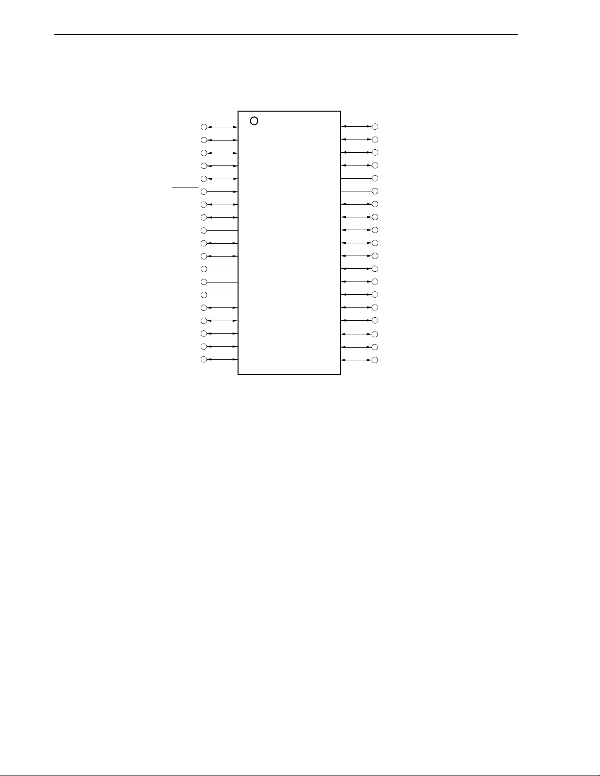
• 38-pin plastic SSOP (7.62 mm (300))
CHAPTER 1 OUTLINE
ANI1/P21
ANI0/P20
P01/TI010/TO00
P00/TI000
P120/INTP0/EXLVI
RESET
P124/XT2/EXCLKS
P123/XT1
FLMD0
P122/X2/EXCLK/OCD0B
P121/X1/OCD0A
Note
Note
REGC
V
SS
V
DD
P60/SCL0
P61/SDA0
P62/EXSCL0
P63
P33/TI51/TO51/INTP4
1
2
3
4
5
6
7
8
9
10
11
12
13
14
15
16
17
18
19
38
37
36
35
34
33
32
31
30
29
28
27
26
25
24
23
22
21
20
ANI2/P22
ANI3/P23
ANI4/P24
ANI5/P25
AV
SS
AV
REF
P10/SCK10/TxD0
P11/SI10/RxD0
P12/SO10
P13/TxD6
P14/RxD6
P15/TOH0
P16/TOH1/INTP5
P17/TI50/TO50
P30/INTP1
P31/INTP2/OCD1A
P32/INTP3/OCD1B
P70/KR0
P71/KR1
Note
μ
PD78F0513D (product with on-chip debug function) only
Cautions 1. Make AV
2. Connect the REGC pin to V
SS the same potential as VSS.
SS via a capacitor (0.47 to 1
μ
F: recommended).
3. ANI0/P20 to ANI5/P25 are set in the analog input mode after release of reset.
Note
Note
20
User’s Manual U17336EJ5V0UD
Page 21

CHAPTER 1 OUTLINE
Pin Identification
ANI0 to ANI5: Analog input P70, P71: Port 7
AV
REF: Analog reference voltage P120 to P124: Port 12
AV
SS: Analog ground REGC: Regulator capacitance
EXCLK: External clock input RESET: Reset
(main system clock) RxD0, RxD6: Receive data
EXCLKS: External clock input SCK10, SCL0: Serial clock input/output
(subsystem clock) SDA0: Serial data input/output
EXLVI: External potential input SI10: Serial data input
for low-voltage detector SO10: Serial data output
EXSCL0: External serial clock input TI000, TI010,
FLMD0: Flash programming mode TI50, TI51: Timer input
INTP0 to INTP5: External interrupt input TO00,
KR0, KR1: Key return TO50, TO51,
OCD0A
OCD1A
Note
, OCD0B
Note
, OCD1B
Note
, TOH0, TOH1: Timer output
Note
: On-chip debug input/output TxD0, TxD6: Transmit data
P00, P01: Port 0 V
DD: Power supply
P10 to P17: Port 1 VSS: Ground
P20 to P25: Port 2 X1, X2: Crystal oscillator (main system
P30 to P33: Port 3 clock)
P60 to P63: Port 6 XT1, XT2: Crystal oscillator (subsystem clock)
Note
μ
PD78F0513D (product with on-chip debug function) only
User’s Manual U17336EJ5V0UD
21
Page 22
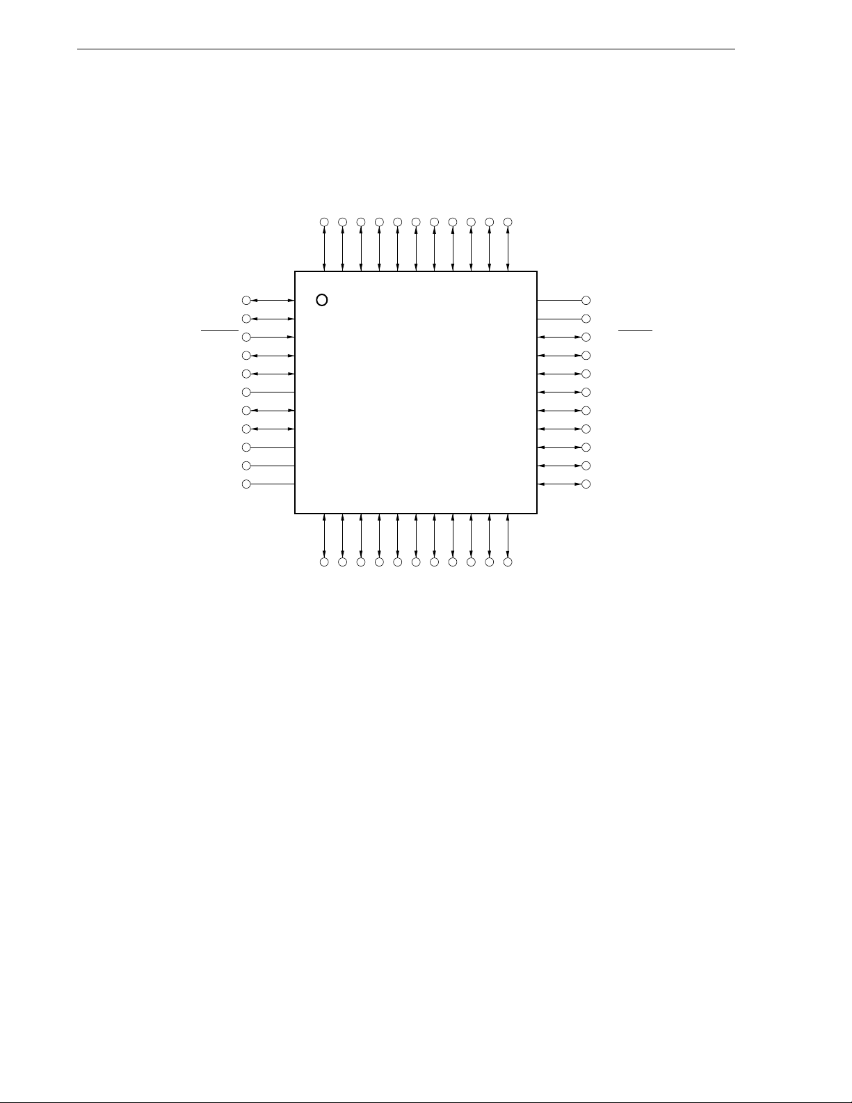
• 44-pin plastic LQFP (10 × 10)
P41
P40
RESET
P124/XT2/EXCLKS
P123/XT1
FLMD0
P122/X2/EXCLK/OCD0B
P121/X1/OCD0A
Note
Note
REGC
V
V
SS
DD
CHAPTER 1 OUTLINE
P120/INTP0/EXLVI
P00/TI000
P01/TI010/TO00
ANI0/P20
ANI1/P21
ANI2/P22
ANI3/P23
ANI4/P24
44 43 42 41 40 39 38 37 36 35 34
1
2
3
4
5
6
7
8
9
10
11
12 13 14 15 16 17 18 19 20 21 22
ANI5/P25
ANI6/P26
ANI7/P27
33
32
31
30
29
28
27
26
25
24
23
AV
SS
AV
REF
P10/SCK10/TxD0
P11/SI10/RxD0
P12/SO10
P13/TxD6
P14/RxD6
P15/TOH0
P16/TOH1/INTP5
P17/TI50/TO50
P30/INTP1
Note
Note
P70/KR0
P60/SCL0
P61/SDA0
P63
P73/KR3
P72/KR2
P71/KR1
P62/EXSCL0
P32/INTP3/OCD1B
P33/TI51/TO51/INTP4
P31/INTP2/OCD1A
Note μPD78F0513D (product with on-chip debug function) only
Cautions 1. Make AV
2. Connect the REGC pin to V
SS the same potential as VSS.
SS via a capacitor (0.47 to 1
μ
F: recommended).
3. ANI0/P20 to ANI7/P27 are set in the analog input mode after release of reset.
22
User’s Manual U17336EJ5V0UD
Page 23

CHAPTER 1 OUTLINE
Pin Identification
ANI0 to ANI7: Analog input P70 to P73: Port 7
AV
REF: Analog reference voltage P120 to P124: Port 12
AV
SS: Analog ground REGC: Regulator capacitance
EXCLK: External clock input RESET: Reset
(main system clock) RxD0, RxD6: Receive data
EXCLKS: External clock input SCK10, SCL0: Serial clock input/output
(subsystem clock) SDA0: Serial data input/output
EXLVI: External potential input SI10: Serial data input
for low-voltage detector SO10: Serial data output
EXSCL0: External serial clock input TI000, TI010,
FLMD0: Flash programming mode TI50, TI51: Timer input
INTP0 to INTP5: External interrupt input TO00,
KR0 to KR3: Key return TO50, TO51,
OCD0A
OCD1A
Note
, OCD0B
Note
, OCD1B
Note
, TOH0, TOH1: Timer output
Note
: On-chip debug input/output TxD0, TxD6: Transmit data
P00, P01: Port 0 V
DD: Power supply
P10 to P17: Port 1 VSS: Ground
P20 to P27: Port 2 X1, X2: Crystal oscillator (main system clock)
P30 to P33: Port 3 XT1, XT2: Crystal oscillator (subsystem clock)
P40, P41: Port 4
P60 to P63: Port 6
Note
μ
PD78F0513D (product with on-chip debug function) only
User’s Manual U17336EJ5V0UD
23
Page 24
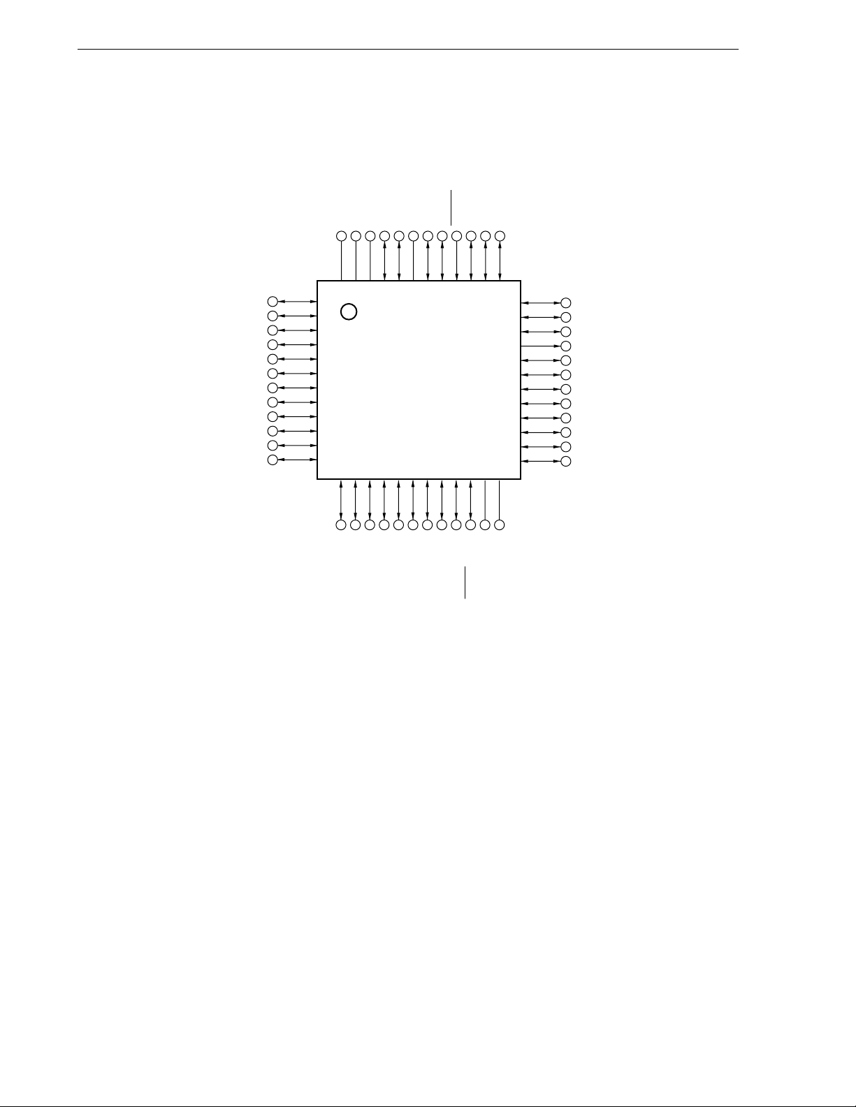
• 48-pin plastic LQFP (fine pitch) (7 × 7)
CHAPTER 1 OUTLINE
Note
Note
P60/SCL0
P61/SDA0
P62/EXSCL0
P63
P33/TI51/TO51/INTP4
P75
P74
P73/KR3
P72/KR2
P71/KR1
P70/KR0
P32/INTP3/OCD1B
Note
VDDVSSREGC
48 47 46 45 44 4342 4140 39 38 37
1
2
3
4
5
6
7
8
9
10
11
12
13 14 15 16 17 1819 2021 22 23 24
Note
P121/X1/OCD0A
P122/X2/EXCLK/OCD0B
P30/INTP1
P15/TOH0
P17/TI50/TO50
P16/TOH1/INTP5
FLMD0
P123/XT1
P124/XT2/EXCLKS
RESET
P13/TxD6
P14/RxD6
P12/SO10
P11/Sl10/RxD0
P40
P41
P120/INTP0/EXLVI
36
35
34
33
32
31
30
29
28
27
26
25
SS
REF
AV
AV
P10/SCK10/TxD0
P140/PCL/INTP6
P00/TI000
P01/TI010/TO00
P130
P20/ANI0
ANI1/P21
ANI2/P22
ANI3/P23
ANI4/P24
ANI5/P25
ANI6/P26
ANI7/P27
P31/INTP2/OCD1A
Note μPD78F0515D (product with on-chip debug function) only
Cautions 1. Make AV
2. Connect the REGC pin to V
SS the same potential as VSS.
SS via a capacitor (0.47 to 1
μ
F: recommended).
3. ANI0/P20 to ANI7/P27 are set in the analog input mode after release of reset.
24
User’s Manual U17336EJ5V0UD
Page 25

CHAPTER 1 OUTLINE
Pin Identification
ANI0 to ANI7: Analog input
AV
REF: Analog reference voltage
AV
SS: Analog ground
EXCLK: External clock input
(main system clock)
EXCLKS: External clock input
(subsystem clock)
EXLVI: External potential input
for low-voltage detector
EXSCL0: External serial clock input
FLMD0: Flash programming mode
INTP0 to INTP6: External interrupt input
KR0 to KR3: Key return
OCD0A
OCD0B
OCD1A
OCD1B
Note
,
Note
,
Note
,
Note
: On-chip debug input/output
P00, P01: Port 0
P10 to P17: Port 1
P20 to P27: Port 2
P30 to P33: Port 3
P40, P41: Port 4
P70 to P75: Port 7
P120 to P124: Port 12
P130: Port 13
P140: Port 14
PCL: Programmable clock output
REGC: Regulator capacitance
RESET: Reset
RxD0, RxD6: Receive data
SCK10, SCL0: Serial clock input/output
SDA0: Serial data input/output
SI10: Serial data input
SO10: Serial data output
TI000, TI010,
TI50, TI51: Timer input
TO00,
TO50, TO51,
TOH0, TOH1: Timer output
TxD0, TxD6: Transmit data
V
DD: Power supply
V
SS: Ground
X1, X2: Crystal oscillator (main system clock)
XT1, XT2: Crystal oscillator (subsystem clock)
P60 to P63: Port 6
Note μPD78F0515D (product with on-chip debug function) only
User’s Manual U17336EJ5V0UD
25
Page 26
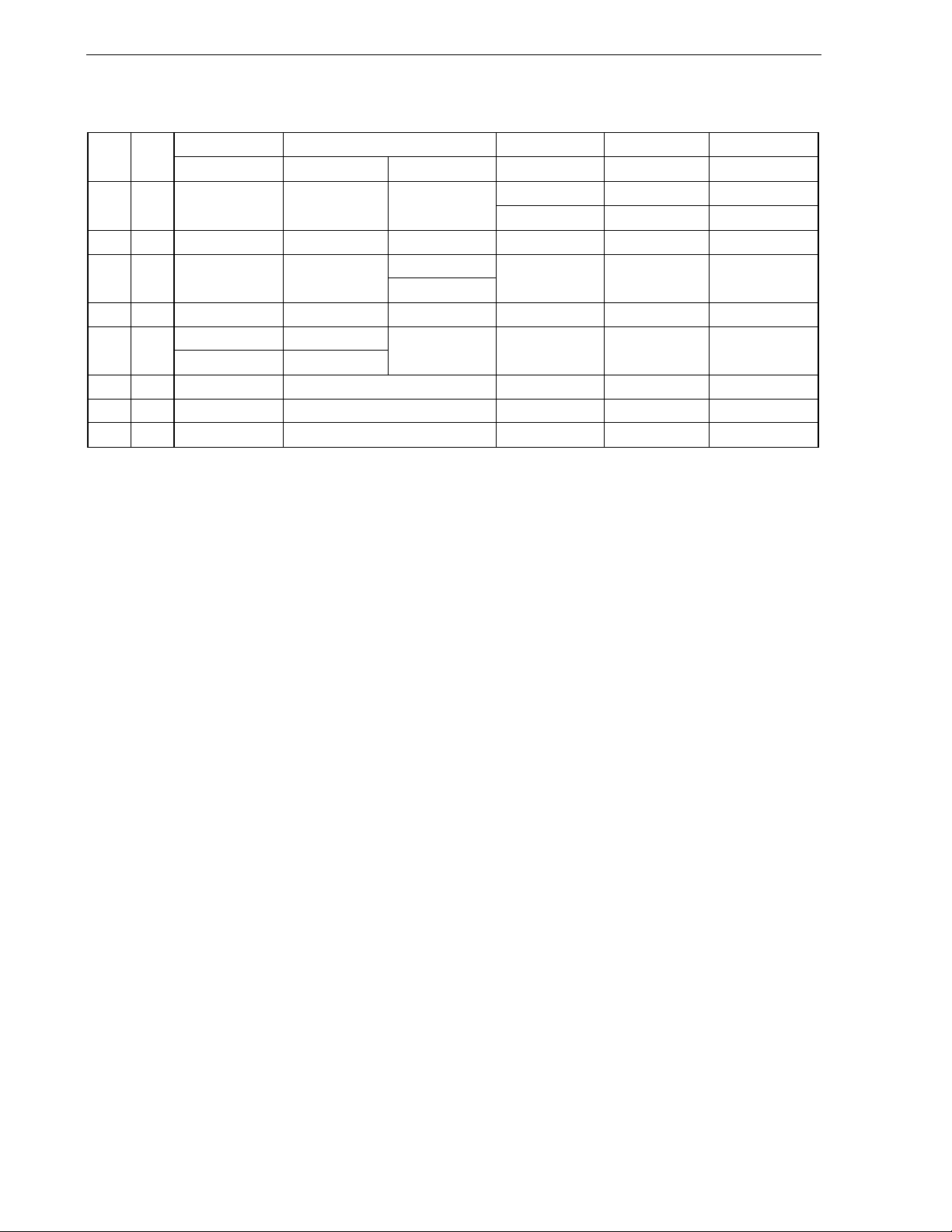
1.5 78K0/Kx2 Microcontroller Lineup
78K0/KB2 78K0/KC2 78K0/KD2 78K0/KE2 78K0/KF2 ROM RAM
30/36 Pins 38/44 Pins 48 Pins 52 Pins 64 Pins 80 Pins
128 KB 7 KB
96 KB 5 KB
60 KB 3 KB
48 KB 2 KB
32 KB 1 KB
24 KB 1 KB μPD78F0502
16 KB 768 B μPD78F0501
8 KB 512 B μPD78F0500
Note Product with on-chip debug function
− − −
− − −
− −
− −
μ
PD78F0503D
μ
PD78F0503
Note
μPD78F0513D
μ
PD78F0513
CHAPTER 1 OUTLINE
μ
PD78F0515D
Note
μ
PD78F0512
μ
PD78F0511
μ
PD78F0515
μ
PD78F0514
μ
PD78F0513
μ
Note
PD78F0527D
μ
PD78F0527
μ
PD78F0526
μ
PD78F0525
μ
PD78F0524
μ
PD78F0523
μ
PD78F0522
μ
PD78F0521
Note
μ
PD78F0537D
μ
PD78F0537
μ
PD78F0536
μ
PD78F0535
μ
PD78F0534
μ
PD78F0533
μ
PD78F0532
μ
PD78F0531
Note
− − − −
μPD78F0547D
μ
PD78F0547
μ
PD78F0546
μ
PD78F0545
μ
PD78F0544
−
−
−
Note
26
User’s Manual U17336EJ5V0UD
Page 27
<R>
<R>
<R>
<R>
<R>
CHAPTER 1 OUTLINE
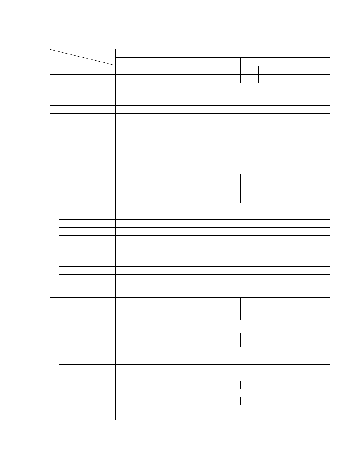
The list of functions of the 78K0/Kx2 microcontrollers is shown below.
(1/2)
78K0/KB2 78K0/KC2 Part Number
Item
Flash memory (KB) 8 16 24 32 16 24 32 16 24 32 48 60
RAM (KB) 0.5 0.75 1 1 0.75 1 1 0.75 1 1 2 3
Bank (flash memory)
Power supply voltage • Standard products, (A) grade products: VDD = 1.8 to 5.5 V
Regulator Provided
Minimum instruction
execution time
High-speed system 20 MHz: VDD = 4.0 to 5.5 V/10 MHz: VDD = 2.7 to 5.5 V/5 MHz: VDD = 1.8 to 5.5 V
Internal high-speed
Main
oscillation
Clock
Subsystem
Internal low-speed
oscillation
Total 23 31 (38 Pins)/
Port
N-ch O.D. (6 V
tolerance)
16 bits (TM0) 1 ch
8 bits (TM5) 2 ch
8 bits (TMH) 2 ch
Timer
Watch
WDT 1 ch
3-wire CSI
Automatic transmit/
receive 3-wire CSI
UART/3-wire CSI
UART supporting LIN-
Serial interface
bus
I2C bus 1 ch
10-bit A/D 4 ch 6 ch (38 Pins)/
External 6 7 8
Internal 14 16
Interrupt
Key interrupt
RESET pin Provided
POC 1.59 V ±0.15 V (rise time to 1.8 V: 3.6 ms (MAX.))
Reset
LVI The detection level of the supply voltage is selectable in 16 steps.
WDT Provided
Clock output/buzzer output
Multiplier/divider
On-chip debug function
Operating ambient
temperature
Note
1 ch
30/36 Pins 38/44 Pins 48 Pins
−
0.1 μs (20 MHz: VDD = 4.0 to 5.5 V)/0.2 μs (10 MHz: VDD = 2.7 to 5.5 V)/
−
2 4 4
−
−
μ
PD78F0503D only
• Standard products, (A) grade products: TA = –40 to +85°C
• (A2) grade products: T
• (A2) grade products: V
μ
s (5 MHz: VDD = 1.8 to 5.5 V)
0.4
8 MHz (TYP.): VDD = 1.8 to 5.5 V
240 kHz (TYP.): VDD = 1.8 to 5.5 V
37 (44 Pins)
8 ch (44 Pins)
2 ch (38 Pins)/
4 ch (44 Pins)
−
−
μ
PD78F0513D only
A = –40 to +110°C, TA = –40 to +125°C
DD = 2.7 to 5.5 V
32.768 kHz (TYP.): VDD = 1.8 to 5.5 V
1 ch
−
−
1 ch
Clock output only
μ
PD78F0515D only
41
8 ch
4 ch
Provided
Note Select either of the functions of these alternate-function pins.
User’s Manual U17336EJ5V0UD
27
Page 28
CHAPTER 1 OUTLINE
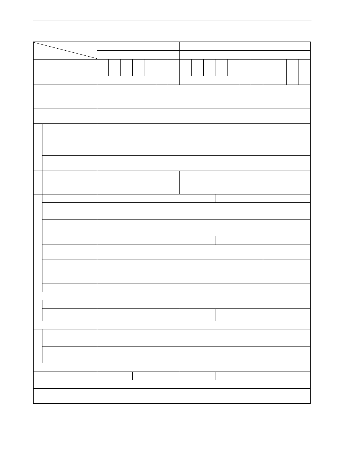
(2/2)
78K0/KD2 78K0/KE2 78K0/KF2 Part Number
Item
52 Pins 64 Pins 80 Pins
Flash memory (KB) 16 24 32 48 60 96 128 16 24 32 48 60 96 128 48 60 96 128
RAM (KB) 0.75 1 1 2 3 5 7 0.75 1 1 2 3 5 7 2 3 5 7
Bank (flash memory)
Power supply voltage • Standard products, (A) grade products: VDD = 1.8 to 5.5 V
<R>
−
4 6
• (A2) grade products: V
−
DD = 2.7 to 5.5 V
4 6
−
4 6
Regulator Provided
Minimum instruction
execution time
0.1 μs (20 MHz: VDD = 4.0 to 5.5 V)/0.2 μs (10 MHz: VDD = 2.7 to 5.5 V)/
0.4
μ
s (5 MHz: VDD = 1.8 to 5.5 V)
High-speed system 20 MHz: VDD = 4.0 to 5.5 V/10 MHz: VDD = 2.7 to 5.5 V/5 MHz: VDD = 1.8 to 5.5 V
Internal high-speed
Main
oscillation
Clock
Subsystem 32.768 kHz (TYP.): VDD = 1.8 to 5.5 V
Internal low-speed
8 MHz (TYP.): VDD = 1.8 to 5.5 V
240 kHz (TYP.): VDD = 1.8 to 5.5 V
oscillation
Total 45 55 71
N-ch O.D. (6 V
Port
4 4 4
tolerance)
16 bits (TM0) 1 ch 2 ch
8 bits (TM5) 2 ch
8 bits (TMH) 2 ch
Timer
Watch 1 ch
WDT 1 ch
3-wire CSI
Automatic transmit/
−
−
1 ch
1 ch
receive 3-wire CSI
UART/3-wire CSI
UART supporting LIN-
Serial interface
bus
Note
1 ch
1 ch
I2C bus 1 ch
10-bit A/D 8 ch
External 8 9
Internal 16 19 20
Interrupt
Key interrupt 8 ch
RESET pin Provided
POC 1.59 V ±0.15 V (rise time to 1.8 V: 3.6 ms (MAX.))
Reset
LVI The detection level of the supply voltage is selectable in 16 steps.
WDT Provided
Clock output/buzzer output Clock output only Provided
Multiplier/divider
On-chip debug function
Operating ambient
<R>
temperature
−
μ
PD78F0527D only
Provided
−
μ
PD78F0537D only
Provided
• Standard products, (A) grade products: TA = –40 to +85°C
• (A2) grade products: T
A = –40 to +110°C, TA = –40 to +125°C
μ
PD78F0547D only
Note Select either of the functions of these alternate-function pins.
28
User’s Manual U17336EJ5V0UD
Page 29
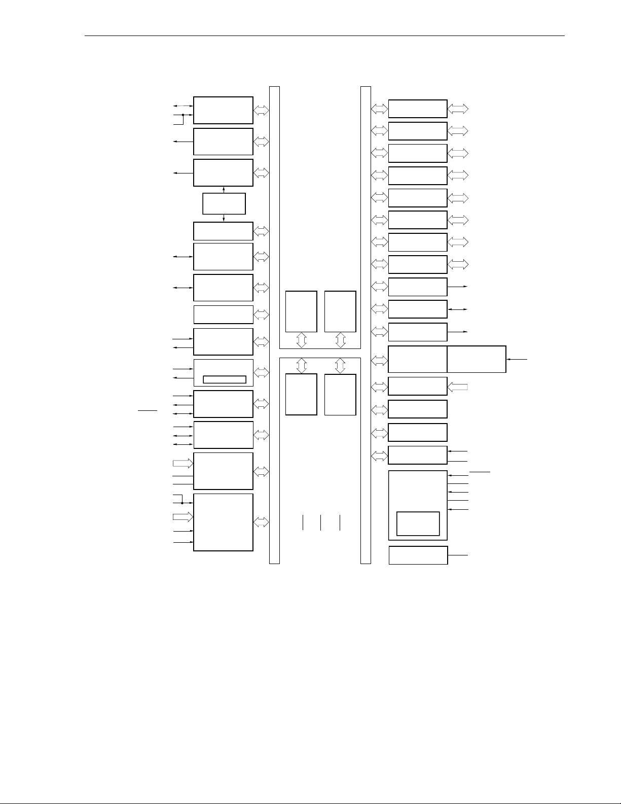
1.6 Block Diagram
CHAPTER 1 OUTLINE
<R>
TO00/TI010/P01
TI000/P00
16-bit timer/
event counter 00
RxD6/P14 (LINSEL)
TOH0/P15
TOH1/P16
8-bit timer H0
8-bit timer H1
Internal
low-speed
oscillator
Watchdog timer
TI50/TO50/P17
TI51/TO51/P33
RxD0/P11
TxD0/P10
RxD6/P14
TxD6/P13
SI10/P11
SO10/P12
SCK10/P10
EXSCL0/P62
SDA0/P61
8-bit timer/
event counter 50
8-bit timer/
event counter 51
Watch timer
Serial
interface UART0
Serial
interface UART6
LINSEL
Serial
interface CSI10
Serial interface IIC0
78K/0
CPU
core
Internal
high-speed
RAM
SCL0/P60
ANI0/P20 to ANI5/P25,
Note 1
ANI6/P26
, ANI7/P27
AV
Note 1
AV
8
REF
SS
A/D converter
RxD6/P14 (LINSEL)
INTP0/P120
INTP1/P30 to
INTP4/P33
INTP5/P16
INTP6/P140
Note 2
4
Interrupt control
DD
Notes 1. Available only in the 44-pin and 48-pin products.
2 Available only in the 48-pin products.
3. Available only in the
4. Available only in the
μ
PD78F0514, 78F0515, and 78F0515D.
μ
PD78F0513D and 78F0515D.
VSSFLMD0 V
Flash
memory
Internal
expansion
Note 3
RAM
Port 0
Port 1
Port 2
Port 3
Port 4
Port 6
Port 7
Port 12
Note 2
Port 13
Note 2
Port 14
Clock output
Note 2
control
Power-on-clear/
low-voltage
indicator
Key return
Reset control
Multiplier &
Note 3
divider
On-chip debug
System control
Internal
high-speed
oscillator
Voltage regulator
Note 4
2
P00, P01
8
P10 to P17
8
P20 to P25, P26
4
P30 to P33
Note 1
2
P40
4
P60 to P63
P70, P71, P72
6
Note 1
P73
5
P120 to P124
Note 2
P130
Note 2
P140
PCL/P140
POC/LVI
control
KR0/P70, KR1/P71,
4
KR2/P72
Note 4
OCD0A
Note 4
OCD0B
RESET
X1/P121
X2/EXCLK/P122
XT1/P123
XT2/EXCLKS/P124
REGC
Note 1
, P41
Note 2
, P74
Note 2
Note 1
, KR3/P73
/X1, OCD1A
/X2, OCD1B
Note 1
Note 1
, P27
,
Note 2
, P75
EXLVI/P120
Note 1
Note 4
Note 4
Note 1
/P31
/P32
User’s Manual U17336EJ5V0UD
29
Page 30
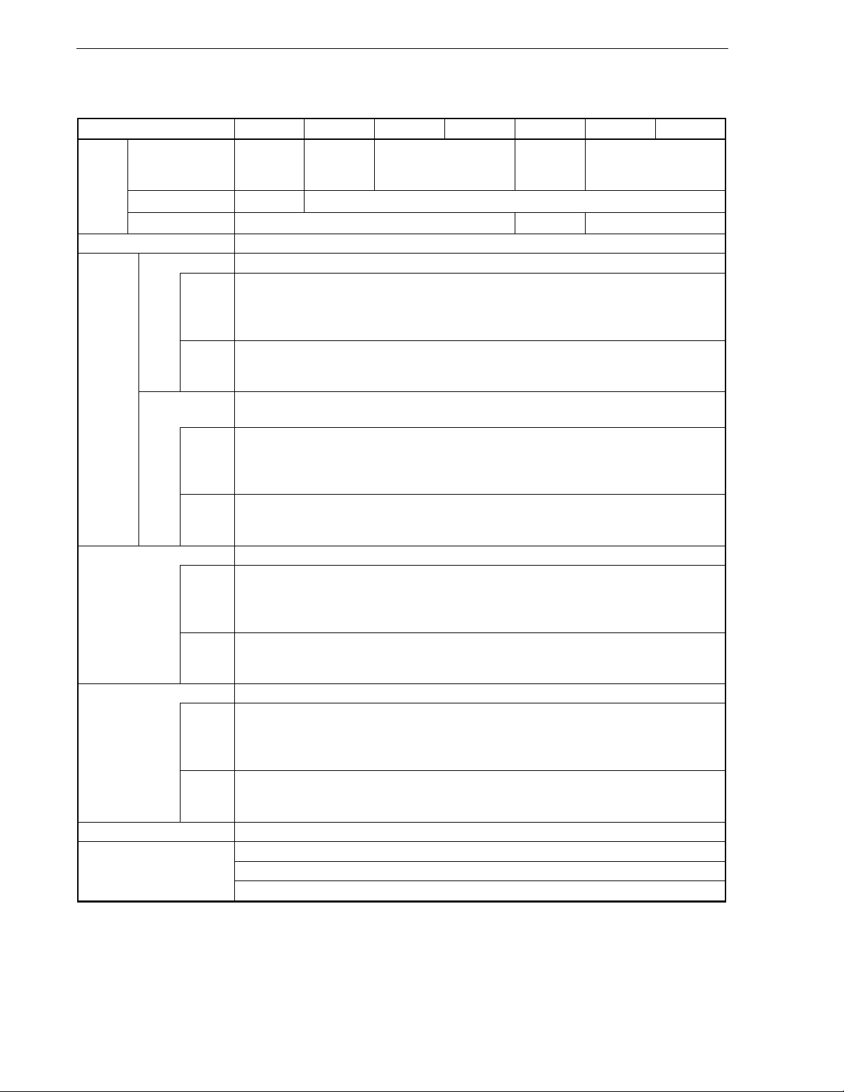
CHAPTER 1 OUTLINE
1.7 Outline of Functions
(1/2)
Item
Internal
memory
(bytes)
Flash memory
(self-programming
supported)
Note
High-speed RAM
Expansion RAM
Memory space 64 KB
Main
system
clock
(oscillation
frequency)
High-speed
system
Standard
clock
products,
(A) grade
products
(A2)
grade
products
Internal highspeed oscillation
clock
Standard
products,
(A) grade
products
(A2)
grade
products
Subsystem clock XT1 (crystal) oscillation, external subsystem clock input (EXCLKS)
(oscillation
frequency)
Standard
products,
(A) grade
products
(A2)
grade
products
Internal low-speed Internal oscillation
oscillation clock
(for TMH1, WDT)
Standard
products,
(A) grade
products
(A2)
grade
products
General-purpose registers 8 bits × 32 registers (8 bits × 8 registers × 4 banks)
Minimum instruction execution
time
Note The internal flash memory capacity, internal high-speed RAM capacity, and internal expansion RAM capacity
can be changed using the internal memory size switching register (IMS) and the internal expansion RAM size
switching register (IXS).
μ
PD78F0511 μPD78F0512 μPD78F0513 μPD78F0513DμPD78F0514 μPD78F0515 μPD78F0515D
16 K 24 K 32 K 48 K 60 K
Note
768
Note
1 K
−
1 K 2 K
X1 (crystal/ceramic) oscillation, external main system clock input (EXCLK)
1 to 20 MHz: VDD = 4.0 to 5.5 V, 1 to 10 MHz: VDD = 2.7 to 5.5 V,
1 to 5 MHz: V
DD = 1.8 to 5.5 V
1 to 20 MHz: V
DD = 4.0 to 5.5 V, 1 to 10 MHz: VDD = 2.7 to 5.5 V
Internal oscillation
8 MHz (TYP.): VDD = 1.8 to 5.5 V
8 MHz (TYP.): V
32.768 kHz (TYP.): V
32.768 kHz (TYP.): V
240 kHz (TYP.): V
240 kHz (TYP.): V
DD = 2.7 to 5.5 V
DD = 1.8 to 5.5 V
DD = 2.7 to 5.5 V
DD = 1.8 to 5.5 V
DD = 2.7 to 5.5 V
0.1 μs (high-speed system clock: @ fXH = 20 MHz operation)
0.25 μs (internal high-speed oscillation clock: @ fRH = 8 MHz (TYP.) operation)
122
μ
s (subsystem clock: @ fSUB = 32.768 kHz operation)
30
User’s Manual U17336EJ5V0UD
Page 31
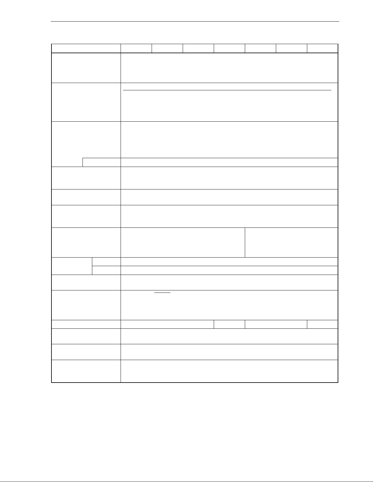
<R>
<R>
<R>
CHAPTER 1 OUTLINE
Item
μ
PD78F0511 μPD78F0512 μPD78F0513 μPD78F0513DμPD78F0514 μPD78F0515 μPD78F0515D
Instruction set • 8-/16-bit operation
• Multiply/divide (8 bits × 8 bits, 16 bits ÷ 8 bits)
• Bit manipulate (set, reset, test, and Boolean operation)
• BCD adjust, etc.
I/O ports
Total: 31 (38-pin products) 37 (44-pin products) 41 (48-pin products)
CMOS I/O: 27 33 36
CMOS output: 0 0 1
N-ch open-drain I/O
(6 V tolerance): 4 4 4
Timers • 16-bit timer/event counter: 1 channel
• 8-bit timer/event counter: 2 channels
• 8-bit timer: 2 channels
• Watch timer: 1 channel
• Watchdog timer: 1 channel
Timer outputs 5 (PWM output: 4, PPG output: 1)
Clock output
(48-pin products only)
• 156.25 kHz, 312.5 kHz, 625 kHz, 1.25 MHz, 2.5 MHz, 5 MHz, 10 MHz
(peripheral hardware clock: @ f
• 32.768 kHz (subsystem clock: @ f
PRS = 20 MHz operation)
SUB = 32.768 kHz operation)
A/D converter • 38-pin products: 10-bit resolution × 6 channels (AVREF = 2.3 to 5.5 V)
• 44-pin, 48-pin products: 10-bit resolution × 8 channels (AV
Serial interface • UART mode supporting LIN-bus: 1 channel
• 3-wire serial I/O mode/UART mode
2
• I
C bus mode: 1 channel
Multiplier/divider
−
Note
: 1 channel
REF = 2.3 to 5.5 V)
• 16 bits × 16 bits = 32 bits
(multiplication)
• 32 bits ÷ 16 bits = 32 bits
remainder of 16 bits (division)
Internal 16 Vectored
interrupt sources
External 7 (38-pin, 44-pin products), 8 (48-pin products)
Key interrupt Key interrupt (INTKR) occurs by detecting falling edge of key input pins (KR0 and KR1 (38-pin
products), KR0 to KR3 (44-pin, 48-pin products)).
Reset • Reset using RESET pin
• Internal reset by watchdog timer
• Internal reset by power-on-clear
• Internal reset by low-voltage detector
On-chip debug function
−
Provided
−
Provided
Power supply voltage • Standard products, (A) grade products: VDD = 1.8 to 5.5 V
Operating ambient
temperature
• (A2) grade products: V
• Standard products, (A) grade products: TA = –40 to +85°C
• (A2) grade products: T
DD = 2.7 to 5.5 V
A = –40 to +110°C, TA = –40 to +125°C
Package • 38-pin plastic SSOP (7.62 mm (300))
• 44-pin plastic LQFP (10 × 10)
• 48-pin plastic LQFP (fine pitch) (7 × 7)
Note Select either of the functions of these alternate-function pins.
(2/2)
User’s Manual U17336EJ5V0UD
31
Page 32
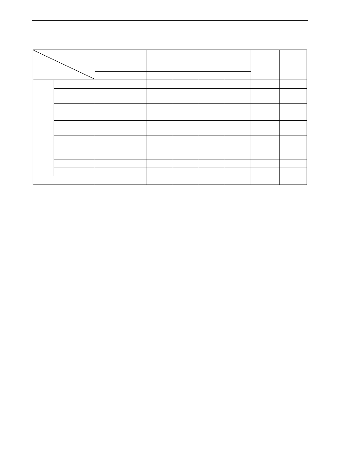
CHAPTER 1 OUTLINE
An outline of the timer is shown below.
16-bit Timer/
Event Counter
00
8-bit Timer/
Event Counters
50 and 51
8-bit Timers H0 and H1
Watch
Timer
TM00 TM50 TM51 TMH0 TMH1
Function
Interval timer 1 channel 1 channel 1 channel 1 channel 1 channel 1 channel
External event
1 channel 1 channel 1 channel
− − − −
counter
PPG output 1 output
PWM output
Pulse width
−
2 inputs
− − − − − −
1 output 1 output 1 output 1 output
− −
− − − − − −
measurement
Square-wave
1 output 1 output 1 output 1 output 1 output
− −
output
Carrier generator
Watch timer
Watchdog timer
− − − −
− − − − −
− − − − − −
1 output
Note 2
− −
1 channel
Interrupt source 2 1 1 1 1 1
Note 1
Note 1
Watchdog
1 channel
Notes 1. In the watch timer, the watch timer function and interval timer function can be used simultaneously.
2. TM51 and TMH1 can be used in combination as a carrier generator mode.
Timer
−
−
−
32
User’s Manual U17336EJ5V0UD
Page 33
<R>
CHAPTER 2 PIN FUNCTIONS
2.1 Pin Function List
There are two types of pin I/O buffer power supplies: AV
supplies and the pins is shown below.
Table 2-1. Pin I/O Buffer Power Supplies
Power Supply Corresponding Pins
AVREF P20 to P27
VDD Pins other than P20 to P27
(1) Port functions (1/2)
Function Name I/O Function After Reset Alternate Function
P00 TI000
I/O
P01
Port 0.
2-bit I/O port.
Input/output can be specified in 1-bit units.
Use of an on-chip pull-up resistor can be specified by a software
setting.
P10 SCK10/TxD0
I/O
P11 SI10/RxD0
P12 SO10
P13 TxD6
Port 1.
8-bit I/O port.
Input/output can be specified in 1-bit units.
Use of an on-chip pull-up resistor can be specified by a software
setting.
P14 RxD6
P15 TOH0
P16 TOH1/INTP5
P17
P20 to P25 ANI0 to ANI7
Note 1
P26
, P27
Note 1
I/O
Port 2.
8-bit I/O port.
Input/output can be specified in 1-bit units.
P30 INTP1
I/O
P31 INTP2/OCD1A
P32 INTP3/OCD1B
P33
Port 3.
4-bit I/O port.
Input/output can be specified in 1-bit units.
Use of an on-chip pull-up resistor can be specified by a software
setting.
Notes 1. 44-pin and 48-pin products only
For the 38-pin products, be sure to set bits 6 and 7 of PM2 to “1”, and bits 6 and 7 of P2 to “0”.
2.
μ
PD78F0513D and 78F0515D only
REF and VDD. The relationship between these power
Input port
TI010/TO00
Input port
TI50/TO50
Analog input
Note 1
ANI6
, ANI7
Input port
TI51/TO51/INTP4
Note 1
Note 2
Note 2
User’s Manual U17336EJ5V0UD
33
Page 34
CHAPTER 2 PIN FUNCTIONS
(1) Port functions (2/2)
Function Name I/O Function After Reset Alternate Function
Note 1
P40
and
Note 1
P41
P60 SCL0
I/O
I/O
P61 SDA0
P62 EXSCL0
P63
P70, P71 KR0, KR1
Note 1
P72
and
Note 1
P73
Note 2
P74
and
Note 2
P75
P120 INTP0/EXLVI
I/O
I/O
P121 X1/OCD0A
P122
P123 XT1
P124
Note 2
P130
P140
Output
Note 2
I/O
Port 4.
2-bit I/O port.
Input/output can be specified in 1-bit units.
Use of an on-chip pull-up resistor can be specified by a
software setting.
Port 6.
4-bit I/O port.
Output of P60 to P63 is N-ch open-drain output (6 V tolerance).
Input/output can be specified in 1-bit units.
Port 7.
6-bit I/O port.
Input/output can be specified in 1-bit units.
Use of an on-chip pull-up resistor can be specified by a
software setting.
Port 12.
5-bit I/O port.
Input/output can be specified in 1-bit units.
Only for P120, use of an on-chip pull-up resistor can be
specified by a software setting.
Port 13.
1-bit output-only port.
Port 14.
1-bit I/O port.
Input/output can be specified in 1-bit units.
Use of an on-chip pull-up resistor can be specified by a
software setting.
Input port
Input port
Input port
Note 1
and
KR2
Note 1
KR3
Input port
X2/EXCLK/OCD0B
XT2/EXCLKS
Output port
Input port PCL/INTP6
−
−
−
Note 3
−
Note 2
Note 3
Notes 1. 44-pin and 48-pin products only
<R>
For the 38-pin products, be sure to set bits 0 and 1 of PM4, bits 2 and 3 of PM7, bits 0 and 1 of P4, and bits
2 and 3 of P7 to “0”.
2. 48-pin products only
3.
μ
PD78F0513D and 78F0515D only
34
User’s Manual U17336EJ5V0UD
Page 35
<R>
CHAPTER 2 PIN FUNCTIONS
(2) Non-port functions (1/2)
Function Name I/O Function After Reset Alternate Function
ANI0 to ANI5 P20 to P25
Note 1
ANI6
, ANI7
Input A/D converter analog input Analog input
Note 1
P26
Note 1
, P27
Note 1
EXLVI Input Potential input for external low-voltage detection Input port P120/INTP0
EXSCL0 Input
External clock input for serial interface.
Input port P62
To input an external clock, input a clock of 6.4 MHz.
FLMD0
INTP0 P120/EXLVI
Input
INTP1 P30
INTP2 P31/OCD1A
INTP3 P32/OCD1B
Flash memory programming mode setting
−
External interrupt request input for which the valid edge (rising
edge, falling edge, or both rising and falling edges) can be
specified
− −
Input port
Note 2
Note 2
INTP4 P33/TI51/TO51
INTP5 P16/TOH1
Note 3
INTP6
KR0, KR1 P70, P71
KR2
KR3
PCL
Input Key interrupt input Input port
Note 1
and
Note 1
Note 3
Output
Clock output (for trimming of high-speed system clock,
P140/PCL
P72
P73
Input port P140/INTP6
Note 1
Note 1
Note 3
and
Note 3
subsystem clock)
REGC
Connecting regulator output (2.5 V) stabilization capacitance
−
− −
for internal operation.
Connect to V
SS via a capacitor (0.47 to 1
RESET Input System reset input
RxD0 P11/SI10
Input Serial data input to asynchronous serial interface Input port
RxD6
SCK10 P10/TxD0
I/O Clock input/output for serial interface Input port
SCL0
μ
F: recommended).
− −
P14
P60
SDA0 I/O Serial data I/O for serial interface Input port P61
SI10 Input Serial data input to serial interface Input port P11/RxD0
SO10 Output Serial data output from serial interface Input port P12
TI000
Input
External count clock input to 16-bit timer/event counter 00
Input port
P00
Capture trigger input to capture registers (CR000, CR010) of
16-bit timer/event counter 00
TI010
Capture trigger input to capture register (CR000) of 16-bit
P01/TO00
timer/event counter 00
TI50 External count clock input to 8-bit timer/event counter 50 P17/TO50
TI51
Input
External count clock input to 8-bit timer/event counter 51
Input port
P33/TO51/INTP4
TO00 Output 16-bit timer/event counter 00 output Input port P01/TI010
Notes 1. 44-pin and 48-pin products only
For the 38-pin products, be sure to set bits 6 and 7 of PM2 to “1”, and bits 2 and 3 of PM7, bits 6 and 7 of
P2, and bits 2 and 3 of P7 to “0”.
2.
μ
PD78F0513D and 78F0515D only
3. 48-pin products only
User’s Manual U17336EJ5V0UD
35
Page 36
CHAPTER 2 PIN FUNCTIONS
(2) Non-port pins (2/2)
Function Name I/O Function After Reset Alternate Function
TO50 8-bit timer/event counter 50 output P17/TI50
TO51
TOH0 8-bit timer H0 output P15
TOH1
TxD0 P10/SCK10
TxD6
X1 Input
X2
EXCLK Input External clock input for main system clock Input port P122/X2/
XT1 Input Input port P123
XT2
EXCLKS Input External clock input for subsystem clock Input port P124/XT2
VDD
AVREF Input
VSS
AVSS
Note
OCD0A
OCD1A
OCD0B
OCD1B
Note
Note
Note
Output
8-bit timer/event counter 51 output
Output
8-bit timer H1 output
Output Serial data output from asynchronous serial interface Input port
Connecting resonator for main system clock Input port
−
Connecting resonator for subsystem clock
−
Positive power supply for pins other than P20 to P27
−
A/D converter reference voltage input and positive power
supply for P20 to P27 and A/D converter
Ground potential for pins other than P20 to P27
−
A/D converter ground potential. Make the same potential as
−
SS.
V
Input
Connection for on-chip debug mode setting pins
μ
PD78F0513D and 78F0515D only)
(
−
Input port
Input port
Input port P124/EXCLKS
− −
− −
− −
− −
Input port
P33/TI51/INTP4
P16/INTP5
P13
Note
Note
Note
P121/OCD0A
P122/EXCLK/
OCD0B
OCD0B
P121/X1
P31/INTP2
P122/X2/EXCLK
P32/INTP3
Note
μ
PD78F0513D and 78F0515D only
2.2 Description of Pin Functions
2.2.1 P00 and P01 (port 0)
P00 and P01 function as a 2-bit I/O port. These pins also function as timer I/O.
The following operation modes can be specified in 1-bit units.
(1) Port mode
P00 and P01 function as a 2-bit I/O port. P00 and P01 can be set to input or output port in 1-bit units using port
mode register 0 (PM0). Use of an on-chip pull-up resistor can be specified by pull-up resistor option register 0
(PU0).
(2) Control mode
P00 and P01 function as timer I/O.
(a) TI000
This is a pin for inputting an external count clock to 16-bit timer/event counter and is also for inputting a
capture trigger signal to the capture registers (CR000, CR010) of 16-bit timer/event counter 00.
36
User’s Manual U17336EJ5V0UD
Page 37

CHAPTER 2 PIN FUNCTIONS
(b) TI010
This is a pin for inputting a capture trigger signal to the capture register (CR000) of 16-bit timer/event counter
00.
(c) TO00
This is a timer output pin of 16-bit timer/event counter 00.
2.2.2 P10 to P17 (port 1)
P10 to P17 function as an 8-bit I/O port. These pins also function as pins for external interrupt request input, serial
interface data I/O, clock I/O, and timer I/O.
The following operation modes can be specified in 1-bit units.
(1) Port mode
P10 to P17 function as an 8-bit I/O port. P10 to P17 can be set to input or output port in 1-bit units using port
mode register 1 (PM1). Use of an on-chip pull-up resistor can be specified by pull-up resistor option register 1
(PU1).
(2) Control mode
P10 to P17 function as external interrupt request input, serial interface data I/O, clock I/O, and timer I/O.
(a) SI10
This is a serial data input pin of serial interface CSI10.
(b) SO10
This is a serial data output pin of serial interface CSI10.
(c) SCK10
This is a serial clock I/O pin of serial interface CSI10.
(d) RxD0
This is a serial data input pin of serial interface UART0.
(e) RxD6
This is a serial data input pin of serial interface UART6.
(f) TxD0
This is a serial data output pin of serial interface UART0.
(g) TxD6
This is a serial data output pin of serial interface UART6.
(h) TI50
This is the pin for inputting an external count clock to 8-bit timer/event counter 50.
(i) TO50
This is a timer output pin of 8-it timer/event counter 50.
User’s Manual U17336EJ5V0UD
37
Page 38

(j) TOH0, TOH1
These are the timer output pins of 8-bit timers H0 and H1.
(k) INTP5
This is an external interrupt request input pin for which the valid edge (rising edge, falling edge, or both rising
and falling edges) can be specified.
2.2.3 P20 to P27 (port 2)
P20 to P27 function as an 8-bit I/O port. These pins also function as pins for A/D converter analog input.
The following operation modes can be specified in 1-bit units.
(1) Port mode
P20 to P27 function as an 8-bit I/O port. P20 to P27 can be set to input or output port in 1-bit units using port
mode register 2 (PM2).
(2) Control mode
P20 to P27 function as A/D converter analog input pins (ANI0 to ANI7). When using these pins as analog input
pins, see (5) ANI0/P20 to ANI7/P27 in 12.6 Cautions for A/D Converter.
<R>
Cautions 1. For the 38-pin products, be sure to set bits 6 and 7 of PM2 to “1”, and bits 6 and 7 of P2 to
2. ANI0/P20 to ANI7/P27 are set in the analog input mode after release of reset.
<R>
Remark 38-pin products: ANI0/P20 to ANI5/P05
44-pin and 48-pin products: ANI0/P20 to ANI7/P07
2.2.4 P30 to P33 (port 3)
P30 to P33 function as a 4-bit I/O port. These pins also function as pins for external interrupt request input and
timer I/O.
The following operation modes can be specified in 1-bit units.
(1) Port mode
P30 to P33 function as a 4-bit I/O port. P30 to P33 can be set to input or output port in 1-bit units using port
mode register 3 (PM3). Use of an on-chip pull-up resistor can be specified by pull-up resistor option register 3
(PU3).
(2) Control mode
P30 to P33 function as external interrupt request input and timer I/O.
(a) INTP1 to INTP4
These are the external interrupt request input pins for which the valid edge (rising edge, falling edge, or both
rising and falling edges) can be specified.
(b) TI51
This is an external count clock input pin to 8-bit timer/event counter 51.
CHAPTER 2 PIN FUNCTIONS
“0”.
38
User’s Manual U17336EJ5V0UD
Page 39

<R>
<R>
<R>
CHAPTER 2 PIN FUNCTIONS
(c) TO51
This is a timer output pin from 8-bit timer/event counter 51.
Cautions 1. In the products with an on-chip debug function (
to pull the P31/INTP2/OCD1A
Note
pin down before a reset release, to prevent malfunction.
μ
PD78F0513D and 78F0515D), be sure
2. For products without an on-chip debug function, with the flash memory of 48 KB or
more (
μ
PD78F0514 and 78F0515), and having a product rank of “I”, “K”, or “E”, and for
the products with an on-chip debug function (
P31/INTP2/OCD1A
Note
as follows when writing the flash memory with a flash memory
μ
PD78F0513D and 78F0515D), connect
programmer.
• P31/INTP2/OCD1A
Note
: Connect to VSS via a resistor (10 kΩ: recommended).
The above connection is not necessary when writing the flash memory by means of self
programming.
Note OCD1A is provided to the
μ
PD78F0513D and 78F0515D only.
Remarks 1. For the product ranks, consult an NEC Electronics sales representative.
2. Only for the
μ
PD78F0513D and 78F0515D, P31 and P32 can be used as on-chip debug mode
setting pins (OCD1A, OCD1B) when the on-chip debug function is used. For how to connect
an in-circuit emulator supporting on-chip debugging (QB-78K0MINI or QB-MINI2), see
CHAPTER 26 ON-CHIP DEBUG FUNCTION (
μ
PD78F0513D AND 78F0515D ONLY).
2.2.5 P40 and P41 (port 4) (44-pin and 48-pin products only)
P40 and P41 function as a 2-bit I/O port. P40 and P41 can be set to input or output port in 1-bit units using port
mode register 4 (PM4). Use of an on-chip pull-up resistor can be specified by pull-up resistor option register 4 (PU4).
Caution For the 38-pin products, be sure to set bits 0 and 1 of PM4 and P4 to “0”.
2.2.6 P60 to P63 (port 6)
P60 to P63 function as a 4-bit I/O port. These pins also function as pins for serial interface data I/O, clock I/O, and
external clock input.
The following operation modes can be specified in 1-bit units.
(1) Port mode
P60 to P63 function as a 4-bit I/O port. P60 to P63 can be set to input port or output port in 1-bit units using port
mode register 6 (PM6).
Output of P60 to P63 is N-ch open-drain output (6 V tolerance).
(2) Control mode
P60 to P63 function as serial interface data I/O, clock I/O, and external clock input.
(a) SDA0
This is a serial data I/O pin for serial interface IIC0.
(b) SCL0
This is a serial clock I/O pin for serial interface IIC0.
User’s Manual U17336EJ5V0UD
39
Page 40

Page 41

<R>
<R>
CHAPTER 2 PIN FUNCTIONS
(c) X1, X2
These are the pins for connecting a resonator for main system clock.
(d) EXCLK
This is an external clock input pin for main system clock.
(e) XT1, XT2
These are the pins for connecting a resonator for subsystem clock.
(f) EXCLKS
This is an external clock input pin for subsystem clock.
Caution For products without an on-chip debug function, with the flash memory of 48 KB or more
(
μ
PD78F0514 and 78F0515), and having a product rank of “I”, “K”, or “E”, and for the
product with an on-chip debug function (
P121/X1/OCD0A
Note
as follows when writing the flash memory with a flash memory
μ
PD78F0513D and 78F0515D), connect
programmer.
• P121/X1/OCD0A
Note
: When using this pin as a port, connect it to VSS via a resistor (10 kΩ:
recommended) (in the input mode) or leave it open (in the output
mode).
The above connection is not necessary when writing the flash memory by means of self
programming.
Note OCD0A is provided to the
μ
PD78F0513D and 78F0515D only.
Remarks 1. For the product ranks, consult an NEC Electronics sales representative.
2. Only for the
μ
PD78F0513D and 78F0515D, X1 and X2 can be used as on-chip debug mode
setting pins (OCD0A, OCD0B) when the on-chip debug function is used. For how to connect
an in-circuit emulator supporting on-chip debugging (QB-78K0MINI or QB-MINI2), see
CHAPTER 26 ON-CHIP DEBUG FUNCTION (
μ
PD78F0513D AND 78F0515D ONLY).
2.2.9 P130 (port 13) (48-pin products only)
P130 functions as a 1-bit output-only port.
Remark When the device is reset, P130 outputs a low level. Therefore, to output a high level from P130 before
the device is reset, the output signal of P130 can be used as a pseudo reset signal of the CPU (see the
figure for Remark in 4.2.9 Port 13 (48 pin products only)).
2.2.10 P140 (port 14) (48-pin products only)
P140 functions as a 1-bit I/O port. This pin also functions as external interrupt request input, and clock output.
The following operation modes can be specified in 1-bit units.
(1) Port mode
P140 functions as a 1-bit I/O port. P140 can be set to input or output port in 1-bit units using port mode register
14 (PM14). Use of an on-chip pull-up resistor can be specified by pull-up resistor option register 14 (PU14).
(2) Control mode
P140 functions as external interrupt request input, and clock output.
User’s Manual U17336EJ5V0UD
41
Page 42
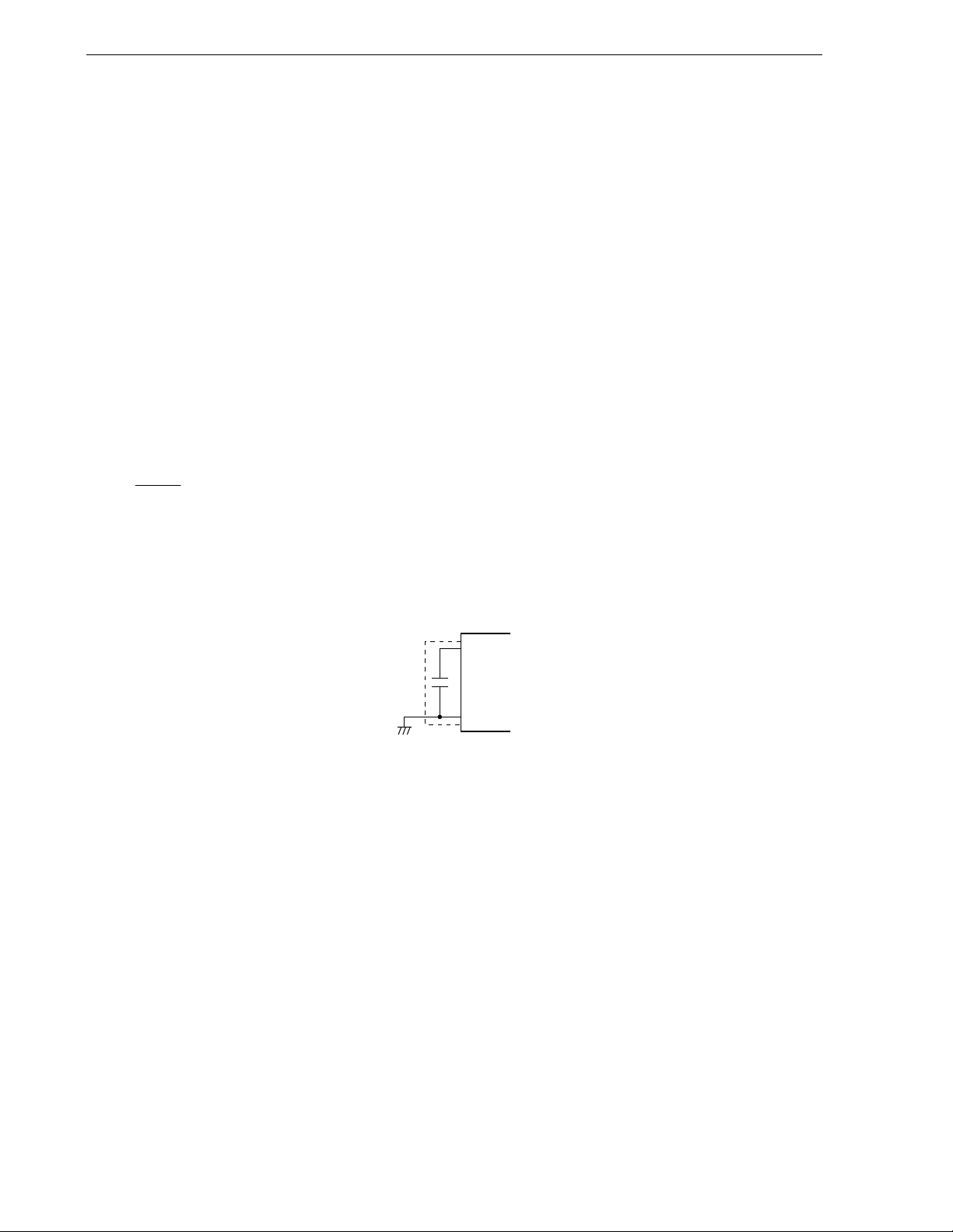
CHAPTER 2 PIN FUNCTIONS
(a) INTP6
This is an external interrupt request input pin for which the valid edge (rising edge, falling edge, or both rising
and falling edges) can be specified.
(b) PCL
This is a clock output pin.
2.2.11 AV
REF
This is the A/D converter reference voltage input pin and the positive power supply pin of P20 to P27 and A/D
converter.
When the A/D converter is not used, connect this pin directly to V
DD
Note
.
Note Make the AV
REF pin the same potential as the VDD pin when port 2 is used as a digital port.
2.2.12 AV
SS
This is the A/D converter ground potential pin. Even when the A/D converter is not used, always use this pin with
the same potential as the V
SS pin.
2.2.13 RESET
This is the active-low system reset input pin.
2.2.14 REGC
This is the pin for connecting regulator output (2.5 V) stabilization capacitance for internal operation. Connect this
pin to V
SS via a capacitor (0.47 to 1
μ
F: recommended).
REGC
SS
V
Caution Keep the wiring length as short as possible for the broken-line part in the above figure.
2.2.15 V
DD
VDD is the positive power supply pin for pins other than P20 to P27.
2.2.16 V
SS
V
SS is the ground potential pin for pins other than P20 to P27.
2.2.17 FLMD0
This is a pin for setting flash memory programming mode.
Connect FLMD0 to V
SS in the normal operation mode.
In flash memory programming mode, connect this pin to the flash memory programmer.
42
User’s Manual U17336EJ5V0UD
Page 43
<R>
<R>
CHAPTER 2 PIN FUNCTIONS
2.3 Pin I/O Circuits and Recommended Connection of Unused Pins
Table 2-2 shows the types of pin I/O circuits and the recommended connections of unused pins.
See Figure 2-1 for the configuration of the I/O circuit of each type.
Table 2-2. Pin I/O Circuit Types (1/2)
Pin Name I/O Circuit Type I/O Recommended Connection of Unused Pins
P00/TI000
P01/TI010/TO00
5-AH
I/O
Input: Independently connect to V
Output: Leave open.
P10/SCK10/TxD0
P11/SI10/RxD0
P12/SO10
5-AG
P13/TxD6
P14/RxD6 5-AH
P15/TOH0 5-AG
P16/TOH1/INTP5
5-AH
P17/TI50/TO50
ANI0/P20 to ANI5/P25
ANI6/P26,
ANI7/P27
Notes 1, 2
Note 1
11-G
<Analog setting>
Connect to AV
REF or AVSS.
<Digital setting>
Input: Independently connect to V
Output: Leave open.
P30/INTP1
P31/INTP2/OCD1A
P32/INTP3/OCD1B
Notes 3, 4
Note 4
5-AH
Input: Independently connect to V
Output: Leave open.
P33/TI51/TO51/INTP4
P40 and P41
P60/SCL0
P61/SDA0
P62/EXSCL0
Note 2
5-AG
13-AD
Input: Connect to V
SS.
Output: Leave this pin open at low-level output after clearing
the output latch of the port to 0.
P63 13-P
Notes 1. ANI0/P20 to ANI7/P27 are set to the analog input mode after a reset is released.
2. ANI6/P26, ANI7/P27, P40, and P41 are for 44-pin and 48-pin products only.
3. For products without an on-chip debug function, with the flash memory of 48 KB or more (
78F0515), and having a product rank of “I”, “K”, or “E”, and for the products with an on-chip debug function
(
μ
PD78F0513D and 78F0515D), connect P31/INTP2/OCD1A
Note 4
as follows when writing the flash memory
with a flash memory programmer.
• P31/INTP2/OCD1A
Note 4
: Connect to VSS via a resistor (10 kΩ: recommended).
The above connection is not necessary when writing the flash memory by means of self programming.
4. OCD1A and OCD1B are provided to the
μ
PD78F0513D and 78F0515D only.
Remark For the product ranks, consult an NEC Electronics sales representative.
DD or VSS via a resistor.
DD or VSS via a resistor.
DD or VSS via a resistor.
μ
PD78F0514 and
User’s Manual U17336EJ5V0UD
43
Page 44
CHAPTER 2 PIN FUNCTIONS
Table 2-2. Pin I/O Circuit Types (2/2)
Pin Name I/O Circuit Type I/O Recommended Connection of Unused Pins
P70/KR0, P71/KR1
P72/KR0, P73/KR3
P74, P75
Note 2
5-AH Input: Independently connect to V
Note 1
I/O
Output: Leave open.
P120/INTP0/EXLVI
Note 3
Notes 3, 4, 7
P121/X1/OCD0A
P122/X2/EXCLK/
Notes 3, 7
OCD0B
P123/XT1
P124/XT2/EXCLKS
Note 2
P130
P140/PCL/INTP6
3-C Output Leave open.
Note 2
37
Note 3
5-AH I/O
Input: Independently connect to V
Output: Leave open.
Input: Independently connect to V
Output: Leave open.
Note 6
Note 5
.
AVREF Connect directly to VDD
AVSS
FLMD0 38
RESET 2 Input Connect directly to VDD or via a resistor.
<R>
− −
Connect directly to VSS.
Connect to VSS
−
<R>
Notes 1. P72/KR0 and P73/KR3 are for 44-pin and 48-pin products only.
2. P74, P75, P130, and P140/PCL/INTP6 are for 48-pin products only.
3. Use recommended connection above in I/O port mode (see Figure 5-2 Format of Clock Operation
Mode Select Register (OSCCTL)) when these pins are not used.
<R>
4. For products without an on-chip debug function, with the flash memory of 48 KB or more (
and 78F0515), and having a product rank of “I”, “K”, or “E”, and for the product with an on-chip debug
function (
μ
PD78F0513D and 78F0515D), connect P121/X1/OCD0A
flash memory with a flash memory programmer.
• P121/X1/OCD0A
Note 7
: When using this pin as a port, connect it to VSS via a resistor (10 kΩ:
recommended) (in the input mode) or leave it open (in the output mode).
The above connection is not necessary when writing the flash memory by means of self programming.
5. Make the same potential as the V
DD pin when port 2 is used as a digital port.
6. FLMD0 is a pin that is used to write data to the flash memory. To rewrite the data of the flash memory
on-board, connect this pin to V
SS via a resistor (10 kΩ: recommended). The same applies when
executing on-chip debugging with a product with an on-chip debug function (μPD78F0513D and
78F0515D).
7. OCD0A and OCD0B are provided to the
μ
PD78F0513D and 78F0515D only.
Remark For the product ranks, consult an NEC Electronics sales representative.
DD or VSS via a resistor.
DD or VSS via a resistor.
DD or VSS via a resistor.
.
μ
Note 7
as follows when writing the
PD78F0514
44
User’s Manual U17336EJ5V0UD
Page 45
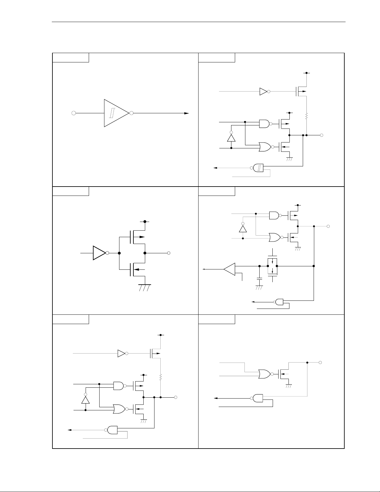
CHAPTER 2 PIN FUNCTIONS
Figure 2-1. Pin I/O Circuit List (1/2)
Type 2 Type 5-AH
V
DD
Pull-up
enable
V
DD
P-ch
IN
Schmitt-triggered input with hysteresis characteristics
Data
Output
disable
Input
enable
P-ch
N
-ch
V
SS
Type 3-C Type 11-G
REF
AV
Data
P-ch
N-ch
Data
V
DD
Output
disable
OUT
Comparator
V
SS
Series resistor string voltage
+
_
AV
P-ch
N-ch
SS
P-ch
N-ch
AV
SS
IN/OUT
IN/OUT
Input enable
Type 5-AG Type 13-P
DD
V
Pull-up
enable
Data
Output
disable
Input
enable
V
DD
V
SS
P-ch
N
-ch
P-ch
Data
Output
disable
IN/OUT
Input
enable
User’s Manual U17336EJ5V0UD
N-ch
V
SS
IN/OUT
45
Page 46
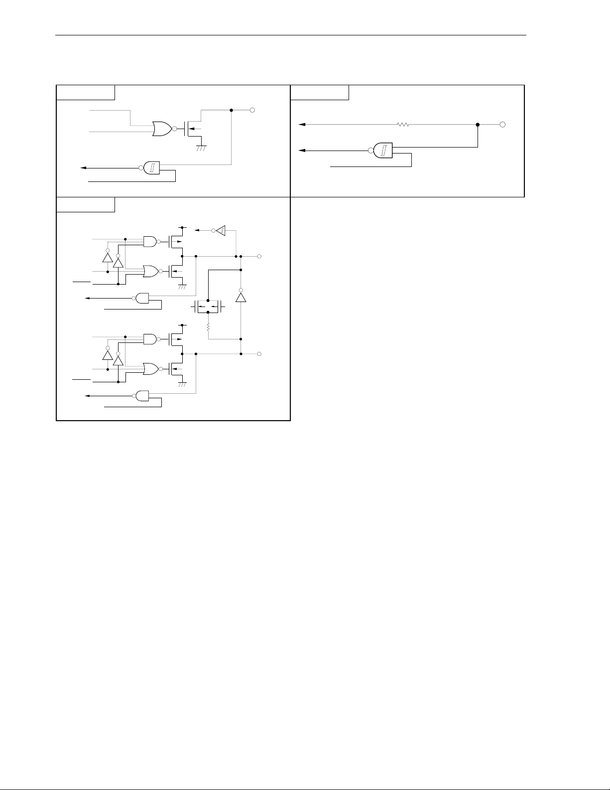
CHAPTER 2 PIN FUNCTIONS
Figure 2-1. Pin I/O Circuit List (2/2)
Type 13-AD Type 38
Data
Output
disable
N-ch
IN/OUT
IN
VSS
Input
enable
Type 37
V
DD
Data
Output
disable
RESET
Data
Output
disable
RESET
Input
enable
Input
enable
P-ch
N
-ch
V
SS
P-ch
N-ch
V
DD
P-ch
N
-ch
V
SS
X2,
XT2
X1,
XT1
Input
enable
46
User’s Manual U17336EJ5V0UD
Page 47
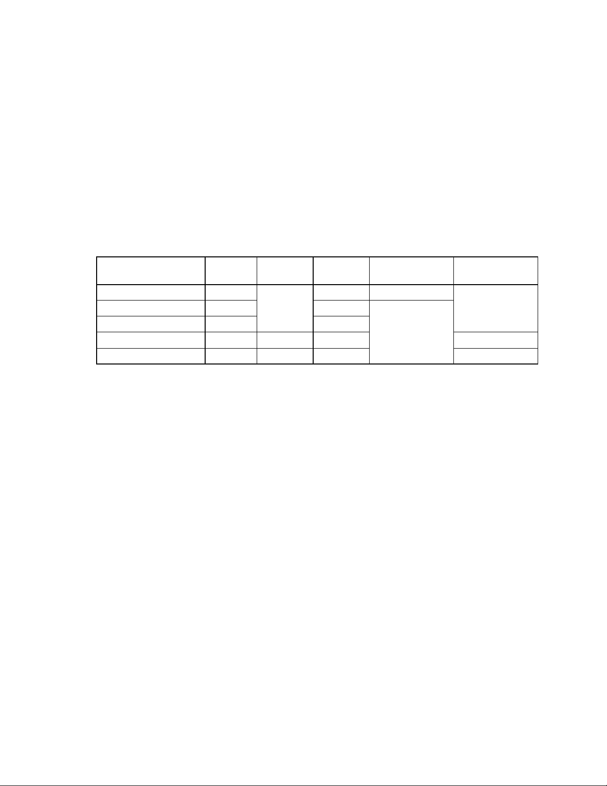
CHAPTER 3 CPU ARCHITECTURE
3.1 Memory Space
Products in the 78K0/KC2 can access a 64 KB memory space. Figures 3-1 to 3-7 show the memory maps.
Caution Regardless of the internal memory capacity, the initial values of the internal memory size
switching register (IMS) and internal expansion RAM size switching register (IXS) of all products
in the 78K0/KC2 are fixed (IMS = CFH, IXS = 0CH). Therefore, set the value corresponding to
each product as indicated below.
Table 3-1. Set Values of Internal Memory Size Switching Register (IMS)
and Internal Expansion RAM Size Switching Register (IXS)
<R>
Flash Memory Version
(78K0/KC2)
μ
PD78F0511 04H 16 KB 768 bytes
μ
PD78F0512 C6H 24 KB
μ
PD78F0513, 78F0513D
μ
PD78F0514 CCH 0AH 48 KB 1 KB
μ
PD78F0515, 78F0515D
Note
Note
IMS IXS
0CH
C8H
CFH 08H 60 KB
ROM
Capacity
32 KB
Internal High-Speed
RAM Capacity
1 KB
Internal Expansion
RAM Capacity
−
2 KB
Note The ROM and RAM capacities of the products with the on-chip debug function can be debugged by setting
IMS and IXS, according to the debug target products. Set IMS and IXS according to the debug target
products.
User’s Manual U17336EJ5V0UD
47
Page 48
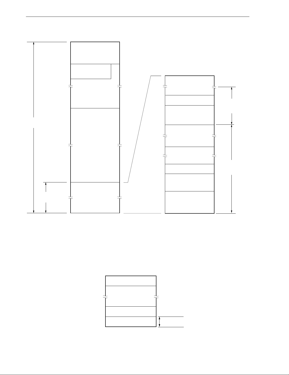
CHAPTER 3 CPU ARCHITECTURE
Figure 3-1. Memory Map (μPD78F0511)
FFFFH
Special function registers
FF00H
FEFFH
FEE0H
FEDFH
FC00H
FBFFH
Data memory
space
4000H
3FFFH
Program
memory space
0000H
(SFR)
256 × 8 bits
General-purpose
registers
32 × 8 bits
Internal high-speed RAM
768 × 8 bits
Reserved
Flash memory
16384 × 8 bits
3FFFH
1085H
1084H
1080H
107FH
1000H
0FFFH
0800H
07FFH
0085H
0084H
0080H
007FH
0040H
003FH
0000H
Program area
Option byte area
5 x 8 bits
Program area
CALLF entry area
2048 x 8 bits
Program area
1915 x 8 bits
Option byte area
5 x 8 bits
CALLT table area
64 x 8 bits
Vector table area
64 x 8 bits
Note 1
Note 1
1FFFH
Boot cluster 1
Boot cluster 0
Notes 1. When boot swap is not used: Set the option bytes to 0080H to 0084H.
When boot swap is used: Set the option bytes to 0080H to 0084H and 1080H to 1084H.
2. Writing boot cluster 0 can be prohibited depending on the setting of security (see 25.8 Security
Setting).
Remark The flash memory is divided into blocks (one block = 1 KB). For the address values and block numbers,
see Table 3-2 Correspondence Between Address Values and Block Numbers in Flash Memory.
3FFFH
3C00H
3BFFH
Block 0FH
Note 2
48
07FFH
0400H
03FFH
0000H
Block 01H
Block 00H
1 KB
User’s Manual U17336EJ5V0UD
Page 49
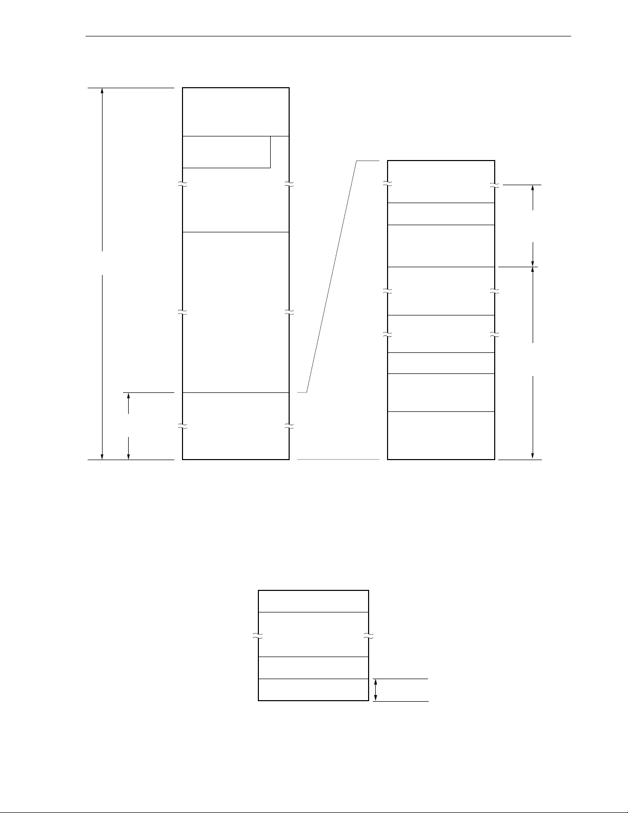
CHAPTER 3 CPU ARCHITECTURE
Figure 3-2. Memory Map (μPD78F0512)
FFFFH
Special function registers
FF00H
FEFFH
FEE0H
FEDFH
Internal high-speed RAM
FB00H
FAFFH
Data memory
space
6000H
5FFFH
Program
memory space
0000H
(SFR)
256 × 8 bits
General-purpose
registers
32 × 8 bits
1024 × 8 bits
Reserved
Flash memory
24576 × 8 bits
5FFFH
1085H
1084H
1080H
107FH
1000H
0FFFH
0800H
07FFH
0085H
0084H
0080H
007FH
0040H
003FH
0000H
Program area
Option byte area
5 x 8 bits
Program area
CALLF entry area
2048 x 8 bits
Program area
1915 x 8 bits
Option byte area
5 x 8 bits
CALLT table area
64 x 8 bits
Vector table area
64 x 8 bits
Note 1
Note 1
1FFFH
Boot cluster 1
Boot cluster 0
Notes 1. When boot swap is not used: Set the option bytes to 0080H to 0084H.
When boot swap is used: Set the option bytes to 0080H to 0084H and 1080H to 1084H.
2. Writing boot cluster 0 can be prohibited depending on the setting of security (see 25.8 Security
Setting).
Remark The flash memory is divided into blocks (one block = 1 KB). For the address values and block numbers,
see Table 3-2 Correspondence Between Address Values and Block Numbers in Flash Memory.
5FFFH
5C00H
5BFFH
Block 17H
Note 2
07FFH
0400H
03FFH
0000H
Block 01H
Block 00H
1 KB
User’s Manual U17336EJ5V0UD
49
Page 50
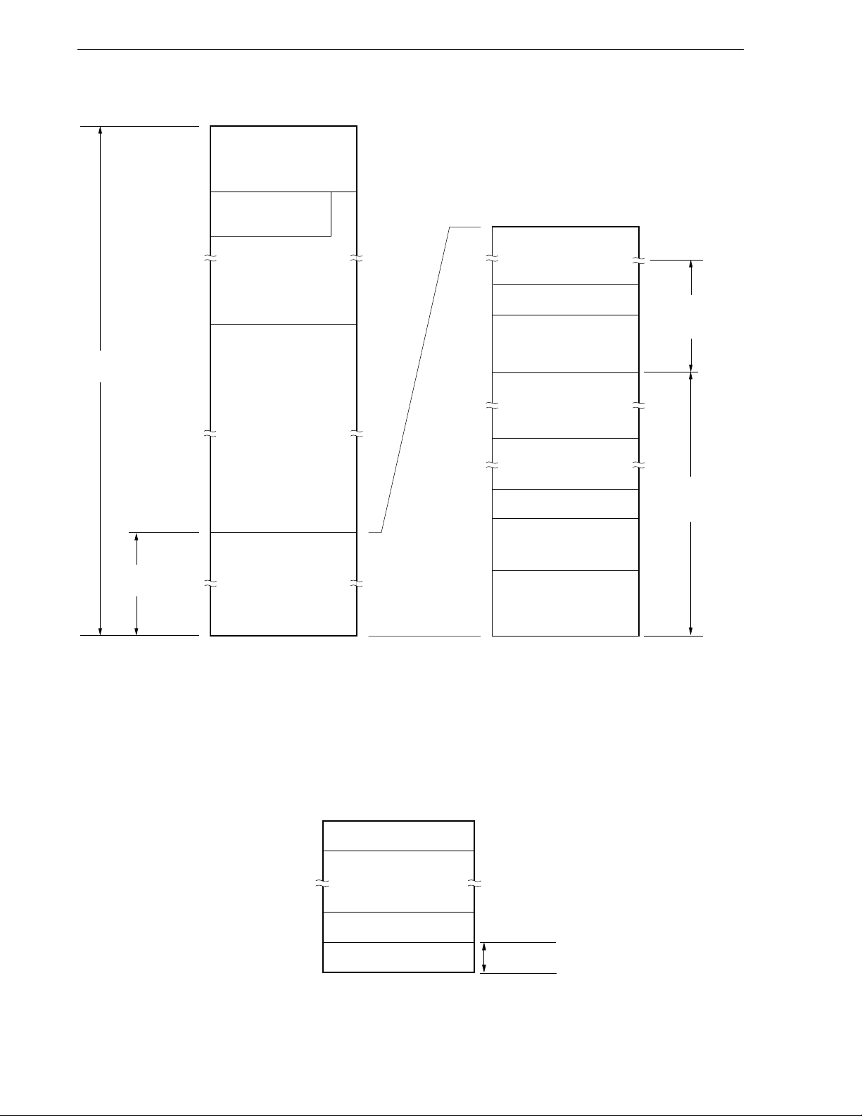
CHAPTER 3 CPU ARCHITECTURE
Figure 3-3. Memory Map (μPD78F0513)
FFFFH
Special function registers
FF00H
FEFFH
FEE0H
FEDFH
FB00H
FAFFH
Data memory
space
8000H
7FFFH
Program
memory space
0000H
(SFR)
256 × 8 bits
General-purpose
registers
32 × 8 bits
Internal high-speed RAM
1024 × 8 bits
Reserved
Flash memory
32768 × 8 bits
7FFFH
1085H
1084H
1080H
107FH
1000H
0FFFH
0800H
07FFH
0085H
0084H
0080H
007FH
0040H
003FH
0000H
Program area
Option byte area
5 x 8 bits
Program area
CALLF entry area
2048 x 8 bits
Program area
1915 x 8 bits
Option byte area
5 x 8 bits
CALLT table area
64 x 8 bits
Vector table area
64 x 8 bits
Note 1
Note 1
1FFFH
Boot cluster 1
Boot cluster 0
Notes 1. When boot swap is not used: Set the option bytes to 0080H to 0084H.
When boot swap is used: Set the option bytes to 0080H to 0084H and 1080H to 1084H.
2. Writing boot cluster 0 can be prohibited depending on the setting of security (see 25.8 Security
Setting).
Remark The flash memory is divided into blocks (one block = 1 KB). For the address values and block numbers,
see Table 3-2 Correspondence Between Address Values and Block Numbers in Flash Memory.
7FFFH
7C00H
7BFFH
Block 1FH
Note 2
50
07FFH
0400H
03FFH
0000H
Block 01H
Block 00H
1 KB
User’s Manual U17336EJ5V0UD
Page 51
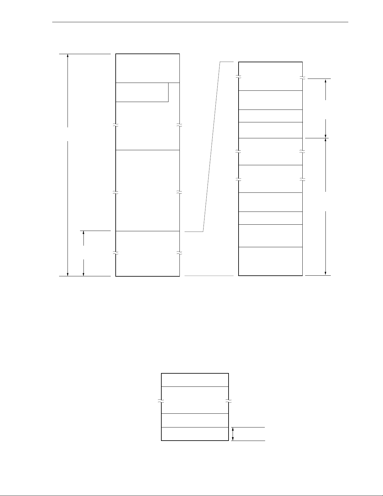
CHAPTER 3 CPU ARCHITECTURE
Figure 3-4. Memory Map (μPD78F0513D)
FFFFH
Data memory
space
Program
memory space
FF00H
FEFFH
FEE0H
FEDFH
FB00H
FAFFH
8000H
7FFFH
0000H
Special function registers
(SFR)
256 × 8 bits
General-purpose
registers
32 × 8 bits
Internal high-speed RAM
1024 × 8 bits
Reserved
Flash memory
32768 × 8 bits
7FFFH
108FH
108EH
1085H
1084H
1080H
107FH
1000H
0FFFH
0800H
07FFH
008FH
008EH
0085H
0084H
0080H
007FH
0040H
003FH
0000H
Program area
On-chip debug security
ID setting area
10 x 8 bits
Option byte area
5 x 8 bits
Program area
CALLF entry area
2048 x 8 bits
Program area
1905 x 8 bits
On-chip debug security
ID setting area
10 x 8 bits
Option byte area
5 x 8 bits
CALLT table area
64 x 8 bits
Vector table area
64 x 8 bits
Note 1
Note 1
Note 1
Note 1
1FFFH
Boot cluster 1
Boot cluster 0
Notes 1. When boot swap is not used: Set the option bytes to 0080H to 0084H, and the on-chip debug security
IDs to 0085H to 008EH.
When boot swap is used: Set the option bytes to 0080H to 0084H and 1080H to 1084H, and the
on-chip debug security IDs to 0085H to 008EH and 1085H to 108EH.
2. Writing boot cluster 0 can be prohibited depending on the setting of security (see 25.8 Security
Setting).
Remark The flash memory is divided into blocks (one block = 1 KB). For the address values and block numbers,
see Table 3-2 Correspondence Between Address Values and Block Numbers in Flash Memory.
7FFFH
7C00H
7BFFH
Block 1FH
Note 2
07FFH
0400H
03FFH
0000H
Block 01H
Block 00H
1 KB
User’s Manual U17336EJ5V0UD
51
Page 52
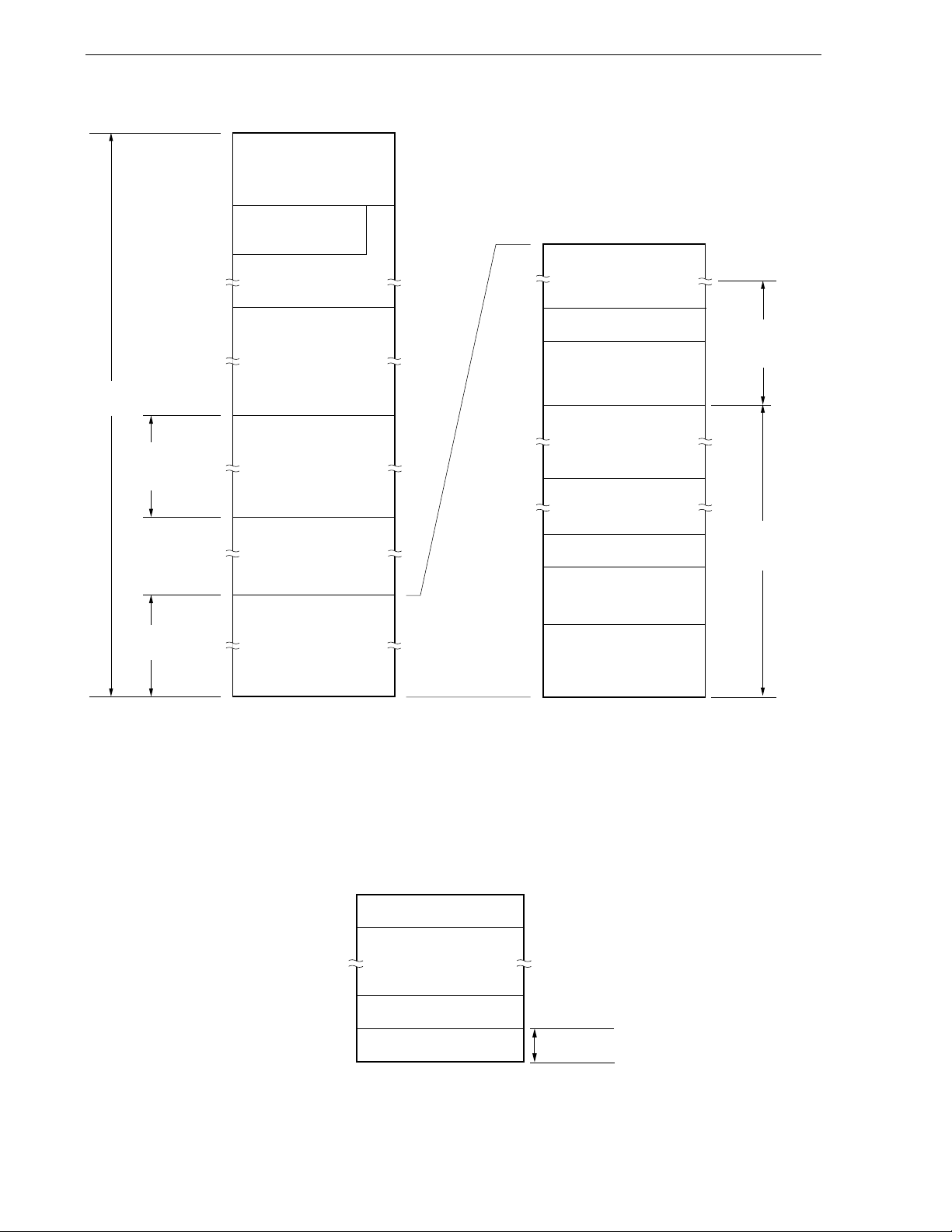
CHAPTER 3 CPU ARCHITECTURE
Figure 3-5. Memory Map (μPD78F0514)
FFFFH
Special function registers
(SFR)
256 × 8 bits
General-purpose
registers
32 × 8 bits
Internal high-speed RAM
1024 × 8 bits
Reserved
Internal expansion RAM
1024 × 8 bits
Reserved
Flash memory
49152 × 8 bits
BFFFH
1085H
1084H
1080H
107FH
1000H
0FFFH
0800H
07FFH
0085H
0084H
0080H
007FH
0040H
003FH
0000H
Program area
Option byte area
5 x 8 bits
Program area
CALLF entry area
2048 x 8 bits
Program area
1915 x 8 bits
Option byte area
5 x 8 bits
CALLT table area
64 x 8 bits
Vector table area
64 x 8 bits
Note 1
Note 1
1FFFH
Boot cluster 1
Boot cluster 0
Data memory
space
RAM space in
which instruction
can be fetched
Program
memory space
FF00H
FEFFH
FEE0H
FEDFH
FB00H
FAFFH
F800H
F7FFH
F400H
F3FFH
C000H
BFFFH
0000H
Notes 1. When boot swap is not used: Set the option bytes to 0080H to 0084H.
When boot swap is used: Set the option bytes to 0080H to 0084H and 1080H to 1084H.
2. Writing boot cluster 0 can be prohibited depending on the setting of security (see 25.8 Security
Setting).
Remark The flash memory is divided into blocks (one block = 1 KB). For the address values and block numbers,
see Table 3-2 Correspondence Between Address Values and Block Numbers in Flash Memory.
BFFFH
BC00H
BBFFH
Block 2FH
Note 2
52
07FFH
0400H
03FFH
0000H
Block 01H
Block 00H
1 KB
User’s Manual U17336EJ5V0UD
Page 53
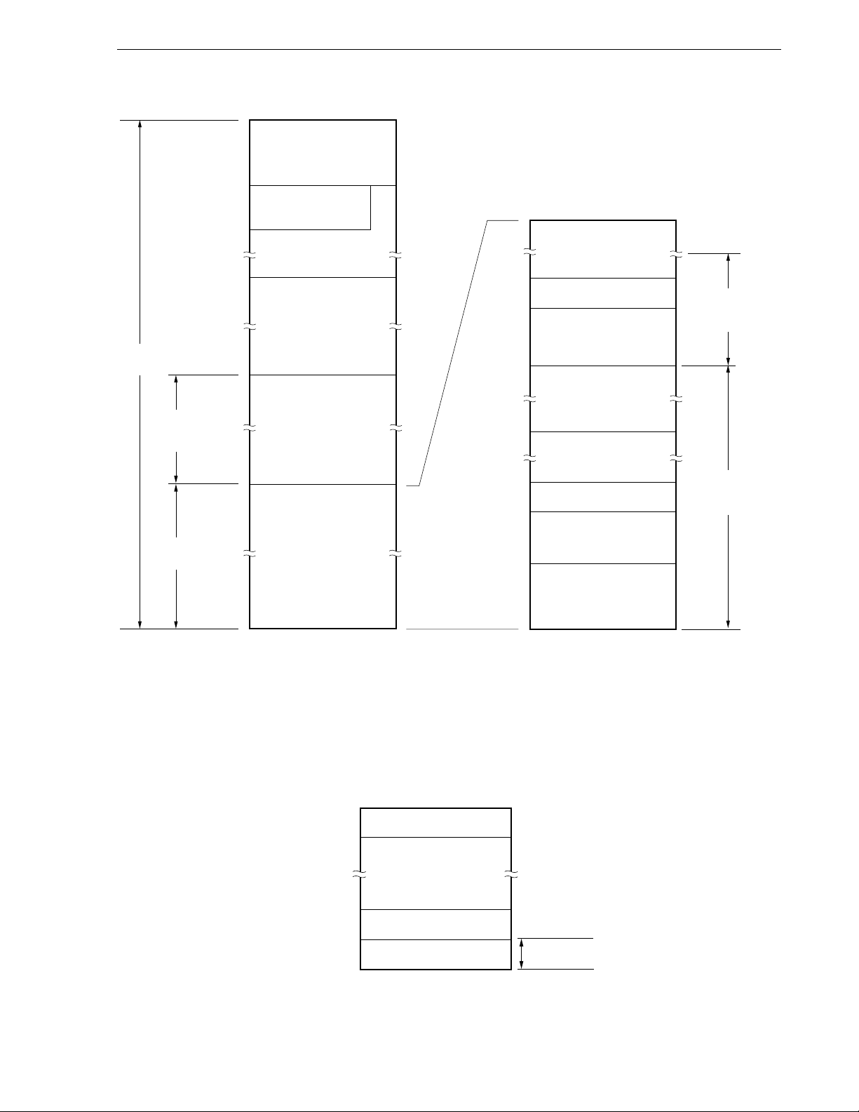
CHAPTER 3 CPU ARCHITECTURE
Figure 3-6. Memory Map (μPD78F0515)
FFFFH
Data memory
space
RAM space in
which instruction
can be fetched
Program
memory space
Special function registers
FF00H
FEFFH
FEE0H
FEDFH
FB00H
FAFFH
F800H
F7FFH
F000H
EFFFH
0000H
(SFR)
256 × 8 bits
General-purpose
registers
32 × 8 bits
Internal high-speed RAM
1024 × 8 bits
Reserved
Internal expansion RAM
2048 × 8 bits
Flash memory
61440 × 8 bits
EFFFH
1085H
1084H
1080H
107FH
1000H
0FFFH
0800H
07FFH
0085H
0084H
0080H
007FH
0040H
003FH
0000H
Program area
Option byte area
5 x 8 bits
Program area
CALLF entry area
2048 x 8 bits
Program area
1915 x 8 bits
Option byte area
5 x 8 bits
CALLT table area
64 x 8 bits
Vector table area
64 x 8 bits
Note 1
Note 1
1FFFH
Boot cluster 1
Boot cluster 0
Notes 1. When boot swap is not used: Set the option bytes to 0080H to 0084H.
When boot swap is used: Set the option bytes to 0080H to 0084H and 1080H to 1084H.
2. Writing boot cluster 0 can be prohibited depending on the setting of security (see 25.8 Security
Setting).
Remark The flash memory is divided into blocks (one block = 1 KB). For the address values and block numbers,
see Table 3-2 Correspondence Between Address Values and Block Numbers in Flash Memory.
EFFFH
EC00H
EBFFH
Block 3BH
Note 2
07FFH
0400H
03FFH
0000H
Block 01H
Block 00H
1 KB
User’s Manual U17336EJ5V0UD
53
Page 54
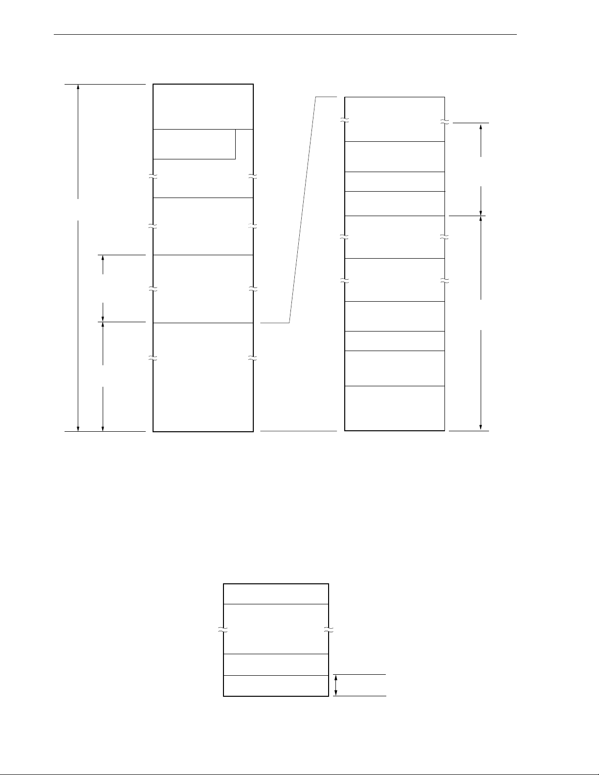
CHAPTER 3 CPU ARCHITECTURE
Figure 3-7. Memory Map (μPD78F0515D)
FFFFH
Data memory
space
RAM space in
which instruction
can be fetched
Program
memory space
FF00H
FEFFH
FEE0H
FEDFH
FB00H
FAFFH
F800H
F7FFH
F000H
EFFFH
0000H
Special function registers
(SFR)
256 × 8 bits
General-purpose
registers
32 × 8 bits
Internal high-speed RAM
1024 × 8 bits
Reserved
Internal expansion RAM
2048 × 8 bits
Flash memory
61440 × 8 bits
EFFFH
108FH
108EH
1085H
1084H
1080H
107FH
1000H
0FFFH
0800H
07FFH
008FH
008EH
0085H
0084H
0080H
007FH
0040H
003FH
0000H
Program area
On-chip debug security
ID setting area
10 x 8 bits
Option byte area
5 x 8 bits
Program area
CALLF entry area
2048 x 8 bits
Program area
1905 x 8 bits
On-chip debug security
ID setting area
10 x 8 bits
Option byte area
5 x 8 bits
CALLT table area
64 x 8 bits
Vector table area
64 x 8 bits
Note 1
Note 1
Note1
Note 1
1FFFH
Boot cluster 1
Boot cluster 0
Notes 1. When boot swap is not used: Set the option bytes to 0080H to 0084H, and the on-chip debug security
IDs to 0085H to 008EH.
When boot swap is used: Set the option bytes to 0080H to 0084H and 1080H to 1084H, and the
on-chip debug security IDs to 0085H to 008EH and 1085H to 108EH.
2. Writing boot cluster 0 can be prohibited depending on the setting of security (see 25.8 Security
Setting).
Remark The flash memory is divided into blocks (one block = 1 KB). For the address values and block numbers,
see Table 3-2 Correspondence Between Address Values and Block Numbers in Flash Memory.
EFFFH
EC00H
EBFFH
Block 3BH
Note 2
54
07FFH
0400H
03FFH
0000H
Block 01H
Block 00H
User’s Manual U17336EJ5V0UD
1 KB
Page 55
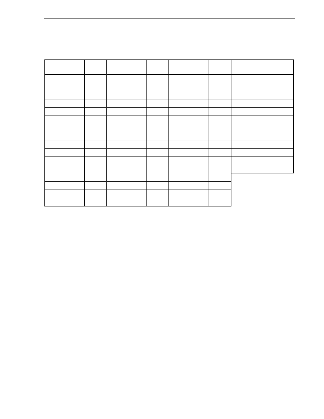
CHAPTER 3 CPU ARCHITECTURE
Correspondence between the address values and block numbers in the flash memory are shown below.
Table 3-2. Correspondence Between Address Values and Block Numbers in Flash Memory
Address Value
0000H to 03FFH 00H 4000H to 43FFH 10H 8000H to 83FFH 20H C000H to C3FFH 30H
0400H to 07FFH 01H 4400H to 47FFH 11H 8400H to 87FFH 21H C400H to C7FFH 31H
0800H to 0BFFH 02H 4800H to 4BFFH 12H 8800H to 8BFFH 22H C800H to CBFFH 32H
0C00H to 0FFFH 03H 4C00H to 4FFFH 13H 8C00H to 8FFFH 23H CC00H to CFFFH 33H
1000H to 13FFH 04H 5000H to 53FFH 14H 9000H to 93FFH 24H D000H to D3FFH 34H
1400H to 17FFH 05H 5400H to 57FFH 15H 9400H to 97FFH 25H D400H to D7FFH 35H
1800H to 1BFFH 06H 5800H to 5BFFH 16H 9800H to 9BFFH 26H D800H to DBFFH 36H
1C00H to 1FFFH 07H 5C00H to 5FFFH 17H 9C00H to 9FFFH 27H DC00H to DFFFH 37H
2000H to 23FFH 08H 6000H to 63FFH 18H A000H to A3FFH 28H E000H to E3FFH 38H
2400H to 27FFH 09H 6400H to 67FFH 19H A400H to A7FFH 29H E400H to E7FFH 39H
2800H to 2BFFH 0AH 6800H to 6BFFH 1AH A800H to ABFFH 2AH E800H to EBFFH 3AH
2C00H to 2FFFH 0BH 6C00H to 6FFFH 1BH AC00H to AFFFH 2BH EC00H to EFFFH 3BH
3000H to 33FFH 0CH 7000H to 73FFH 1CH B000H to B3FFH 2CH
3400H to 37FFH 0DH 7400H to 77FFH 1DH B400H to B7FFH 2DH
3800H to 3BFFH 0EH 7800H to 7BFFH 1EH B800H to BBFFH 2EH
3C00H to 3FFFH 0FH 7C00H to 7FFFH 1FH BC00H to BFFFH 2FH
Block
Number
Address Value
Block
Number
Address Value
Block
Number
Address Value
Remark
μ
PD78F0511: Block numbers 00H to 0FH
μ
PD78F0512: Block numbers 00H to 17H
μ
PD78F0513, 78F0513D: Block numbers 00H to 1FH
μ
PD78F0514: Block numbers 00H to 2FH
μ
PD78F0515, 78F0515D: Block numbers 00H to 3BH
Block
Number
User’s Manual U17336EJ5V0UD
55
Page 56
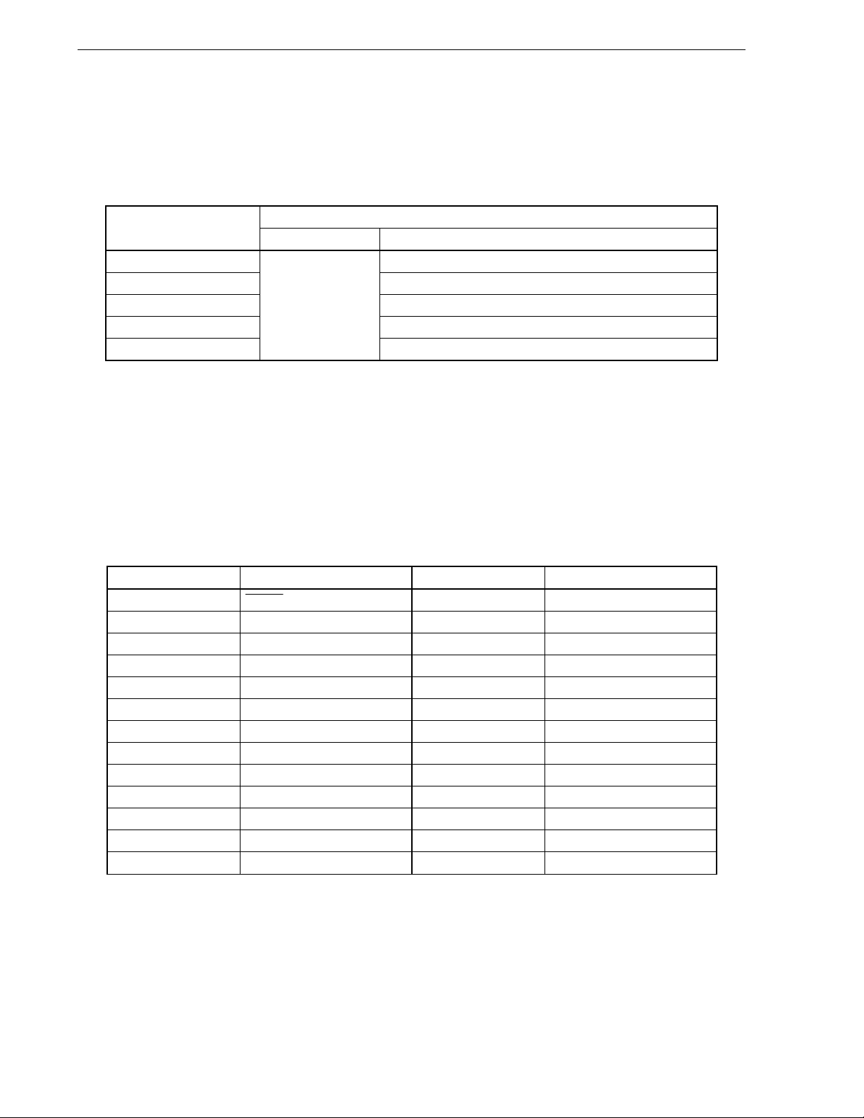
CHAPTER 3 CPU ARCHITECTURE
3.1.1 Internal program memory space
The internal program memory space stores the program and table data. Normally, it is addressed with the program
counter (PC).
78K0/KC2 products incorporate internal ROM (flash memory), as shown below.
Table 3-3. Internal ROM Capacity
Internal ROM Part Number
Structure Capacity
μ
PD78F0511 16384 × 8 bits (0000H to 3FFFH)
μ
PD78F0512 24576 × 8 bits (0000H to 5FFFH)
μ
PD78F0513, 78F0513D 32768 × 8 bits (0000H to 7FFFH)
μ
PD78F0514 49152 × 8 bits (0000H to BFFFH)
μ
PD78F0515, 78F0515D
Flash memory
61440 × 8 bits (0000H to EFFFH)
The internal program memory space is divided into the following areas.
(1) Vector table area
The 64-byte area 0000H to 003FH is reserved as a vector table area. The program start addresses for branch
upon reset or generation of each interrupt request are stored in the vector table area.
Of the 16-bit address, the lower 8 bits are stored at even addresses and the higher 8 bits are stored at odd
addresses.
Table 3-4. Vector Table
Vector Table Address Interrupt Source Vector Table Address Interrupt Source
0000H RESET input, POC, LVI, WDT 001CH INTTMH0
0004H INTLVI 001EH INTTM50
0006H INTP0 0020H INTTM000
0008H INTP1 0022H INTTM010
000AH INTP2 0024H INTAD
000CH INTP3 0026H INTSR0
000EH INTP4 0028H INTWTI
0010H INTP5 002AH INTTM51
0012H INTSRE6 002CH INTKR
0014H INTSR6 002EH INTWT
0016H INTST6 0030H INTP6
0018H INTCSI10/INTST0 0034H INTIIC0/INTDMU
001AH INTTMH1 003EH BRK
Note 1
Notes 1. Available only in the 48-pin products.
2. Available only in the
μ
PD78F0514, 78F0515, and 78F0515D.
Note 2
56
User’s Manual U17336EJ5V0UD
Page 57

CHAPTER 3 CPU ARCHITECTURE
(2) CALLT instruction table area
The 64-byte area 0040H to 007FH can store the subroutine entry address of a 1-byte call instruction (CALLT).
(3) Option byte area
A 5-byte area of 0080H to 0084H and 1080H to 1084H can be used as an option byte area. Set the option byte
at 0080H to 0084H when the boot swap is not used, and at 0080H to 0084H and 1080H to 1084H when the boot
swap is used. For details, see CHAPTER 24 OPTION BYTE.
(4) CALLF instruction entry area
The area 0800H to 0FFFH can perform a direct subroutine call with a 2-byte call instruction (CALLF).
(5) On-chip debug security ID setting area (
μ
PD78F0513D and 78F0515D only)
A 10-byte area of 0085H to 008EH and 1085H to 108EH can be used as an on-chip debug security ID setting
area. Set the on-chip debug security ID of 10 bytes at 0085H to 008EH when the boot swap is not used and at
0085H to 008EH and 1085H to 108EH when the boot swap is used. For details, see CHAPTER 26 ON-CHIP
DEBUG FUNCTION (
μ
PD78F0513D AND 78F0515D ONLY).
User’s Manual U17336EJ5V0UD
57
Page 58
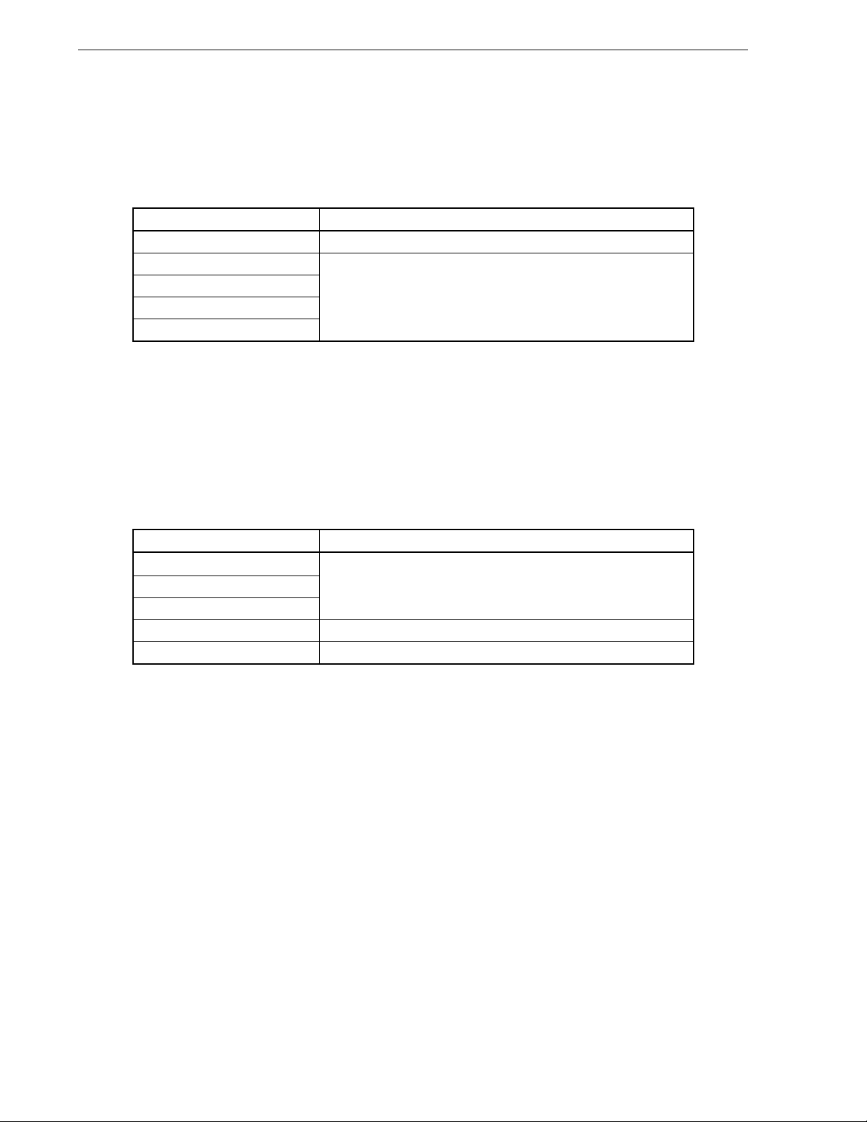
CHAPTER 3 CPU ARCHITECTURE
3.1.2 Internal data memory space
78K0/KC2 products incorporate the following RAMs.
(1) Internal high-speed RAM
Table 3-5. Internal High-Speed RAM Capacity
Part Number Internal High-Speed RAM
μ
PD78F0511 768 × 8 bits (FC00H to FEFFH)
μ
PD78F0512
μ
PD78F0513, 78F0513D
μ
PD78F0514
μ
PD78F0515, 78F0515D
1024 × 8 bits (FB00H to FEFFH)
The 32-byte area FEE0H to FEFFH is assigned to four general-purpose register banks consisting of eight 8-bit
registers per bank.
This area cannot be used as a program area in which instructions are written and executed.
The internal high-speed RAM can also be used as a stack memory.
(2) Internal expansion RAM
Table 3-6. Internal Expansion RAM Capacity
Part Number Internal Expansion RAM
μ
PD78F0511
μ
PD78F0512
μ
PD78F0513, 78F0513D
μ
PD78F0514 1024 × 8 bits (F400H to F7FFH)
μ
PD78F0515, 78F0515D 2048 × 8 bits (F000H to F7FFH)
−
The internal expansion RAM can also be used as a normal data area similar to the internal high-speed RAM, as
well as a program area in which instructions can be written and executed.
The internal expansion RAM cannot be used as a stack memory.
58
User’s Manual U17336EJ5V0UD
Page 59

CHAPTER 3 CPU ARCHITECTURE
3.1.3 Special function register (SFR) area
On-chip peripheral hardware special function registers (SFRs) are allocated in the area FF00H to FFFFH (see
Table 3-7 Special Function Register List in 3.2.3 Special function registers (SFRs)).
Caution Do not access addresses to which SFRs are not assigned.
3.1.4 Data memory addressing
Addressing refers to the method of specifying the address of the instruction to be executed next or the address of
the register or memory relevant to the execution of instructions.
Several addressing modes are provided for addressing the memory relevant to the execution of instructions for the
78K0/KC2, based on operability and other considerations. For areas containing data memory in particular, special
addressing methods designed for the functions of special function registers (SFR) and general-purpose registers are
available for use. Figures 3-8 to 3-14 show correspondence between data memory and addressing. For details of
each addressing mode, see 3.4 Operand Address Addressing.
User’s Manual U17336EJ5V0UD
59
Page 60
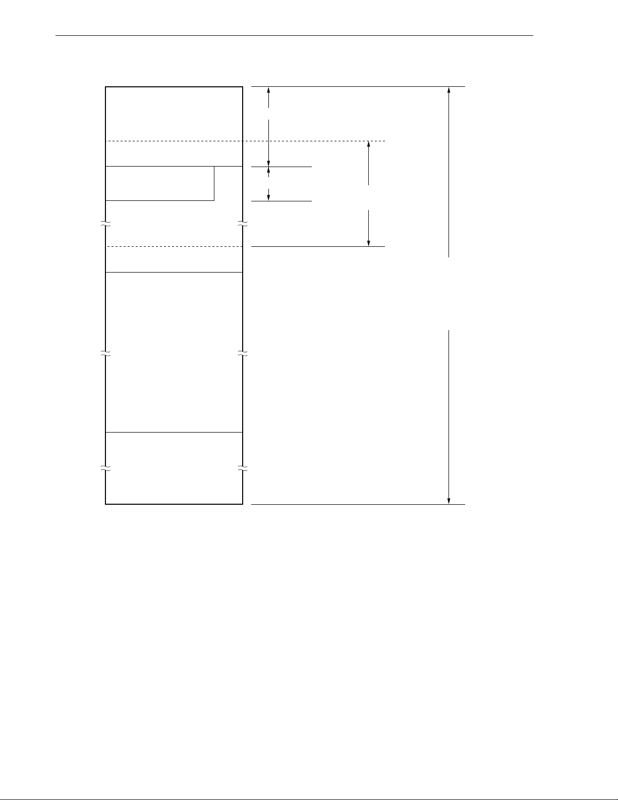
FFFFH
CHAPTER 3 CPU ARCHITECTURE
Figure 3-8. Correspondence Between Data Memory and Addressing (μPD78F0511)
FF20H
FF1FH
FF00H
FEFFH
FEE0H
FEDFH
FE20H
FE1FH
FC00H
FBFFH
Special function registers (SFR)
256 × 8 bits
General-purpose registers
32 × 8 bits
Internal high-speed RAM
768 × 8 bits
Reserved
SFR addressing
Register addressing
Short direct
addressing
Direct addressing
Register indirect addressing
Based addressing
Based indexed addressing
4000H
3FFFH
0000H
Flash memory
16384 × 8 bits
60
User’s Manual U17336EJ5V0UD
Page 61
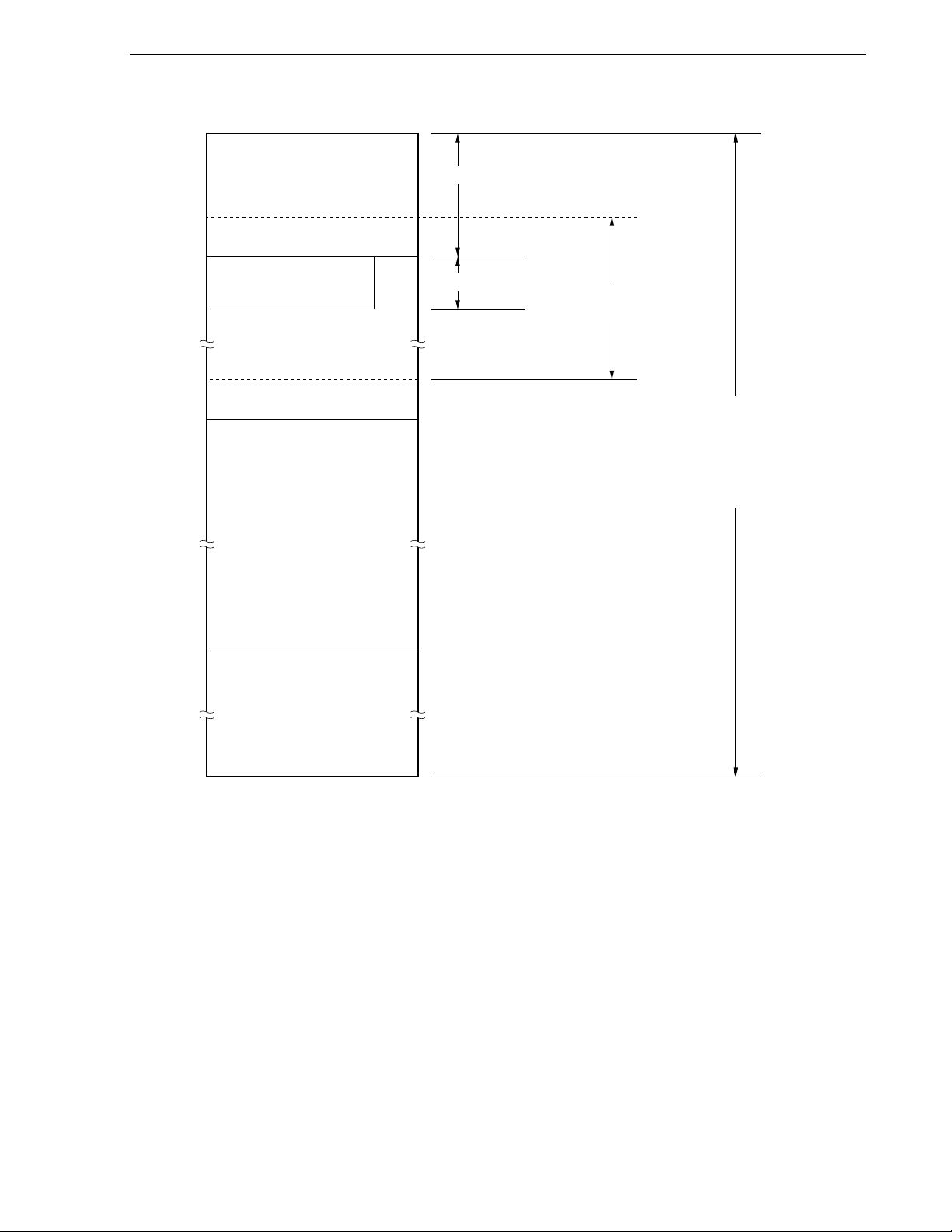
FFFFH
CHAPTER 3 CPU ARCHITECTURE
Figure 3-9. Correspondence Between Data Memory and Addressing (μPD78F0512)
FF20H
FF1FH
FF00H
FEFFH
FEE0H
FEDFH
FE20H
FE1FH
FB00H
FAFFH
Special function registers (SFR)
256 × 8 bits
General-purpose registers
32 × 8 bits
Internal high-speed RAM
1024 × 8 bits
Reserved
SFR addressing
Register addressing
Short direct
addressing
Direct addressing
Register indirect addressing
Based addressing
Based indexed addressing
6000H
5FFFH
0000H
Flash memory
24576 × 8 bits
User’s Manual U17336EJ5V0UD
61
Page 62
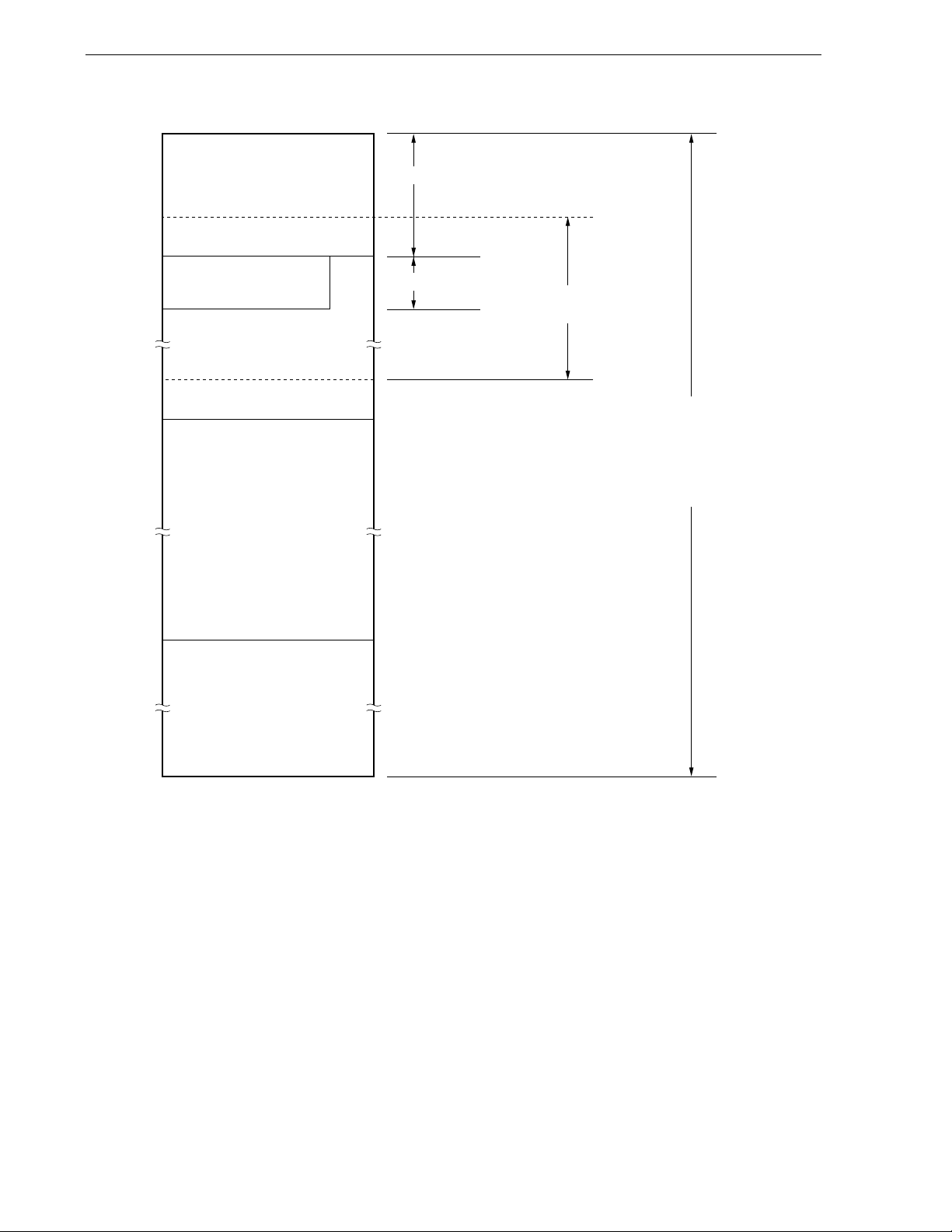
CHAPTER 3 CPU ARCHITECTURE
Figure 3-10. Correspondence Between Data Memory and Addressing (μPD78F0513 and 78F0513D)
FFFFH
FF20H
FF1FH
FF00H
FEFFH
FEE0H
FEDFH
FE20H
FE1FH
FB00H
FAFFH
Special function registers (SFR)
256 × 8 bits
General-purpose registers
32 × 8 bits
Internal high-speed RAM
1024 × 8 bits
Reserved
SFR addressing
Register addressing
Short direct
addressing
Direct addressing
Register indirect addressing
Based addressing
Based indexed addressing
8000H
7FFFH
0000H
Flash memory
32768 × 8 bits
62
User’s Manual U17336EJ5V0UD
Page 63
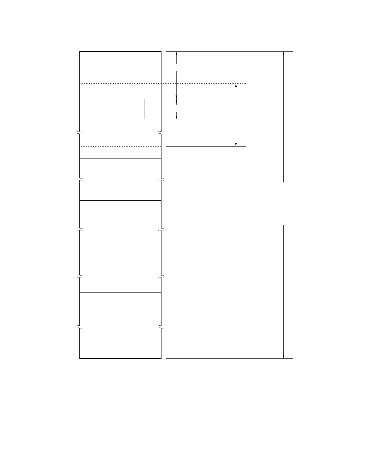
CHAPTER 3 CPU ARCHITECTURE
Figure 3-11 . Correspondence Between Data Memory and Addressing (μPD78F0514)
FFFFH
FF20H
FF1FH
FF00H
FEFFH
FEE0H
FEDFH
FE20H
FE1FH
FB00H
FAFFH
F800H
F7FFH
Special function registers (SFR)
256 × 8 bits
General-purpose registers
32 × 8 bits
Internal high-speed RAM
1024 × 8 bits
Reserved
Internal expansion RAM
1024 × 8 bits
SFR addressing
Register addressing
Short direct
addressing
Direct addressing
Register indirect addressing
Based addressing
Based indexed addressing
F400H
F3FFH
C000H
BFFFH
0000H
Reserved
Flash memory
49152 × 8 bits
User’s Manual U17336EJ5V0UD
63
Page 64
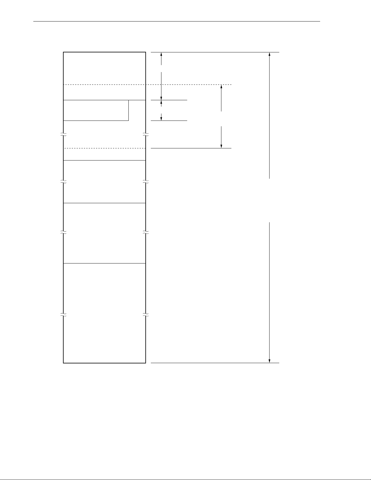
CHAPTER 3 CPU ARCHITECTURE
Figure 3-12. Correspondence Between Data Memory and Addressing (μPD78F0515 and 78F0515D)
FFFFH
FF20H
FF1FH
FF00H
FEFFH
FEE0H
FEDFH
FE20H
FE1FH
FB00H
FAFFH
F800H
F7FFH
Special function registers (SFR)
256 × 8 bits
General-purpose registers
32 × 8 bits
Internal high-speed RAM
1024 × 8 bits
Reserved
Internal expansion RAM
2048 × 8 bits
SFR addressing
Register addressing
Short direct
addressing
Direct addressing
Register indirect addressing
Based addressing
Based indexed addressing
F000H
EFFFH
0000H
Flash memory
61440 × 8 bits
64
User’s Manual U17336EJ5V0UD
Page 65
CHAPTER 3 CPU ARCHITECTURE
3.2 Processor Registers
The 78K0/KC2 products incorporate the following processor registers.
3.2.1 Control registers
The control registers control the program sequence, statuses and stack memory. The control registers consist of a
program counter (PC), a program status word (PSW) and a stack pointer (SP).
(1) Program counter (PC)
The program counter is a 16-bit register that holds the address information of the next program to be executed.
In normal operation, PC is automatically incremented according to the number of bytes of the instruction to be
fetched. When a branch instruction is executed, immediate data and register contents are set.
Reset signal generation sets the reset vector table values at addresses 0000H and 0001H to the program counter.
Figure 3-13. Format of Program Counter
15
PC15 PC14 PC13 PC12 PC11 PC10
PC
PC9 PC8 PC7 PC6 PC5 PC4 PC3 PC2 PC1 PC0
(2) Program status word (PSW)
The program status word is an 8-bit register consisting of various flags set/reset by instruction execution.
Program status word contents are stored in the stack area upon interrupt request generation or PUSH PSW
instruction execution and are restored upon execution of the RETB, RETI and POP PSW instructions.
Reset signal generation sets PSW to 02H.
Figure 3-14. Format of Program Status Word
70
IE Z RBS1 AC RBS0 ISP CY
0PSW
(a) Interrupt enable flag (IE)
This flag controls the interrupt request acknowledge operations of the CPU.
When 0, the IE flag is set to the interrupt disabled (DI) state, and all maskable interrupt requests are disabled.
When 1, the IE flag is set to the interrupt enabled (EI) state and interrupt request acknowledgment is
controlled with an in-service priority flag (ISP), an interrupt mask flag for various interrupt sources, and a
priority specification flag.
The IE flag is reset (0) upon DI instruction execution or interrupt acknowledgment and is set (1) upon EI
instruction execution.
0
User’s Manual U17336EJ5V0UD
65
Page 66

CHAPTER 3 CPU ARCHITECTURE
Page 67
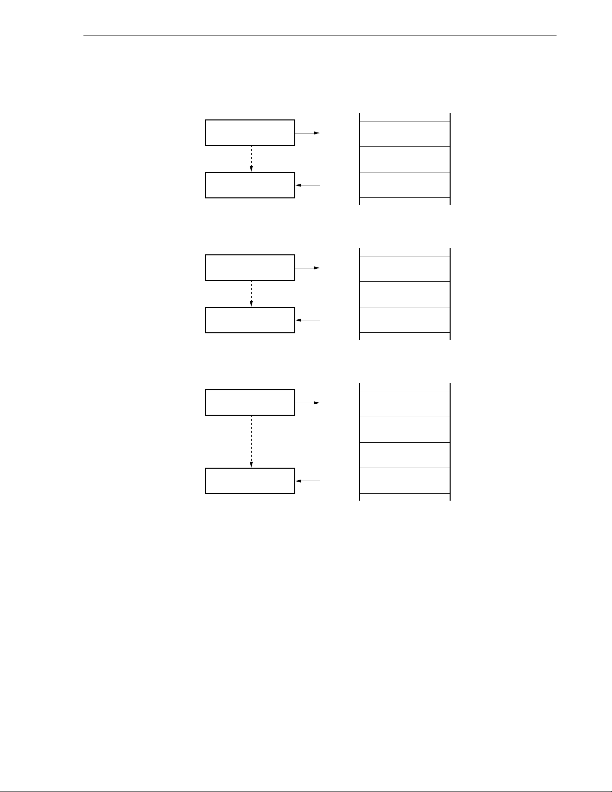
CHAPTER 3 CPU ARCHITECTURE
Figure 3-16. Data to Be Saved to Stack Memory
(a) PUSH rp instruction (when SP = FEE0H)
SP
SP
FEE0H
FEDEH
FEE0H
FEDFH
FEDEH
Register pair higher
Register pair lower
(b) CALL, CALLF, CALLT instructions (when SP = FEE0H)
SP
SP
FEE0H
FEDEH
FEE0H
FEDFH
FEDEH
PC15 to PC8
PC7 to PC0
(c) Interrupt, BRK instructions (when SP = FEE0H)
SP
FEE0H
FEE0H
SP
FEDDH
FEDFH
FEDEH
FEDDH
PSW
PC15 to PC8
PC7 to PC0
User’s Manual U17336EJ5V0UD
67
Page 68
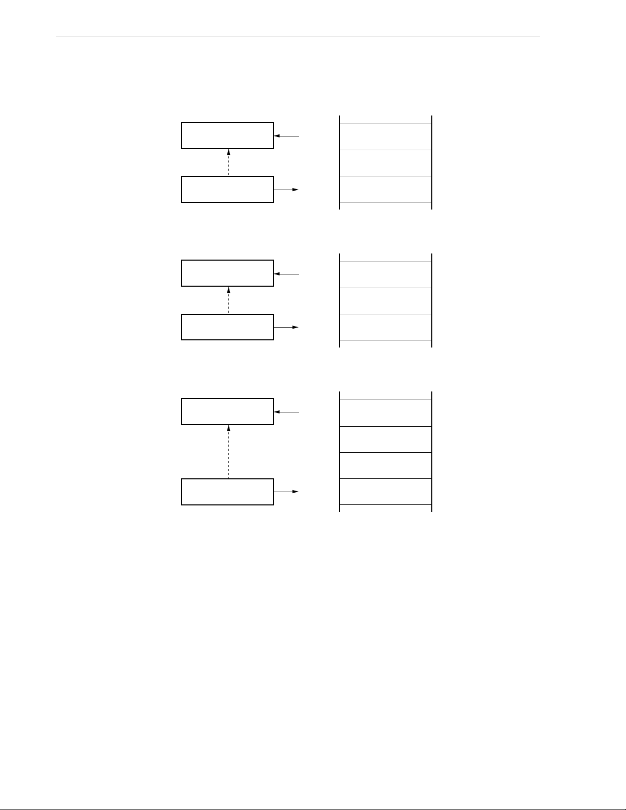
CHAPTER 3 CPU ARCHITECTURE
Figure 3-17. Data to Be Restored from Stack Memory
(a) POP rp instruction (when SP = FEDEH)
SP
SP
FEE0H
FEDEH
FEE0H
FEDFH
FEDEH
Register pair higher
Register pair lower
(b) RET instruction (when SP = FEDEH)
SP
SP
FEE0H
FEDEH
FEE0H
FEDFH
FEDEH
PC15 to PC8
PC7 to PC0
(c) RETI, RETB instructions (when SP = FEDDH)
SP
FEE0H
FEE0H
SP
FEDDH
FEDFH
FEDEH
FEDDH
PSW
PC15 to PC8
PC7 to PC0
68
User’s Manual U17336EJ5V0UD
Page 69
CHAPTER 3 CPU ARCHITECTURE
3.2.2 General-purpose registers
General-purpose registers are mapped at particular addresses (FEE0H to FEFFH) of the data memory. The
general-purpose registers consists of 4 banks, each bank consisting of eight 8-bit registers (X, A, C, B, E, D, L, and H).
Each register can be used as an 8-bit register, and two 8-bit registers can also be used in a pair as a 16-bit register
(AX, BC, DE, and HL).
These registers can be described in terms of function names (X, A, C, B, E, D, L, H, AX, BC, DE, and HL) and
absolute names (R0 to R7 and RP0 to RP3).
Register banks to be used for instruction execution are set by the CPU control instruction (SEL RBn). Because of
the 4-register bank configuration, an efficient program can be created by switching between a register for normal
processing and a register for interrupts for each bank.
Figure 3-18. Configuration of General-Purpose Registers
(a) Function name
16-bit processing 8-bit processing
FEFFH
FEF8H
FEF0H
FEE8H
FEE0H
Register bank 0
Register bank 1
Register bank 2
Register bank 3
HL
DE
BC
AX
15 0 7 0
H
L
D
E
B
C
A
X
(b) Absolute name
16-bit processing 8-bit processing
FEFFH
FEF8H
FEF0H
FEE8H
FEE0H
Register bank 0
Register bank 1
Register bank 2
Register bank 3
RP3
RP2
RP1
RP0
15 0 7 0
R7
R6
R5
R4
R3
R2
R1
R0
User’s Manual U17336EJ5V0UD
69
Page 70

CHAPTER 3 CPU ARCHITECTURE
3.2.3 Special function registers (SFRs)
Unlike a general-purpose register, each special function register has a special function.
SFRs are allocated to the FF00H to FFFFH area.
Special function registers can be manipulated like general-purpose registers, using operation, transfer, and bit
manipulation instructions. The manipulatable bit units, 1, 8, and 16, depend on the special function register type.
Each manipulation bit unit can be specified as follows.
• 1-bit manipulation
Describe the symbol reserved by the assembler for the 1-bit manipulation instruction operand (sfr.bit).
This manipulation can also be specified with an address.
• 8-bit manipulation
Describe the symbol reserved by the assembler for the 8-bit manipulation instruction operand (sfr).
This manipulation can also be specified with an address.
• 16-bit manipulation
Describe the symbol reserved by the assembler for the 16-bit manipulation instruction operand (sfrp).
When specifying an address, describe an even address.
Table 3-7 gives a list of the special function registers. The meanings of items in the table are as follows.
• Symbol
Symbol indicating the address of a special function register. It is a reserved word in the RA78K0, and is defined
as an sfr variable using the #pragma sfr directive in the CC78K0. When using the RA78K0, ID78K0-QB, and
SM+ for 78K0/KX2, symbols can be written as an instruction operand.
• R/W
Indicates whether the corresponding special function register can be read or written.
R/W: Read/write enable
R: Read only
W: Write only
• Manipulatable bit units
Indicates the manipulatable bit unit (1, 8, or 16). “−” indicates a bit unit for which manipulation is not possible.
• After reset
Indicates each register status upon reset signal generation.
70
User’s Manual U17336EJ5V0UD
Page 71
CHAPTER 3 CPU ARCHITECTURE
Table 3-7. Special Function Register List (1/4)
FF00H Port register 0 P0 R/W
FF01H Port register 1 P1 R/W
FF02H Port register 2 P2 R/W
FF03H Port register 3 P3 R/W
FF04H Port register 4 P4 R/W
FF06H Port register 6 P6 R/W
FF07H Port register 7 P7 R/W
FF08H 10-bit A/D conversion result register ADCR R
FF09H 8-bit A/D conversion result register ADCRH R
FF0AH Receive buffer register 6 RXB6 R
FF0BH Transmit buffer register 6 TXB6 R/W
FF0CH Port register 12 P12 R/W
FF0DH Port register 13
FF0EH Port register 14
Note
P13 R/W
Note
P14 R/W
FF0FH Serial I/O shift register 10 SIO10 R
FF10H
16-bit timer counter 00 TM00 R
FF11H
FF12H
16-bit timer capture/compare register 000 CR000 R/W
FF13H
FF14H
16-bit timer capture/compare register 010 CR010 R/W
FF15H
FF16H 8-bit timer counter 50 TM50 R
FF17H 8-bit timer compare register 50 CR50 R/W
FF18H 8-bit timer H compare register 00 CMP00 R/W
FF19H 8-bit timer H compare register 10 CMP10 R/W
FF1AH 8-bit timer H compare register 01 CMP01 R/W
FF1BH 8-bit timer H compare register 11 CMP11 R/W
FF1FH 8-bit timer counter 51 TM51 R
FF20H Port mode register 0 PM0 R/W
FF21H Port mode register 1 PM1 R/W
FF22H Port mode register 2 PM2 R/W
FF23H Port mode register 3 PM3 R/W
FF24H Port mode register 4 PM4 R/W
FF26H Port mode register 6 PM6 R/W
FF27H Port mode register 7 PM7 R/W
FF28H A/D converter mode register ADM R/W
FF29H Analog input channel specification register ADS R/W
FF2CH Port mode register 12 PM12 R/W
FF2EH Port mode register 14
Note
PM14 R/W
FF2FH A/D port configuration register ADPC R/W
Note Available only in the 48-pin products.
Manipulatable Bit Unit Address Special Function Register (SFR) Name Symbol R/W
1 Bit 8 Bits 16 Bits
√ √ −
√ √ −
√ √ −
√ √ −
√ √ −
√ √ −
√ √ −
− − √
− √ −
− √ −
− √ −
√ √ −
√ √ −
√ √ −
− √ −
− − √
− − √
− − √
− √ −
− √ −
− √ −
− √ −
− √ −
− √ −
− √ −
√ √ −
√ √ −
√ √ −
√ √ −
√ √ −
√ √ −
√ √ −
√ √ −
√ √ −
√ √ −
√ √ −
√ √ −
After
Reset
00H
00H
00H
00H
00H
00H
00H
0000H
00H
FFH
FFH
00H
00H
00H
00H
0000H
0000H
0000H
00H
00H
00H
00H
00H
00H
00H
FFH
FFH
FFH
FFH
FFH
FFH
FFH
00H
00H
FFH
FFH
00H
User’s Manual U17336EJ5V0UD
71
Page 72
CHAPTER 3 CPU ARCHITECTURE
Table 3-7. Special Function Register List (2/4)
FF30H Pull-up resistor option register 0 PU0 R/W
FF31H Pull-up resistor option register 1 PU1 R/W
FF33H Pull-up resistor option register 3 PU3 R/W
FF34H Pull-up resistor option register 4 PU4 R/W
FF37H Pull-up resistor option register 7 PU7 R/W
FF3CH Pull-up resistor option register 12 PU12 R/W
FF3EH Pull-up resistor option register 14
FF40H Clock output selection register
Note 1
PU14 R/W
Note 1
CKS R/W
FF41H 8-bit timer compare register 51 CR51 R/W
FF43H 8-bit timer mode control register 51 TMC51 R/W
FF48H External interrupt rising edge enable register EGP R/W
FF49H External interrupt falling edge enable register EGN R/W
FF4FH Input switch control register ISC R/W
FF50H Asynchronous serial interface operation mode
ASIM6 R/W
register 6
FF53H Asynchronous serial interface reception error
ASIS6 R
status register 6
FF55H Asynchronous serial interface transmission
ASIF6 R
status register 6
FF56H Clock selection register 6 CKSR6 R/W
FF57H Baud rate generator control register 6 BRGC6 R/W
FF58H Asynchronous serial interface control register 6 ASICL6 R/W
FF60H
Remainder data register 0
FF61H
FF62H
Multiplication/division data register A0
FF63H
FF64H
FF65H
FF66H
Multiplication/division data register B0
FF67H
FF68H Multiplier/divider control register 0
Note 2
Note 2
Note 2
Note 2
DMUC0 R/W
SDR0
MDA0L
MDA0H
MDB0
SDR0L
SDR0H
MDA0LL
MDA0LH
MDA0HL
MDA0HH
MDB0L
MDB0H
R/W
R/W
R/W
FF69H 8-bit timer H mode register 0 TMHMD0 R/W
FF6AH Timer clock selection register 50 TCL50 R/W
FF6BH 8-bit timer mode control register 50 TMC50 R/W
FF6CH 8-bit timer H mode register 1 TMHMD1 R/W
FF6DH 8-bit timer H carrier control register 1 TMCYC1 R/W
FF6EH Key return mode register KRM R/W
FF6FH Watch timer operation mode register WTM R/W
FF70H Asynchronous serial interface operation mode
ASIM0 R/W
register 0
Notes 1. Available only in the 48-pin products.
2. Available only in the μPD78F0514, 78F0515, and 78F0515D.
Manipulatable Bit Unit Address Special Function Register (SFR) Name Symbol R/W
1 Bit 8 Bits 16 Bits
√ √ −
√ √ −
√ √ −
√ √ −
√ √ −
√ √ −
√ √ −
√ √ −
− √ −
√ √ −
√ √ −
√ √ −
√ √ −
√ √ −
− √ −
− √ −
− √ −
− √ −
√ √ −
R
− √
− √
− √
− √
− √
− √
− √
− √
√ √ −
√ √ −
√ √ −
√ √ −
√ √ −
√ √ −
√ √ −
√ √ −
√ √ −
After
Reset
00H
00H
00H
00H
00H
00H
00H
00H
00H
00H
00H
00H
00H
01H
00H
00H
00H
FFH
16H
√
00H
00H
√
00H
00H
√
00H
00H
√
00H
00H
00H
00H
00H
00H
00H
00H
00H
00H
01H
72
User’s Manual U17336EJ5V0UD
Page 73
CHAPTER 3 CPU ARCHITECTURE
Table 3-7. Special Function Register List (3/4)
FF71H Baud rate generator control register 0 BRGC0 R/W
FF72H Receive buffer register 0 RXB0 R
FF73H Asynchronous serial interface reception error
ASIS0 R
Manipulatable Bit Unit Address Special Function Register (SFR) Name Symbol R/W
1 Bit 8 Bits 16 Bits
− √ −
− √ −
− √ −
After
Reset
1FH
FFH
00H
status register 0
FF74H Transmit shift register 0 TXS0 W
FF80H Serial operation mode register 10 CSIM10 R/W
FF81H Serial clock selection register 10 CSIC10 R/W
FF84H Transmit buffer register 10 SOTB10 R/W
FF8CH Timer clock selection register 51 TCL51 R/W
FF99H Watchdog timer enable register WDTE R/W
FF9FH Clock operation mode select register OSCCTL R/W
FFA0H Internal oscillation mode register RCM R/W
FFA1H Main clock mode register MCM R/W
FFA2H Main OSC control register MOC R/W
FFA3H Oscillation stabilization time counter status register OSTC R
FFA4H Oscillation stabilization time select register OSTS R/W
FFA5H IIC shift register 0 IIC0 R/W
FFA6H IIC control register 0 IICC0 R/W
FFA7H Slave address register 0 SVA0 R/W
FFA8H IIC clock selection register 0 IICCL0 R/W
FFA9H IIC function expansion register 0 IICX0 R/W
FFAAH IIC status register 0 IICS0 R
FFABH IIC flag register 0 IICF0 R/W
FFACH Reset control flag register RESF R
FFBAH 16-bit timer mode control register 00 TMC00 R/W
FFBBH Prescaler mode register 00 PRM00 R/W
FFBCH Capture/compare control register 00 CRC00 R/W
FFBDH 16-bit timer output control register 00 TOC00 R/W
FFBEH Low-voltage detection register LVIM R/W
FFBFH Low-voltage detection level selection register LVIS R/W
FFE0H Interrupt request flag register 0L IF0 IF0L R/W
FFE1H Interrupt request flag register 0H IF0H R/W
FFE2H Interrupt request flag register 1L IF1 IF1L R/W
FFE3H Interrupt request flag register 1H IF1H R/W
FFE4H Interrupt mask flag register 0L MK0 MK0L R/W
FFE5H Interrupt mask flag register 0H MK0H R/W
− √ −
√ √ −
√ √ −
− √ −
√ √ −
− √ −
√ √ −
√ √ −
√ √ −
√ √ −
√ √ −
− √ −
− √ −
√ √ −
− √ −
√ √ −
√ √ −
√ √ −
√ √ −
− √ −
√ √ −
√ √ −
√ √ −
√ √ −
√ √ −
√ √ −
√ √
√ √
√ √
√ √
√ √
√ √
√
√
√
FFH
00H
00H
00H
00H
Note 1
1AH/9AH
00H
Note 2
80H
00H
80H
00H
05H
00H
00H
00H
00H
00H
00H
00H
Note 3
00H
00H
00H
00H
00H
Note 3
00H
Note 3
00H
00H
00H
00H
00H
FFH
FFH
Notes 1. The reset value of WDTE is determined by setting of option byte.
2. The value of this register is 00H immediately after a reset release but automatically changes to 80H after
oscillation accuracy stabilization of high-speed internal oscillator has been waited.
3. The reset values of RESF, LVIM, and LVIS vary depending on the reset source.
User’s Manual U17336EJ5V0UD
73
Page 74
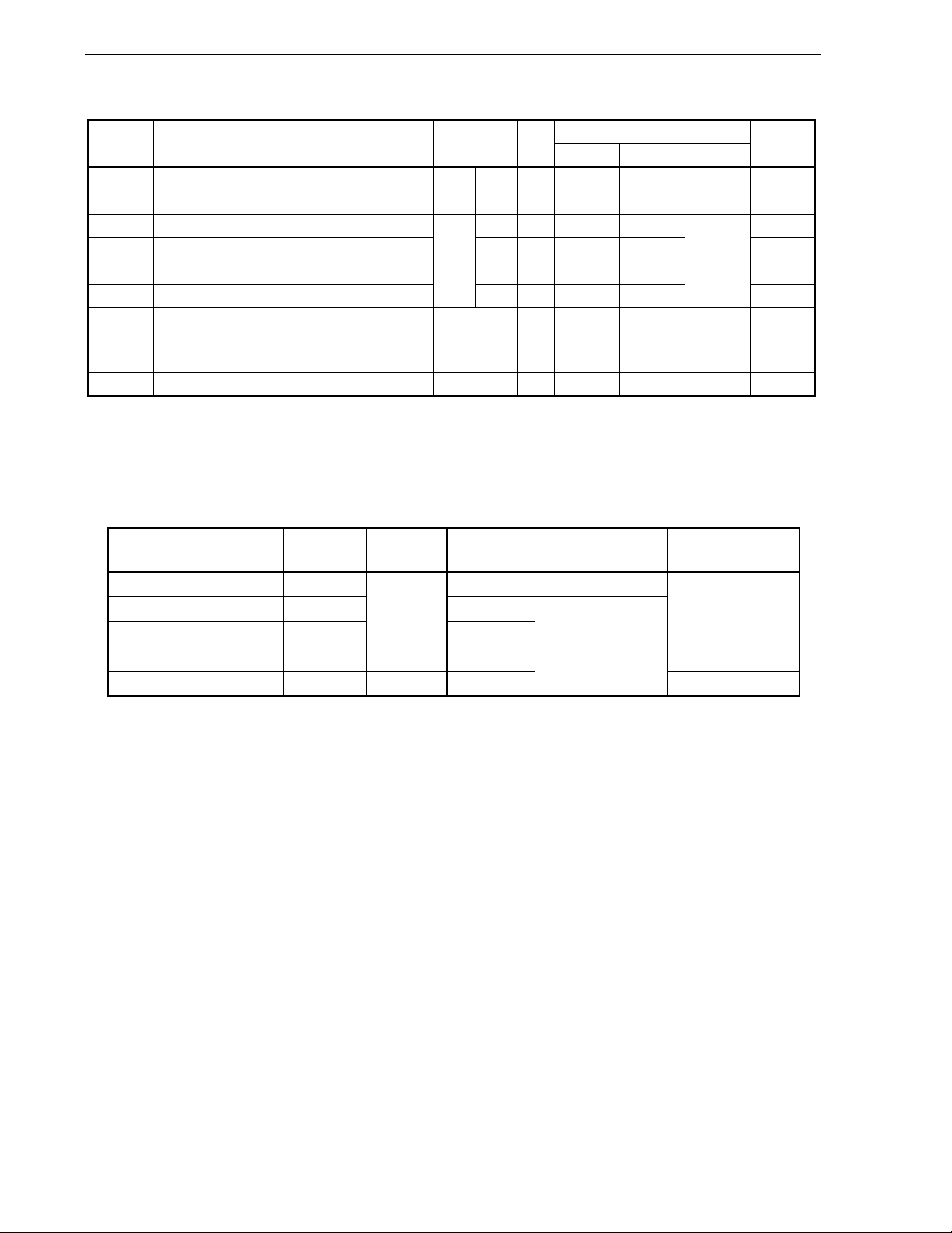
CHAPTER 3 CPU ARCHITECTURE
Table 3-7. Special Function Register List (4/4)
Manipulatable Bit Unit Address Special Function Register (SFR) Name Symbol R/W
1 Bit 8 Bits 16 Bits
FFE6H Interrupt mask flag register 1L MK1 MK1L R/W
FFE7H Interrupt mask flag register 1H MK1H R/W
FFE8H Priority specification flag register 0L PR0 PR0L R/W
FFE9H Priority specification flag register 0H PR0H R/W
FFEAH Priority specification flag register 1L PR1 PR1L R/W
FFEBH Priority specification flag register 1H PR1H R/W
FFF0H Internal memory size switching register
FFF4H Internal expansion RAM size switching
register
Note 1
Note 1
IMS R/W
IXS R/W
FFFBH Processor clock control register PCC R/W
√ √
√ √
√ √
√ √
√ √
√ √
− √ −
− √ −
√ √ −
√
√
√
Notes 1. Regardless of the internal memory capacity, the initial values of the internal memory size switching register
(IMS) and internal expansion RAM size switching register (IXS) of all products in the 78K0/KC2 are fixed
(IMS = CFH, IXS = 0CH). Therefore, set the value corresponding to each product as indicated below.
Flash Memory Version
IMS IXS
(78K0/KC2)
μ
PD78F0511 04H 16 KB 768 bytes
μ
PD78F0512 C6H 24 KB
μ
PD78F0513, 78F0513D
μ
PD78F0514 CCH 0AH 48 KB 1 KB
μ
PD78F0515, 78F0515D
Note 2
C8H
Note 2
CFH 08H 60 KB
0CH
ROM
Capacity
32 KB
Internal High-Speed
RAM Capacity
1 KB
Internal Expansion
RAM Capacity
−
2 KB
<R>
2. The ROM and RAM capacities of the products with the on-chip debug function can be debugged by setting
IMS and IXS, according to the debug target products. Set IMS and IXS according to the debug target
products.
After
Reset
FFH
FFH
FFH
FFH
FFH
FFH
CFH
0CH
01H
74
User’s Manual U17336EJ5V0UD
Page 75
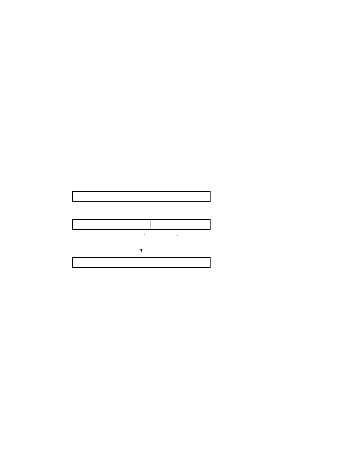
CHAPTER 3 CPU ARCHITECTURE
3.3 Instruction Address Addressing
An instruction address is determined by contents of the program counter (PC), and is normally incremented (+1 for
each byte) automatically according to the number of bytes of an instruction to be fetched each time another instruction
is executed. When a branch instruction is executed, the branch destination information is set to PC and branched by
the following addressing (for details of instructions, refer to the 78K/0 Series Instructions User’s Manual (U12326E)).
3.3.1 Relative addressing
[Function]
The value obtained by adding 8-bit immediate data (displacement value: jdisp8) of an instruction code to the
start address of the following instruction is transferred to the program counter (PC) and branched. The
displacement value is treated as signed two’s complement data (−128 to +127) and bit 7 becomes a sign bit.
In other words, relative addressing consists of relative branching from the start address of the following
instruction to the −128 to +127 range.
This function is carried out when the BR $addr16 instruction or a conditional branch instruction is executed.
[Illustration]
15 0
PC
+
15 0
876
PC indicates the start address
...
of the instruction after the BR instruction.
α
15 0
PC
When S = 0, all bits of are 0.
When S = 1, all bits of are 1.
α
α
S
jdisp8
User’s Manual U17336EJ5V0UD
75
Page 76
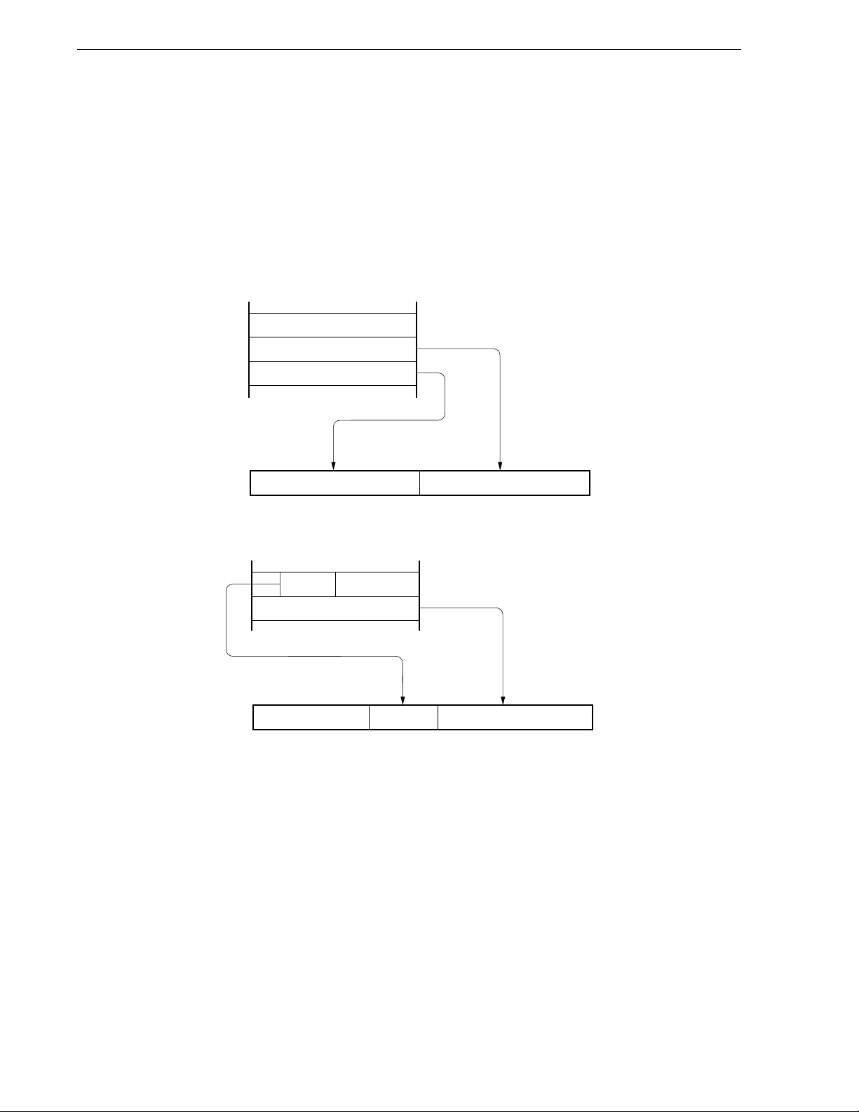
CHAPTER 3 CPU ARCHITECTURE
3.3.2 Immediate addressing
[Function]
Immediate data in the instruction word is transferred to the program counter (PC) and branched.
This function is carried out when the CALL !addr16 or BR !addr16 or CALLF !addr11 instruction is executed.
CALL !addr16 and BR !addr16 instructions can be branched to the entire memory space.
The CALLF !addr11 instruction is branched to the 0800H to 0FFFH area.
[Illustration]
In the case of CALL !addr16 and BR !addr16 instructions
70
CALL or BR
Low Addr.
High Addr.
15 0
PC
In the case of CALLF !addr11 instruction
15 0
PC
00001
87
70
643
10–8
fa
CALLF
fa
7–0
11 10
87
76
User’s Manual U17336EJ5V0UD
Page 77
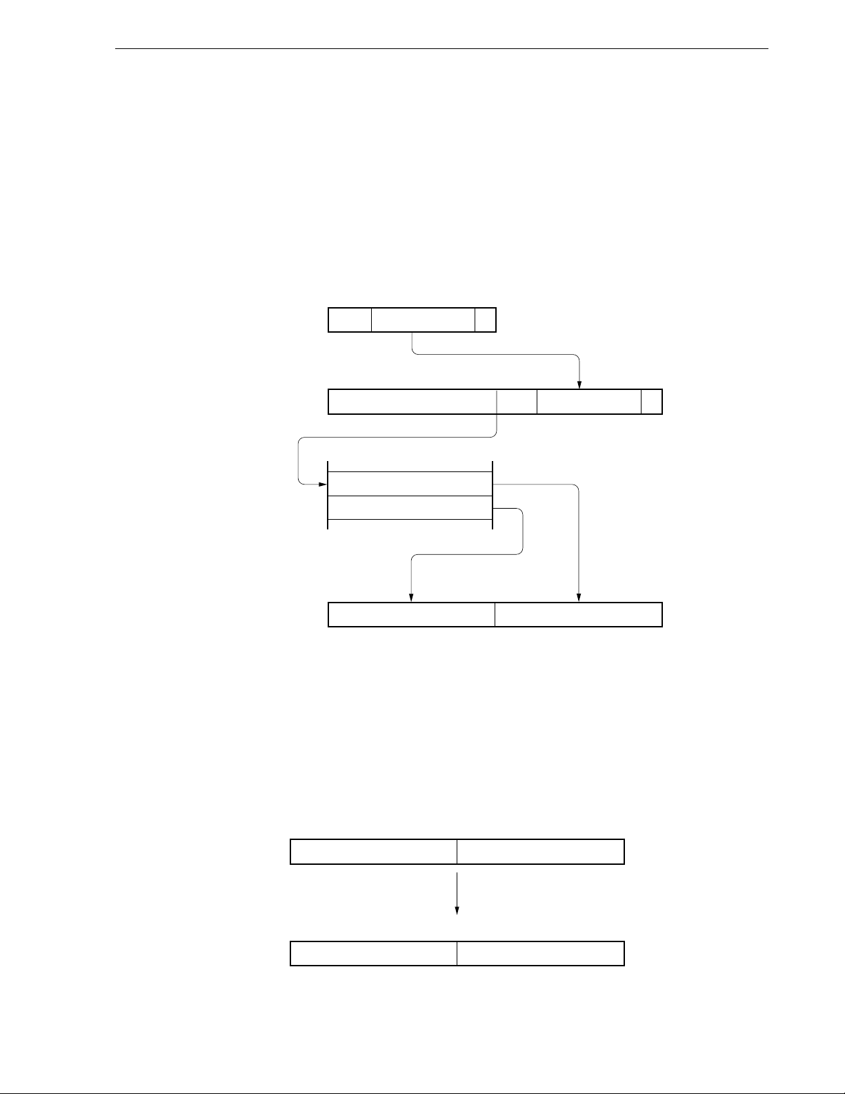
CHAPTER 3 CPU ARCHITECTURE
3.3.3 Table indirect addressing
[Function]
Table contents (branch destination address) of the particular location to be addressed by bits 1 to 5 of the
immediate data of an operation code are transferred to the program counter (PC) and branched.
This function is carried out when the CALLT [addr5] instruction is executed.
This instruction references the address stored in the memory table from 40H to 7FH, and allows branching to
the entire memory space.
[Illustration]
765 10
Operation code
ta
4–0
111
Effective address
Effective address+1
15 1
01
00000000
Memory (Table)
70
Low Addr.
High Addr.
15 0
PC
87
65 0
87
0
3.3.4 Register addressing
[Function]
Register pair (AX) contents to be specified with an instruction word are transferred to the program counter (PC)
and branched.
This function is carried out when the BR AX instruction is executed.
[Illustration]
70
07
rp
15 0
PC
AX
87
User’s Manual U17336EJ5V0UD
77
Page 78
CHAPTER 3 CPU ARCHITECTURE
3.4 Operand Address Addressing
The following methods are available to specify the register and memory (addressing) to undergo manipulation
during instruction execution.
3.4.1 Implied addressing
[Function]
The register that functions as an accumulator (A and AX) among the general-purpose registers is automatically
(implicitly) addressed.
Of the 78K0/KC2 instruction words, the following instructions employ implied addressing.
Instruction Register to Be Specified by Implied Addressing
MULU A register for multiplicand and AX register for product storage
DIVUW AX register for dividend and quotient storage
ADJBA/ADJBS A register for storage of numeric values that become decimal correction targets
ROR4/ROL4 A register for storage of digit data that undergoes digit rotation
[Operand format]
Because implied addressing can be automatically determined with an instruction, no particular operand format is
necessary.
[Description example]
In the case of MULU X
With an 8-bit × 8-bit multiply instruction, the product of A register and X register is stored in AX. In this example,
the A and AX registers are specified by implied addressing.
78
User’s Manual U17336EJ5V0UD
Page 79
CHAPTER 3 CPU ARCHITECTURE
3.4.2 Register addressing
[Function]
The general-purpose register to be specified is accessed as an operand with the register bank select flags
(RBS0 to RBS1) and the register specify codes of an operation code.
Register addressing is carried out when an instruction with the following operand format is executed. When an
8-bit register is specified, one of the eight registers is specified with 3 bits in the operation code.
[Operand format]
Identifier Description
r X, A, C, B, E, D, L, H
rp AX, BC, DE, HL
‘r’ and ‘rp’ can be described by absolute names (R0 to R7 and RP0 to RP3) as well as function names (X, A, C,
B, E, D, L, H, AX, BC, DE, and HL).
[Description example]
MOV A, C; when selecting C register as r
Operation code 0 1 1 0 0 0 1 0
Register specify code
INCW DE; when selecting DE register pair as rp
Operation code 1 0 0 0 0 1 0 0
Register specify code
User’s Manual U17336EJ5V0UD
79
Page 80
CHAPTER 3 CPU ARCHITECTURE
3.4.3 Direct addressing
[Function]
The memory to be manipulated is directly addressed with immediate data in an instruction word becoming an
operand address.
[Operand format]
Identifier Description
addr16 Label or 16-bit immediate data
[Description example]
MOV A, !0FE00H; when setting !addr16 to FE00H
Operation code 10001110 OP code
00000000 00H
11111110 FEH
[Illustration]
07
OP code
addr16 (lower)
addr16 (upper)
Memory
80
User’s Manual U17336EJ5V0UD
Page 81
CHAPTER 3 CPU ARCHITECTURE
3.4.4 Short direct addressing
[Function]
The memory to be manipulated in the fixed space is directly addressed with 8-bit data in an instruction word.
This addressing is applied to the 256-byte space FE20H to FF1FH. Internal high-speed RAM and special
function registers (SFRs) are mapped at FE20H to FEFFH and FF00H to FF1FH, respectively.
The SFR area (FF00H to FF1FH) where short direct addressing is applied is a part of the overall SFR area.
Ports that are frequently accessed in a program and compare and capture registers of the timer/event counter
are mapped in this area, allowing SFRs to be manipulated with a small number of bytes and clocks.
When 8-bit immediate data is at 20H to FFH, bit 8 of an effective address is set to 0. When it is at 00H to 1FH,
bit 8 is set to 1. See the [Illustration] shown below.
[Operand format]
Identifier Description
saddr Immediate data that indicate label or FE20H to FF1FH
saddrp Immediate data that indicate label or FE20H to FF1FH (even address only)
[Description example]
LB1 EQU 0FE30H ; Defines FE30H by LB1.
:
MOV LB1, A ; When LB1 indicates FE30H of the saddr area and the value of register A is transferred to
that address
Operation code 1 1 1 1 0 0 1 0 OP code
0 0 1 1 0 0 0 0 30H (saddr-offset)
[Illustration]
07
OP code
saddr-offset
15
Effective address
1
111111
When 8-bit immediate data is 20H to FFH,
When 8-bit immediate data is 00H to 1FH,
87
α
α
= 0
α
= 1
User’s Manual U17336EJ5V0UD
Short direct memory
0
81
Page 82
CHAPTER 3 CPU ARCHITECTURE
3.4.5 Special function register (SFR) addressing
[Function]
A memory-mapped special function register (SFR) is addressed with 8-bit immediate data in an instruction word.
This addressing is applied to the 240-byte spaces FF00H to FFCFH and FFE0H to FFFFH. However, the SFRs
mapped at FF00H to FF1FH can be accessed with short direct addressing.
[Operand format]
Identifier Description
sfr Special function register name
sfrp 16-bit manipulatable special function register name (even address only)
[Description example]
MOV PM0, A; when selecting PM0 (FF20H) as sfr
Operation code 1 1110110 OP code
0 0100000 20H (sfr-offset)
[Illustration]
07
Effective address
OP code
sfr-offset
15
1
111111
87
1
SFR
0
82
User’s Manual U17336EJ5V0UD
Page 83
CHAPTER 3 CPU ARCHITECTURE
3.4.6 Register indirect addressing
[Function]
Register pair contents specified by a register pair specify code in an instruction word and by a register bank
select flag (RBS0 and RBS1) serve as an operand address for addressing the memory.
[Operand format]
Identifier Description
[DE], [HL]
−
[Description example]
MOV A, [DE]; when selecting [DE] as register pair
Operation code 1 0 0 0 0 1 0 1
[Illustration]
16 08D7
DE
The contents of the memory
addressed are transferred.
A
7 0
E
Memory
The memory address
07
specified with the
register pair DE
User’s Manual U17336EJ5V0UD
83
Page 84
CHAPTER 3 CPU ARCHITECTURE
3.4.7 Based addressing
[Function]
8-bit immediate data is added as offset data to the contents of the base register, that is, the HL register pair in
the register bank specified by the register bank select flag (RBS0 and RBS1), and the sum is used to address
the memory. Addition is performed by expanding the offset data as a positive number to 16 bits. A carry from
the 16th bit is ignored.
[Operand format]
Identifier Description
−
[HL + byte]
[Description example]
MOV A, [HL + 10H]; when setting byte to 10H
Operation code 10101110
00010000
[Illustration]
16 08H7
HL
The contents of the memory
addressed are transferred.
7 0
A
L
Memory
07
+10H
84
User’s Manual U17336EJ5V0UD
Page 85
CHAPTER 3 CPU ARCHITECTURE
3.4.8 Based indexed addressing
[Function]
The B or C register contents specified in an instruction word are added to the contents of the base register, that
is, the HL register pair in the register bank specified by the register bank select flag (RBS0 and RBS1), and the
sum is used to address the memory. Addition is performed by expanding the B or C register contents as a
positive number to 16 bits. A carry from the 16th bit is ignored.
[Operand format]
Identifier Description
[HL + B], [HL + C]
−
[Description example]
MOV A, [HL +B]; when selecting B register
Operation code 1 0 1 0 1 0 1 1
[Illustration]
16 0
78
HL
The contents of the memory
addressed are transferred.
7 0
A
H
+
L
B
Memory
07
07
User’s Manual U17336EJ5V0UD
85
Page 86

CHAPTER 3 CPU ARCHITECTURE
Page 87
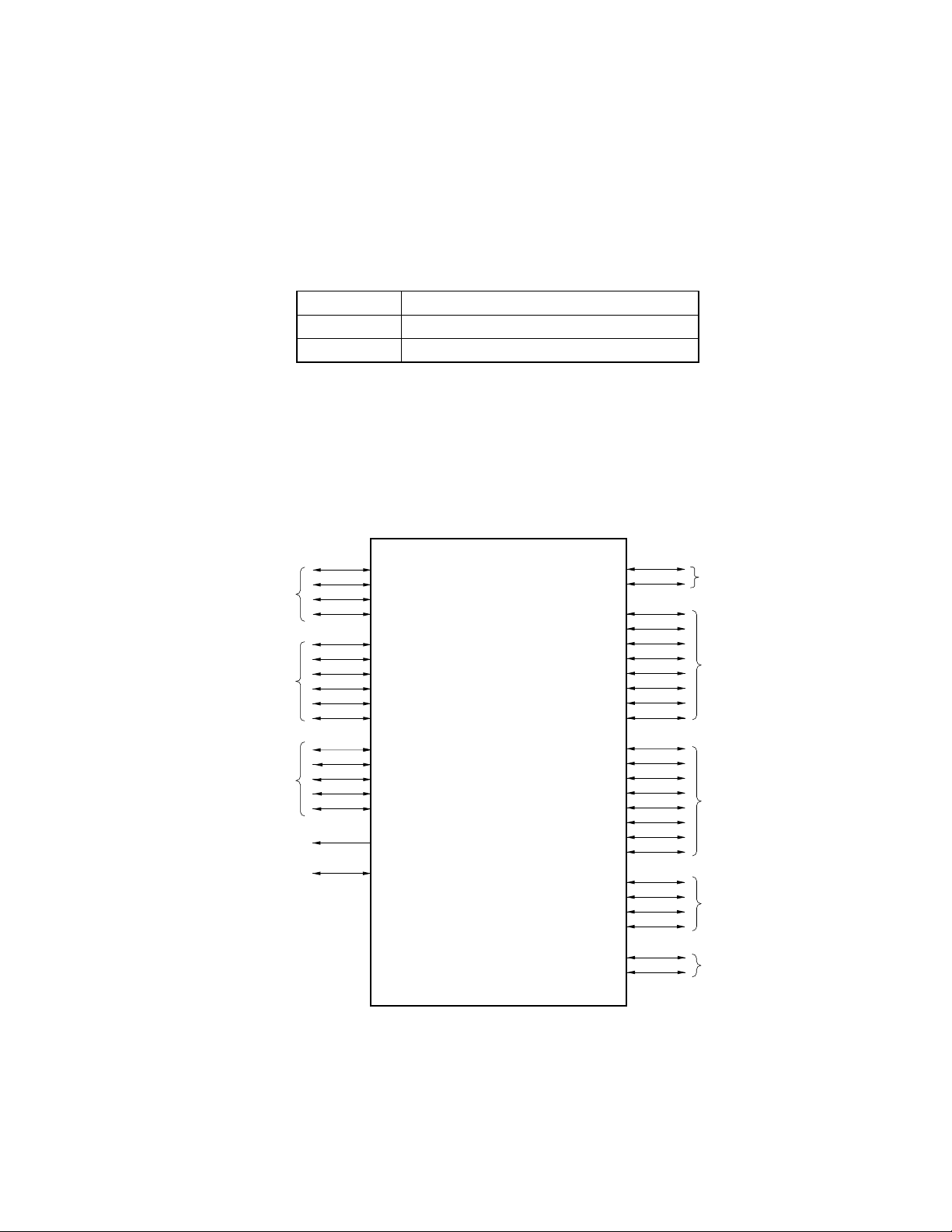
CHAPTER 4 PORT FUNCTIONS
4.1 Port Functions
There are two types of pin I/O buffer power supplies: AV
supplies and the pins is shown below.
Table 4-1. Pin I/O Buffer Power Supplies
Power Supply Corresponding Pins
AVREF P20 to P27
VDD Pins other than P20 to P27
78K0/KC2 products are provided with the ports shown in Figure 4-1, which enable variety of control operations.
The functions of each port are shown in Table 4-2.
In addition to the function as digital I/O ports, these ports have several alternate functions. For details of the
alternate functions, see CHAPTER 2 PIN FUNCTIONS.
Figure 4-1. Port Types
REF and VDD. The relationship between these power
<R>
P60
Port 6
P63
P00
P01
P10
Port 0
P70
Port 7
P71
P72
P73
P74
P75
P120
Note 1
Note 1
Note 2
Note 2
P17
P20
Port 1
Port 12
Port 2
Port 13
Port 14
P124
P130
P140
Note 2
Note 2
P26
P27
Note 1
Note 1
P30
Port 3
P33
Note 1
P40
P41
Note 1
Port 4
Notes 1. 44-pin and 48-pin products only
2. 48-pin products only
User’s Manual U17336EJ5V0UD
87
Page 88
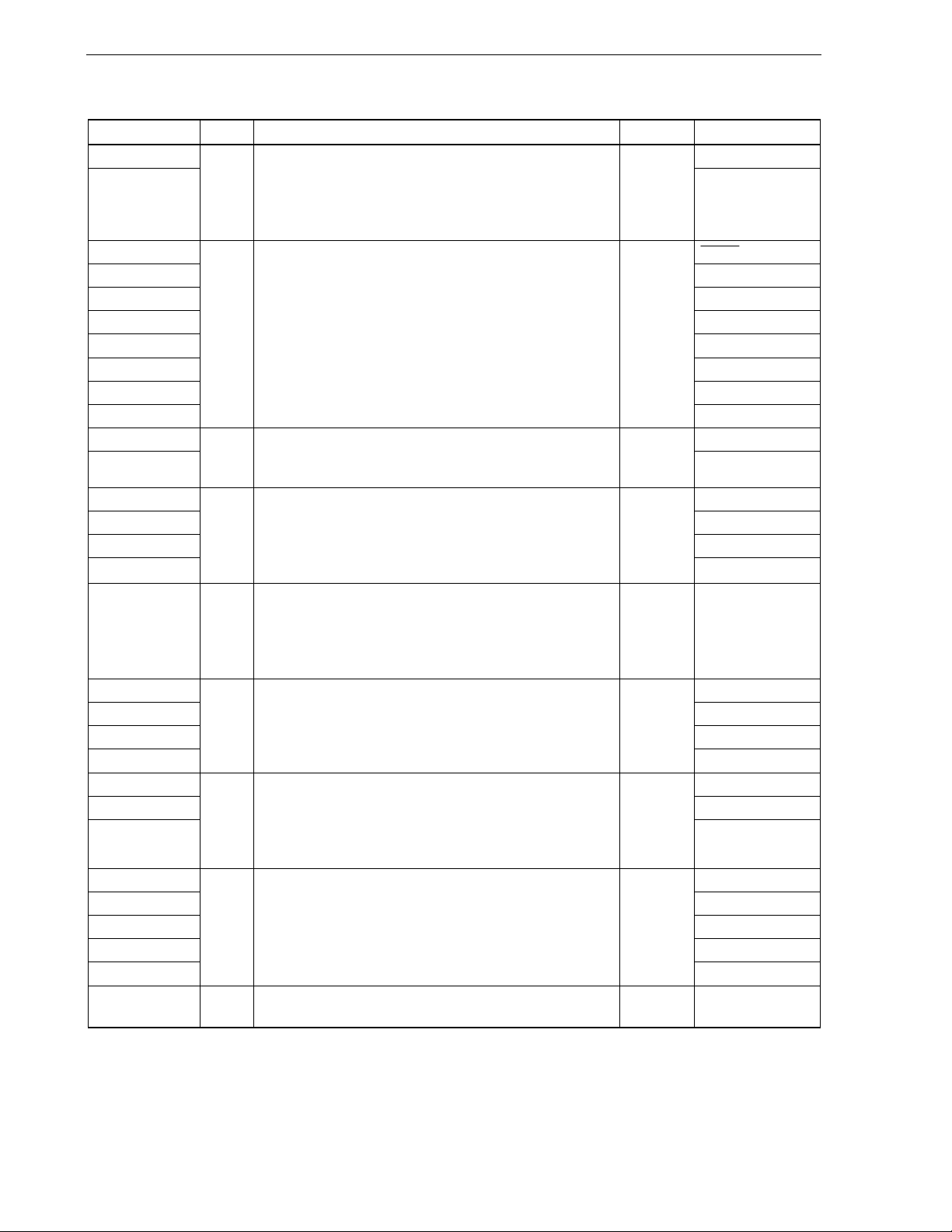
CHAPTER 4 PORT FUNCTIONS
Table 4-2. Port Functions (1/2)
Function Name I/O Function After Reset Alternate Function
P00 TI000
P01
I/O Port 0.
2-bit I/O port.
Input port
TI010/TO00
Input/output can be specified in 1-bit units.
Use of an on-chip pull-up resistor can be specified by a software
setting.
P10 SCK10/TxD0
P11 SI10/RxD0
P12 SO10
P13 TxD6
I/O Port 1.
8-bit I/O port.
Input/output can be specified in 1-bit units.
Use of an on-chip pull-up resistor can be specified by a software
setting.
Input port
P14 RxD6
P15 TOH0
P16 TOH1/INTP5
P17
P20 to P25 ANI0 to ANI5
Note 1
P26
and P27
I/O Port 2.
Note 1
8-bit I/O port.
Analog
input
TI50/TO50
ANI6
Input/output can be specified in 1-bit units.
P30 INTP1
P31 INTP2/OCD1A
P32 INTP3/OCD1B
P33
Note 1
P40
and P41
I/O Port 3.
4-bit I/O port.
Input/output can be specified in 1-bit units.
Use of an on-chip pull-up resistor can be specified by a software
setting.
Note 1
I/O Port 4.
Input port
TI51/TO51/INTP4
Input port
2-bit I/O port.
Input/output can be specified in 1-bit units.
Use of an on-chip pull-up resistor can be specified by a software
setting.
P60 SCL0
P61 SDA0
P62 EXSCL0
I/O Port 6.
4-bit I/O port.
Output of P60 to P63 is N-ch open-drain output (6 V tolerance).
Input/output can be specified in 1-bit units.
Input port
P63
P70 and P71 KR0 and KR1
Note 1
P72
and P73
Note 3
P74
and P75
I/O Port 7.
Note 1
KR2
Note 3
6-bit I/O port.
Input/output can be specified in 1-bit units.
Use of an on-chip pull-up resistor can be specified by a software
Input port
Note 1
setting.
P120 INTP0/EXLVI
P121 X1/OCD0A
P122 X2/EXCLK/OCD0B
P123 XT1
I/O Port 12.
5-bit I/O port.
Input/output can be specified in 1-bit units.
Only for P120, use of an on-chip pull-up resistor can be
specified by a software setting.
P124
Note 3
P130
Output Port 13.
Input port
XT2/EXCLKS
Output port
1-bit output-only port.
Notes 1. 44-pin and 48-pin products only
<R>
For the 38-pin products, be sure to set bits 6 and 7 of PM2 to “1”, and bits 0 and 1 of PM4, bits 2 and 3 of
PM7, bits 6 and 7 of P2, bits 0 and 1 of P4, and bits 2 and 3 of P7 to “0”.
2.
μ
PD78F0513D and 78F0515D only
3. 48-pin products only
Note 1
and ANI7
and KR3
Note 1
Note 2
Note 2
−
−
Note 1
−
Note 2
Note 2
−
88
User’s Manual U17336EJ5V0UD
Page 89
Function Name I/O Function After Reset Alternate Function
Note
P140
I/O
Note 48-pin products only
4.2 Port Configuration
Ports include the following hardware.
Item Configuration
Control registers
<R>
Port
<R>
Pull-up resistor
Note 48-pin products only
CHAPTER 4 PORT FUNCTIONS
Table 4-2. Port Functions (2/2)
Port 14.
1-bit I/O port.
Input/output can be specified in 1-bit units.
Use of an on-chip pull-up resistor can be specified by a
software setting.
Table 4-3. Port Configuration
Port mode register (PM0 to PM4, PM6, PM7, PM12, PM14
Port register (P0 to P4, P6, P7, P12, P13
Pull-up resistor option register (PU0, PU1, PU3, PU4, PU7, PU12, PU14
A/D port configuration register (ADPC)
• 38-pin products
Total: 31 (CMOS I/O: 27, CMOS output: 0, N-ch open drain I/O: 4)
• 44-pin products
Total: 37 (CMOS I/O: 33, CMOS output: 0, N-ch open drain I/O: 4)
• 48-pin products
Total: 41 (CMOS I/O: 36, CMOS output: 1, N-ch open drain I/O: 4)
• 38-pin products Total: 17
• 44-pin products Total: 21
• 48-pin products Total: 24
Note
, P14
Note
)
Input port PCL/INTP6
Note
)
Note
)
Note
User’s Manual U17336EJ5V0UD
89
Page 90
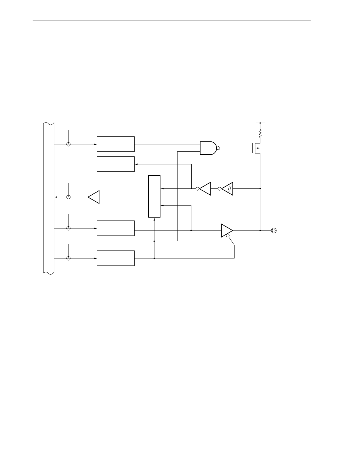
CHAPTER 4 PORT FUNCTIONS
4.2.1 Port 0
Port 0 is a 2-bit I/O port with an output latch. Port 0 can be set to the input mode or output mode in 1-bit units
using port mode register 0 (PM0). When the P00 and P01 pins are used as an input port, use of an on-chip pull-up
resistor can be specified in 1-bit units by pull-up resistor option register 0 (PU0).
This port can also be used for timer I/O.
Reset signal generation sets port 0 to input mode.
Figures 4-2 and 4-3 show block diagrams of port 0.
Figure 4-2. Block Diagram of P00
V
DD
WR
PU
PU0
PU00
Alternate function
RD
Internal bus
WR
WR
PORT
PM
P0
Output latch
(P00)
PM0
PM00
P0: Port register 0
PU0: Pull-up resistor option register 0
PM0: Port mode register 0
RD: Read signal
WR××: Write signal
P-ch
Selector
P00/TI000
90
User’s Manual U17336EJ5V0UD
Page 91
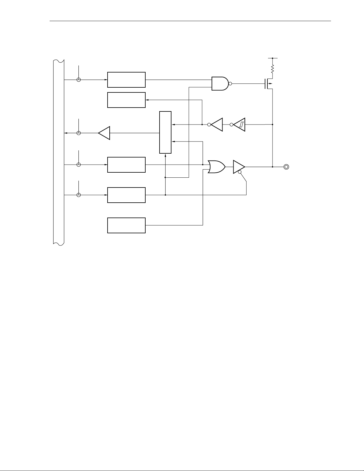
CHAPTER 4 PORT FUNCTIONS
Figure 4-3. Block Diagram of P01
V
DD
PU
WR
PU0
Internal bus
PU01
Alternate function
RD
WR
PORT
P0
Output latch
(P01)
WR
PM
PM0
PM01
Alternate function
P0: Port register 0
PU0: Pull-up resistor option register 0
PM0: Port mode register 0
RD: Read signal
WR××: Write signal
P-ch
Selector
P01/TI010/TO00
User’s Manual U17336EJ5V0UD
91
Page 92
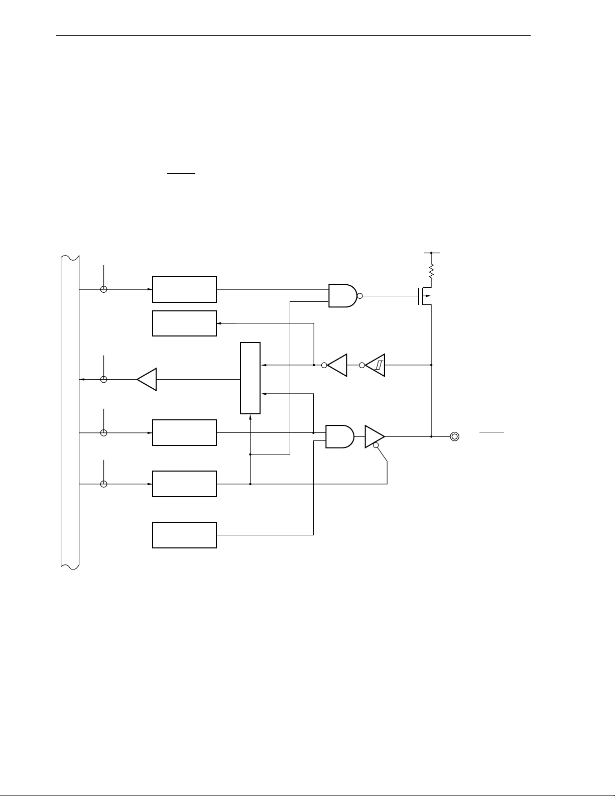
CHAPTER 4 PORT FUNCTIONS
4.2.2 Port 1
Port 1 is an 8-bit I/O port with an output latch. Port 1 can be set to the input mode or output mode in 1-bit units
using port mode register 1 (PM1). When the P10 to P17 pins are used as an input port, use of an on-chip pull-up
resistor can be specified in 1-bit units by pull-up resistor option register 1 (PU1).
This port can also be used for external interrupt request input, serial interface data I/O, clock I/O, and timer I/O.
Reset signal generation sets port 1 to input mode.
Figures 4-4 to 4-8 show block diagrams of port 1.
Caution To use P10/SCK10/TxD0 and P12/SO10 as general-purpose ports, set serial operation mode
register 10 (CSIM10) and serial clock selection register 10 (CSIC10) to the default status (00H).
Figure 4-4. Block Diagram of P10
V
DD
WR
PU
PU1
Internal bus
PU10
Alternate
function
RD
WR
WR
PORT
PM
P1
Output latch
(P10)
PM1
PM10
Alternate
function
P1: Port register 1
PU1: Pull-up resistor option register 1
PM1: Port mode register 1
RD: Read signal
WR××: Write signal
P-ch
Selector
P10/SCK10/TxD0
92
User’s Manual U17336EJ5V0UD
Page 93
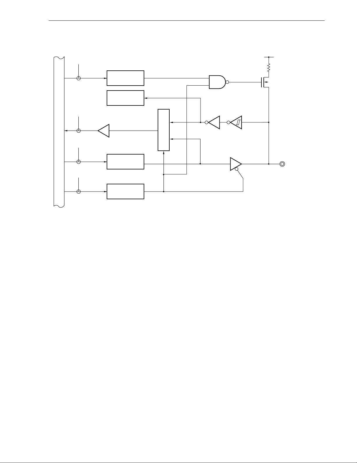
CHAPTER 4 PORT FUNCTIONS
Figure 4-5. Block Diagram of P11 and P14
V
DD
WR
PU
PU1
PU11, PU14
Alternate
function
RD
Internal bus
WR
PORT
P1
Output latch
(P11, P14)
WR
PM
PM1
PM11, PM14
P1: Port register 1
PU1: Pull-up resistor option register 1
PM1: Port mode register 1
RD: Read signal
WR××: Write signal
P-ch
Selector
P11/SI10/RxD0,
P14/RxD6
User’s Manual U17336EJ5V0UD
93
Page 94
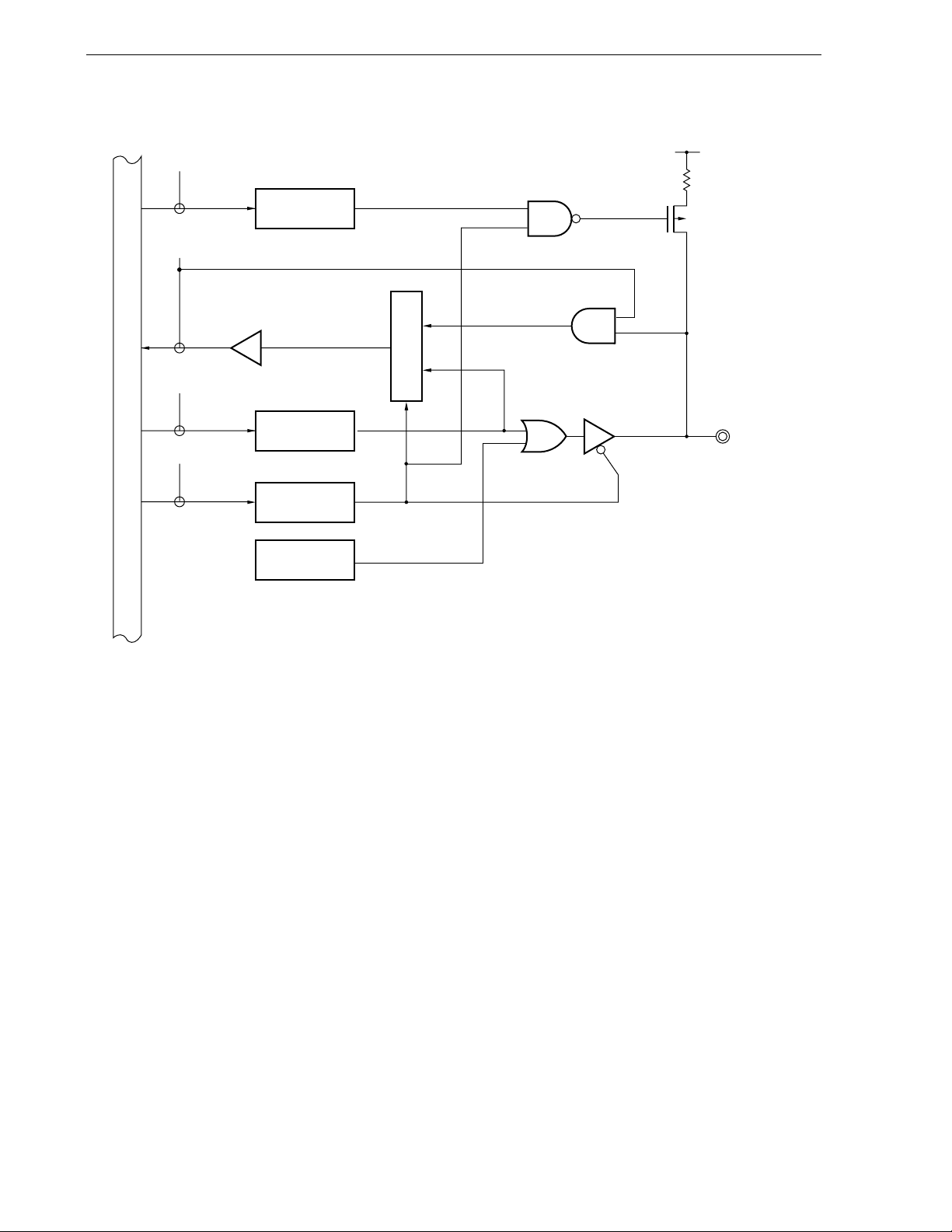
CHAPTER 4 PORT FUNCTIONS
Figure 4-6. Block Diagram of P12 and P15
V
DD
WR
PU
PU1
PU12, PU15
RD
PORT
WR
P1
Output latch
Internal bus
WR
PM
(P12, P15)
PM1
PM12, PM15
Alternate
function
P1: Port register 1
PU1: Pull-up resistor option register 1
PM1: Port mode register 1
RD: Read signal
WR××: Write signal
P-ch
Selector
P12/SO10
P15/TOH0
94
User’s Manual U17336EJ5V0UD
Page 95
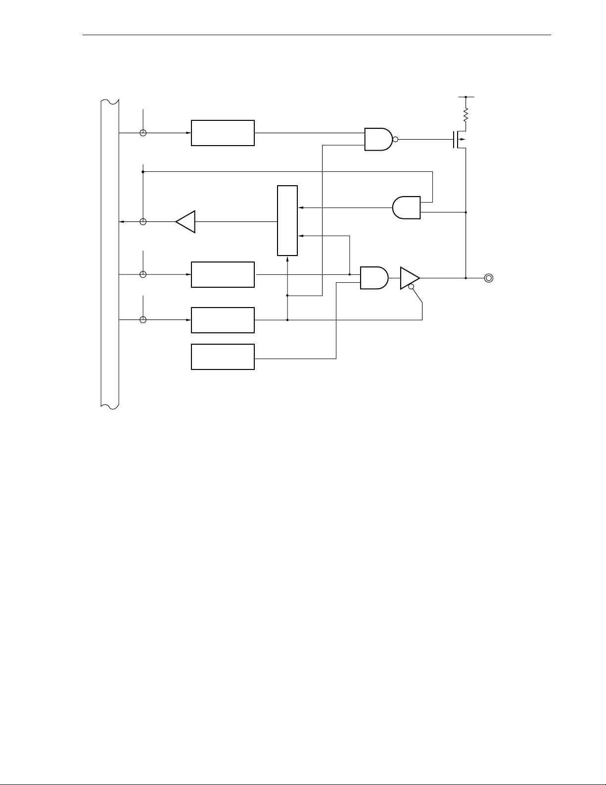
CHAPTER 4 PORT FUNCTIONS
Figure 4-7. Block Diagram of P13
V
DD
PU
WR
PU1
PU13
RD
PORT
WR
P1
Internal bus
WR
PM
Output latch
(P13)
PM1
PM13
Alternate
function
P1: Port register 1
PU1: Pull-up resistor option register 1
PM1: Port mode register 1
RD: Read signal
WR××: Write signal
P-ch
Selector
P13/TxD6
User’s Manual U17336EJ5V0UD
95
Page 96
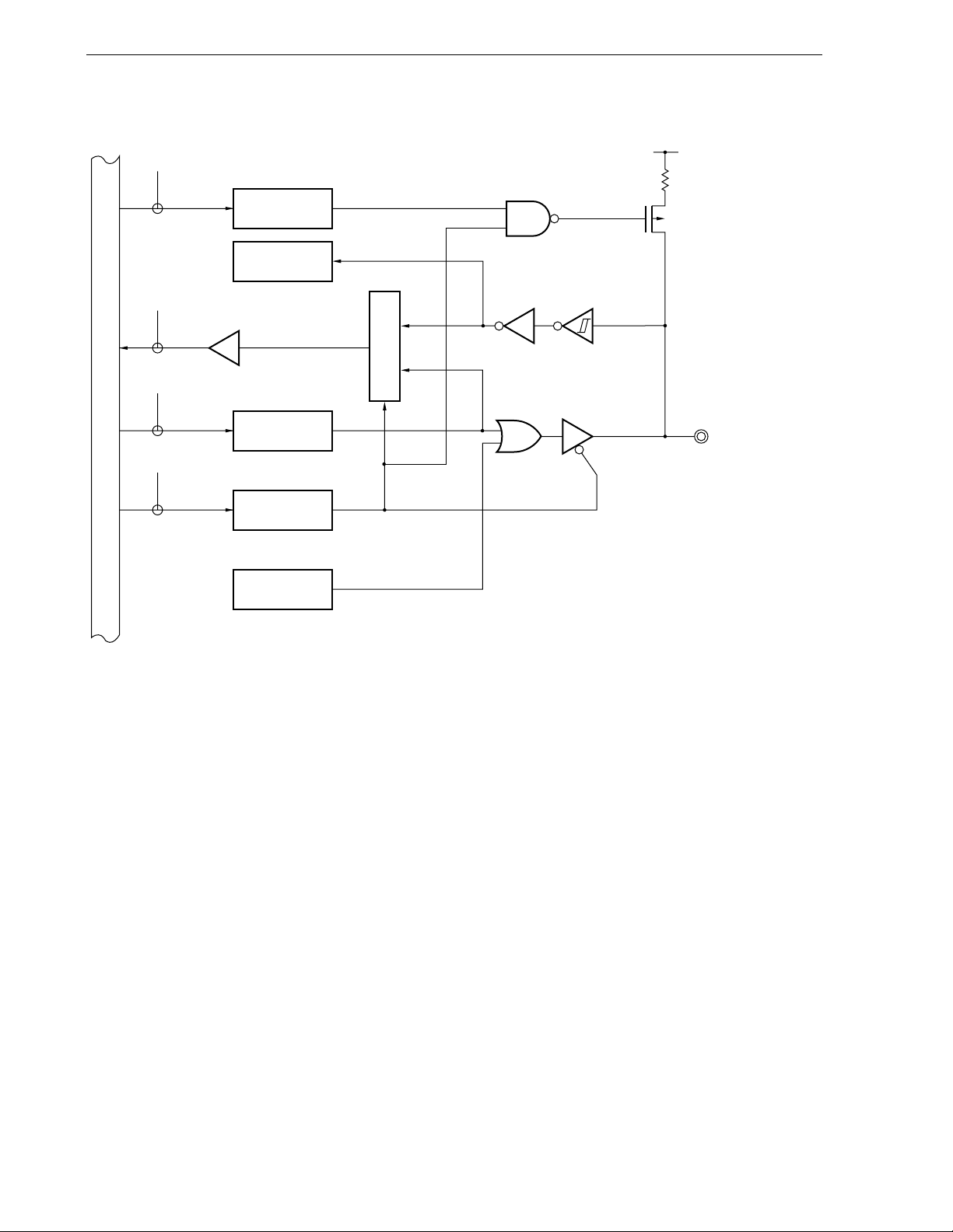
CHAPTER 4 PORT FUNCTIONS
Figure 4-8. Block Diagram of P16 and P17
VDD
WR
PU
PU1
Internal bus
PU16, PU17
Alternate
function
RD
WR
PORT
WRPM
P1
Output latch
(P16, P17)
PM1
PM16, PM17
Alternate
function
P1: Port register 1
PU1: Pull-up resistor option register 1
PM1: Port mode register 1
RD: Read signal
WR××: Write signal
P-ch
Selector
P16/TOH1/INTP5,
P17/TI50/TO50
96
User’s Manual U17336EJ5V0UD
Page 97
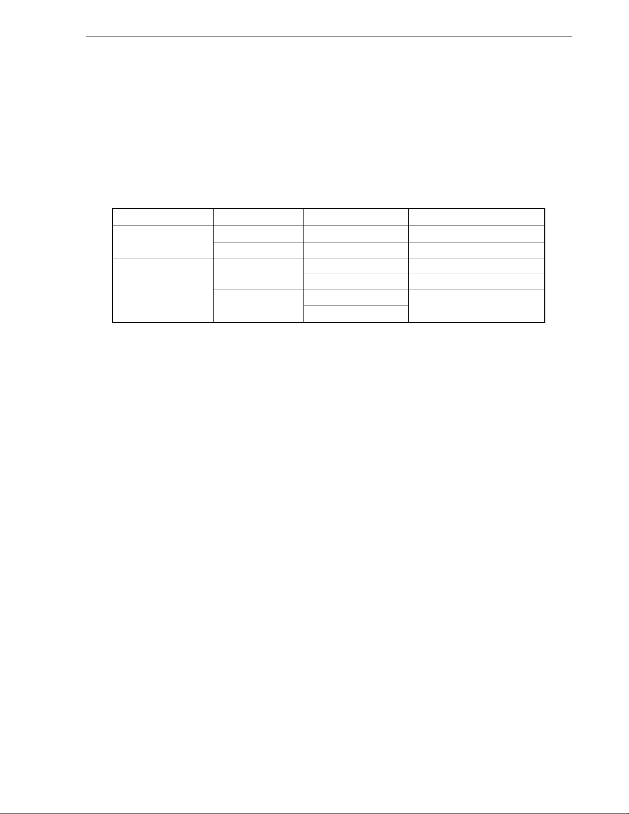
CHAPTER 4 PORT FUNCTIONS
4.2.3 Port 2
Port 2 is an 8-bit I/O port with an output latch. Port 2 can be set to the input mode or output mode in 1-bit units
using port mode register 2 (PM2).
This port can also be used for A/D converter analog input.
To use P20/ANI0 to P27/ANI7
Note
as digital input pins, set them in the digital I/O mode by using the A/D port
configuration register (ADPC) and in the input mode by using PM2. Use these pins starting from the lower bit.
To use P20/ANI0 to P27/ANI7
Note
as digital output pins, set them in the digital I/O mode by using ADPC and in the
output mode by using PM2.
Note
Pins
Digital input Digital I/O selection
Digital output
Setting prohibited
Note
Pins
ADPC PM2 ADS P20/ANI0 to P27/ANI7
Analog input selection
Table 4-4. Setting Functions of P20/ANI0 to P27/ANI7
Input mode
Output mode
Output mode
Selects ANI. Analog input (to be converted) Input mode
Does not select ANI. Analog input (not to be converted)
Selects ANI.
Does not select ANI.
−
−
<R>
<R>
All P20/ANI0 to P27/ANI7
Note
are set in the analog input mode when the reset signal is generated.
Figure 4-9 shows a block diagram of port 2.
Note 38-pin products: P20/ANI0 to P25/ANI5
44-pin and 48-pin products: P20/ANI0 to P27/ANI7
Cautions 1. Make the AV
REF pin the same potential as the VDD pin when port 2 is used as a digital port.
2. For the 38-pin products, be sure to set bits 6 and 7 of PM2 to “1”, and bits 6 and 7 of P2 to “0”.
User’s Manual U17336EJ5V0UD
97
Page 98
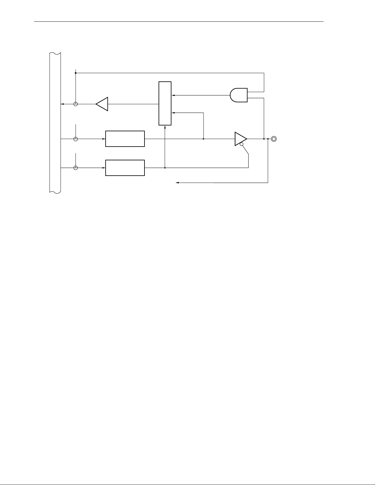
<R>
CHAPTER 4 PORT FUNCTIONS
Figure 4-9. Block Diagram of P20 to P27
RD
PORT
WR
Internal bus
WR
PM
P2
Output latch
(P20 to P27)
PM2
PM20 to PM27
A/D converter
Note 38-pin products: P20/ANI0 to P25/ANI5
44-pin and 48-pin products: P20/ANI0 to P27/ANI7
P2: Port register 2
PM2: Port mode register 2
RD: Read signal
WR××: Write signal
Selector
P20/ANI0 to
P27/ANI7
Note
98
User’s Manual U17336EJ5V0UD
Page 99

<R>
<R>
CHAPTER 4 PORT FUNCTIONS
4.2.4 Port 3
Port 3 is a 4-bit I/O port with an output latch. Port 3 can be set to the input mode or output mode in 1-bit units
using port mode register 3 (PM3). When the P30 to P33 pins are used as an input port, use of an on-chip pull-up
resistor can be specified in 1-bit units by pull-up resistor option register 3 (PU3).
This port can also be used for external interrupt request input and timer I/O.
Reset signal generation sets port 3 to input mode.
Figures 4-10 and 4-11 show block diagrams of port 3.
Cautions 1. In the products with an on-chip debug function (
the P31/INTP2/OCD1A
Note
pin down before a reset release, to prevent malfunction.
μ
PD78F0513D and 78F0515D), be sure to pull
2. For products without an on-chip debug function, with the flash memory of 48 KB or more
(
μ
PD78F0514 and 78F0515), and having a product rank of “I”, “K”, or “E”, and for the
products with an on-chip debug function (
P31/INTP2/OCD1A
Note
as follows when writing the flash memory with a flash memory
μ
PD78F0513D and 78F0515D), connect
programmer.
• P31/INTP2/OCD1A
Note
: Connect to VSS via a resistor (10 kΩ: recommended).
The above connection is not necessary when writing the flash memory by means of self
programming.
Note OCD1A is provided to the
μ
PD78F0513D and 78F0515D only.
Remarks 1. For the product ranks, consult an NEC Electronics sales representative.
2. Only for the
μ
PD78F0513D and 78F0515D, P31 and P32 can be used as on-chip debug mode
setting pins (OCD1A, OCD1B) when the on-chip debug function is used. For how to connect an in-
circuit emulator supporting on-chip debugging (QB-78K0MINI or QB-MINI2), see CHAPTER 26
ON-CHIP DEBUG FUNCTION (
μ
PD78F0513D AND 78F0515D ONLY).
User’s Manual U17336EJ5V0UD
99
Page 100
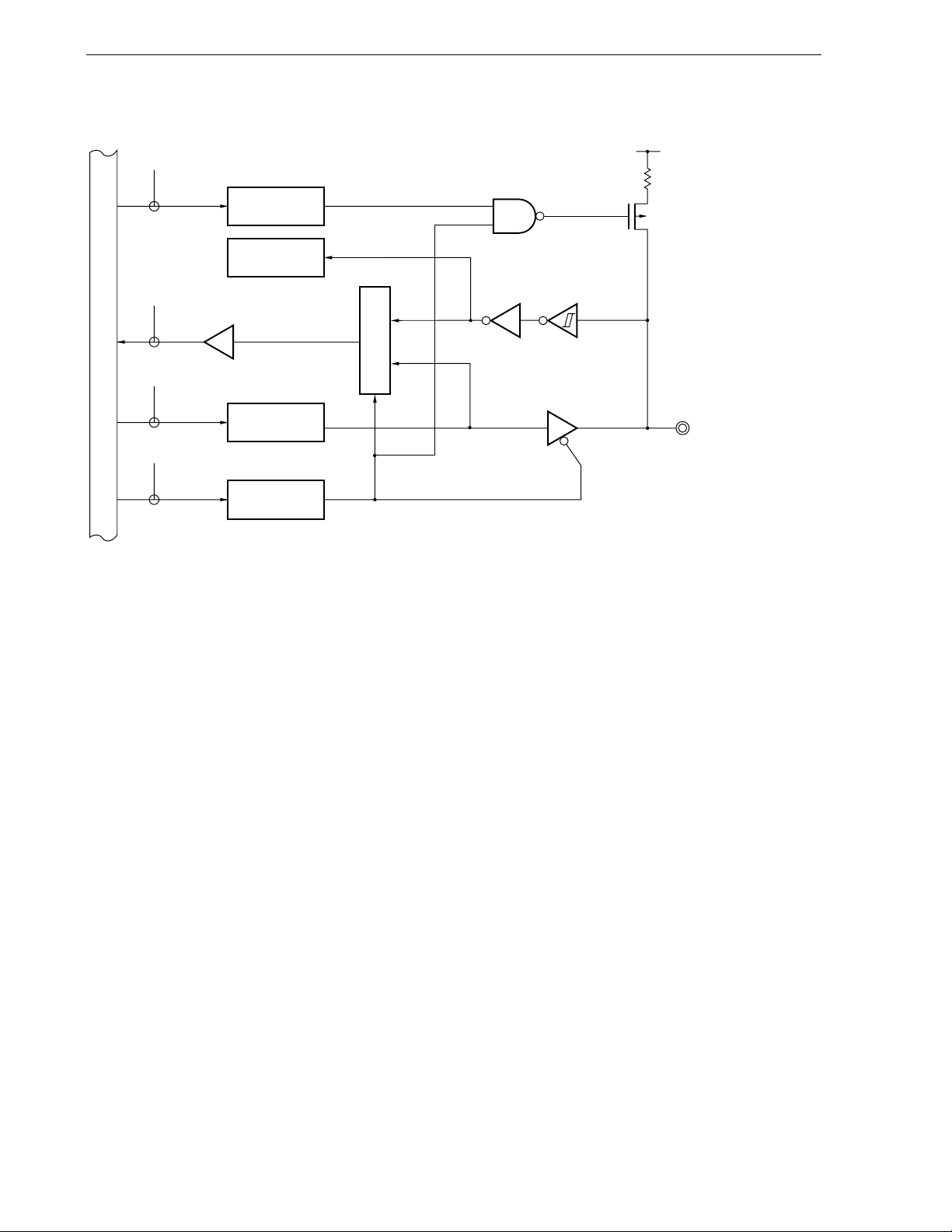
CHAPTER 4 PORT FUNCTIONS
Figure 4-10. Block Diagram of P30 to P32
V
DD
WR
PU
PU3
Internal bus
Note
PU30 to PU32
Alternate
function
RD
WR
PORT
WR
PM
μ
PD78F0513D and 78F0515D only
P3
Output latch
(P30 to P32)
PM3
PM30 to PM32
P3: Port register 3
PU3: Pull-up resistor option register 3
PM3: Port mode register 3
RD: Read signal
WR××: Write signal
Selector
P-ch
P30/INTP1,
P31/INTP2/OCD1A
P32/INTP3/OCD1B
Note
Note
,
100
User’s Manual U17336EJ5V0UD
 Loading...