

Page 1
WITH 3-STATE OUTPUTS NON INVERTING
■ HIGH SPEED:
t
= 5.0 ns (TYP.) at VCC=5V
PD
■ LOW POWER DISSIPATION:
I
=4µA (MAX.) at TA=25°C
CC
■ HIGH NOISE IMMUNITY:
V
NIH=VNIL
■ POWER DOWN PROTECTION ON INPUTS
■ SYMMETRICAL OUTPUT IMPEDANCE:
|I
|=IOL=8mA(MIN)
OH
■ BALANCED PROPAGATION DELAYS:
t
≅ t
PLH
■ OPERATING VOLTAGE RANGE:
V
(OPR) = 2V to 5.5V
CC
■ PIN AND FUNCTION COMPATIBLE WITH
74 SERIES 16373
■ IMPROVED LATCH-UP IMMUNITY
■ LOW NOISE: V
= 28% VCC(MIN.)
PHL
OLP
= 0.9V (MAX.)
74VHC16373
16-BIT D-TYPE L ATCH
TSSOP
ORDER CODES
PACKAGE TUBE T & R
TSSOP 74VHC16373TTR
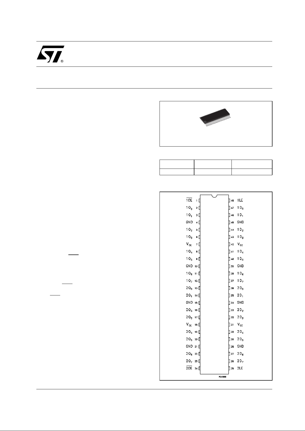
PIN CO NNECTION
DESCRIPTION
The 74VHC16373 is an advanced high-speed
CMOS 16 BIT D-TYPE LATCH with 3 STATE
OUTPUTS NON INVERTING fabricated with
sub-micron s ilicon gate and double-layer metal
wiring C
2
MOS technology.
These 16 bit D-TYPE latches are byte controlled
by two latch enable inputs (nLE) and two out put
enable inputs(nOE
).
While the nLE input is held at a high level, the nQ
outputs will follow the data (D) inputs.
When the nLE is taken LOW, the nQ outputs w ill
be latched at the logic level of D data inputs.
When the (nOE
) input is low, the nQ outputs wil l
be in a normal lo gic s tate (high or low logic level);
when nOE
is at high level ,the outputs will be in a
high impedance state.
Power down protection is provided on all inputs
and 0 to 7V can be ac c epted on inputs with no
regard to the supply vo ltage. This device can be
usedto interface 5V to 3V.
All inputs and outputs are equipped with protection circuits against static discharge, giving them
2KV ESD immunity and transient excess vo ltage.
1/11February 2003
Page 2
74VHC16373
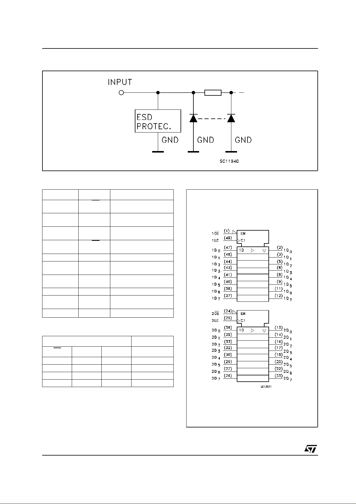
INPUT EQUIVALENT CIRCUIT
PIN DESCRIPTION
PIN No SYMBOL NAME AND FUNCTION
1 1OE
2, 3,5,6,8, 9,
11, 12
13,14,16, 17,
19, 20, 22, 23
24 2OE
25 2LE Latch Enable Input
36,35,33, 32,
30, 29, 27, 26
47,46,44, 43,
41, 40, 38, 37
48 1LE Latch Enable Input
4, 10, 15, 21,
28, 34, 39, 45
7, 18, 31, 42 V
1Q0 to 1Q7 3-State Outputs
2Q0 to 2Q7 3-State Outputs
2D0 to 2D7 Data Inputs
1D0 to 1D7 Data Inputs
GND Ground (0V)
CC
3 State Output Enable
Input (Active LOW)
3 State Output Enable
Input (Active LOW)
Positive Supply Voltage
TRUTH TABLE
INPUTS OUTPUT
OE
HXX Z
L L X NO CHANGE *
LHL L
LHH H
X : Don‘t Care
Z : High Impedance
* : Q outputs arelatched atthe time whenthe LEinput istaken low
logiclevel.
LE D Q
IEC LOGIC SYMBOLS
2/11
Page 3
74VHC16373
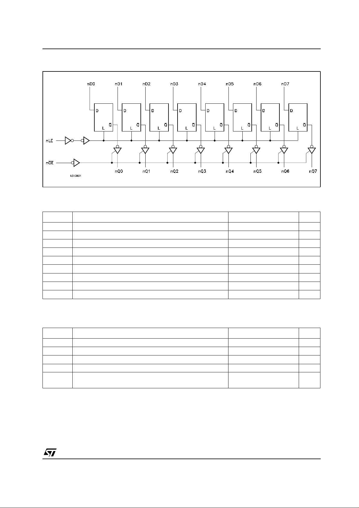
LOGIC DIAGRAM
This logic diagram has not to be used to estimate propagation delays
ABSOLUTE MAXIMUM RATINGS
Symbol Parameter Value Unit
V
CC
V
V
I
IK
I
OK
I
or I
I
CC
T
stg
T
Absolute Maximum Ratings are those values beyond which damage to the device may occur. Functional operation under these conditions is
not implied
Supply Voltage
DC Input Voltage
I
DC Output Voltage -0.5 to VCC+ 0.5
O
DC Input Diode Current
DC Output Diode Current
DC Output Current
O
DC VCCor Ground Current
GND
Storage Temperature
Lead Temperature (10 sec)
L
-0.5 to +7.0 V
-0.5 to +7.0 V
V
-20 mA
± 20 mA
± 25 mA
± 75 mA
-65 to +150 °C
300 °C
RECOMMENDED OPERATING CONDITIONS
Symbol Parameter Value Unit
V
CC
V
V
T
dt/dv
1) VINfrom30% to 70%of V
Supply Voltage
Input Voltage
I
Output Voltage 0 to V
O
Operating Temperature
op
Input Rise and Fall Time (note 1) (V
CC
CC
(V
= 5.0 ± 0.5V)
CC
=3.3±0.3V)
2 to 5.5 V
0 to 5.5 V
CC
-55 to 125 °C
0 to 100
0to20
V
ns/V
3/11
Page 4
74VHC16373
DC SPECIFICATIONS
Symbol Parameter
V
V
V
I
High Level Input
IH
Voltage
V
Low Level Input
IL
Voltage
High Level Output
OH
Voltage
Low Level Output
OL
Voltage
High Impedance
I
OZ
Output Leakage
Current
Input Leakage
I
I
Current
Quiescent Supply
CC
Current
Test Condition Value
V
(V)
CC
T
A
Min. Typ. Max. Min. Max. Min. Max.
-40 to 85°C -55 to 125°C
= 25°C
2.0 1.5 1.5 1.5
3.0to
5.5
0.7V
CC
0.7V
CC
0.7V
CC
2.0 0.5 0.5 0.5
3.0to
5.5
2.0
3.0
4.5
3.0
4.5
2.0
3.0
4.5
3.0
4.5
5.5
0to
5.5
5.5
IO=-50 µA
=-50 µA
I
O
=-50 µA
I
O
=-4 mA
I
O
=-8 mA
I
O
IO=50 µA
=50 µA
I
O
=50 µA
I
O
=4 mA
I
O
=8 mA
I
O
I=VIH
or V
IL
V
VO=VCCor GND
VI= 5.5V or GND
V
I=VCC
or GND
1.9 2.0 1.9 1.9
2.9 3.0 2.9 2.9
4.4 4.5 4.4 4.4
2.58 2.48 2.4
3.94 3.8 3.7
0.3V
CC
0.3V
CC
0.3V
0.0 0.1 0.1 0.1
0.0 0.1 0.1 0.1
0.0 0.1 0.1 0.1
0.36 0.44 0.55
0.36 0.44 0.55
±0.25 ± 2.5 ± 5 µA
± 0.1 ± 1 ± 1 µA
44040µA
CC
Unit
V
V
V
V
4/11
Page 5

AC ELECTRICAL C HARACTERISTICS (Input tr=tf=3ns)
Test Condition Value
Symbol Parameter
V
(V)
t
t
Propagation Delay
PLH
Time
PHL
LE to Qn
3.3
3.3
5.0
5.0
t
t
Propagation Delay
PLH
Time
PHL
Dn to Qn
3.3
3.3
5.0
5.0
t
t
PZH
PZL
Output Enable
Time
3.3
3.3
5.0
5.0
t
t
PHZ
t
OSLH
t
OSHL
(*) Voltagerange is3.3V ± 0.3V
(**) Voltage range is 5.0V ± 0.5V
Note 1 : Parameter guaranteed by design. t
Output Disable
PLZ
Time
t
Pulse Width (LE)
w
HIGH
t
Setup Time Dn to
s
LE HIGH or LOW
t
Hold Time Dn to LE
h
HIGH or LOW
Output to Output
Skew time (note 1)
3.3
5.0
3.3
5.0
3.3
5.0
3.3
5.0
3.3
5.0
C
CC
L
(pF)
(*)
15 5.5 13 1 15 1 15
(*)
50 7 14.5 1 16.5 1 16.5
(**)
15 3.6 8.5 1 9.5 1 9.5
(**)
50 5 9.5 1 10.5 1 10.5
(*)
15 5.5 13 1 15 1 15
(*)
50 7.5 14 1 16 1 16
(**)
15 4 8.2 1 9.5 1 9.5
(**)
50 5 9.2 1 10.5 1 10.5
(*)
15 5.2 13 1 15 1 15
(*)
50 7.6 14.9 1 16 1 16
(**)
15 4 9.1 1 10 1 10
(**)
50 5 10.1 1 11.5 1 11.5
(*)
50 9 15.5 1 17 1 17
(**)
50 6 10.5 1 11.5 1 11.5
(*)
(**)
(*)
(**)
(*)
(**)
(*)
50 1.5 1.5 1.5
(**)
50 1 1 1
soLH
=|t
pLHm-tpLHn
|, t
soHL
T
Min. Typ. Max. Min. Max. Min. Max.
555
555
444
444
111
111
=|t
pHLm-tpHLn
= 25°C
A
74VHC16373
-40 to 85°C -55 to 125°C
|
Unit
ns
ns
ns
ns
ns
ns
ns
ns
ns
CAPACITIVE CHARACTERISTICS
Test Condition Value
= 25°C
Symbol Parameter
V
CC
(V)
C
C
C
Input Capacitance
IN
Output
OUT
Capacitance
Power Dissipation
PD
Capacitance
5.0
= 10MHz
f
IN
T
A
Min. Typ. Max. Min. Max. Min. Max.
2.5 10 10 10 pF
4pF
21 pF
(note 1)
1) CPDis defined as the value of the IC’s internal equivalent capacitance which is calculated from the operating current consumption without
load. (Refer to Test Circuit). Average operating current canbe obtained bythefollowing equation. I
-40 to 85°C -55 to 125°C
CC(opr)=CPDxVCCxfIN+ICC
Unit
/n (per Latch)
5/11
Page 6

74VHC16373
DYNAMIC S WITCHING CHARACTERISTICS
Test Condition Value
= 25°C
Symbol Parameter
V
V
Dynamic Low
OLP
Voltage Quiet
OLV
Output (note 1, 2)
V
(V)
5.0
CC
T
A
Min. Typ. Max. Min. Max. Min. Max.
0.6 0.9
-0.9 -0.6
Dynamic High
V
IHD
Voltage Input
5.0 3.5 V
C
L
=50pF
(note 1, 3)
Dynamic Low
V
ILD
Voltage Input
5.0 1.5 V
(note 1, 3)
1) Worst case package.
2) Max number of outputs defined as (n). Data inputs are driven 0V to 5.0V, (n-1) outputs switching and one output at GND.
3) Max number of data inputs (n) switching. (n-1) switching 0V to 5.0V. Inputs under test switching: 5.0V to threshold (V
), f=1MHz.
(V
IHD
TEST CIRCUIT
-40 to 85°C -55 to 125°C
ILD
Unit
V
), 0V to threshold
TEST SWITCH
t
PLH,tPHL
t
PZL,tPLZ
t
PZH,tPHZ
CL= 15/50 pF or equivalent (includes jig and probe capacitance)
=R1=1KΩ or equivalent
R
L
R
T=ZOUT
of pulse generator (typically 50Ω)
6/11
Open
V
CC
GND
Page 7

74VHC16373
WAVEFORM 1 : LE TO Qn PROPAGATION DELAYS, LE MINIMUMPULSEWIDTH,DnTOLESETUP
AND HO LD TIMES (f=1MHz; 50% duty cycle)
WAVEFORM 2: OUTPUT ENABLE AND D ISABLE TIME (f=1MHz; 50% duty cycle)
7/11
Page 8

74VHC16373
WAVEFORM 3 : PROPAGATION DEL AY TIME (f=1MHz; 50% duty cycle)
8/11
Page 9

74VHC16373
TSSOP48 MECHANICAL DATA
mm. inch
DIM.
MIN. TYP MAX. MIN. TYP. MAX.
A 1.2 0.047
A1 0.05 0.15 0.002 0.006
A2 0.9 0.035
b 0.17 0.27 0.0067 0.011
c 0.09 0.20 0.0035 0.0079
D 12.4 12.6 0.488 0.496
E 8.1 BSC 0.318 BSC
E1 6.0 6.2 0.236 0.244
e 0 .5 BSC 0.0197 BSC
K0˚ 8˚0˚ 8˚
L 0.50 0.75 0.020 0.030
A2
A
A1
b
e
D
K
c
E1
L
E
PIN 1 IDENTIFICATION
1
7065588C
9/11
Page 10

74VHC16373
Tape & Reel TSSOP48 MECHANICAL DATA
mm. inch
DIM.
MIN. TYP MAX. MIN. TYP. MAX.
A 330 12.992
C 12.8 13.2 0.504 0.519
D 20.2 0.795
N 60 2.362
T 30.4 1.197
Ao 8.7 8.9 0.343 0.350
Bo 13.1 13.3 0.516 0.524
Ko 1.5 1.7 0.059 0.067
Po 3.9 4.1 0.153 0.161
P 11.9 12.1 0.468 0.476
10/11
Page 11

74VHC16373
Information furnished is believed to be accurate and reliable. However, STMicroelectronics assumes no responsibility for the
consequences of use o f suc h inf ormat ion n or f or an y infr ingeme nt of paten ts or oth er ri gh ts of third part ies whic h may resul t f rom
its use. No license is granted by implication or otherwise under any patent or patent rights of STMicroelectronics. Specifications
mentioned in this publication are subject to change without notice. This publication supersedes and replaces all information
previously supplied. STMicroelectronics products are not authorized for use as critical components in life support devices or
systems without express written approval of STMicroelectronics.
Australia - Brazil - Canada - China - Finland - France - Germany - Hong Kong - India - Israel - Italy - Japan - Malaysia - Malta - Morocco
© The ST logo is a registered trademark of STMicroelectronics
© 2003 STMicroelectronics - Printed in Italy - All Rights Reserved
STMicroelectronics GROUP OF COMPANIES
Singapore - Spain - Sweden - Switzerland - United Kingdom - United States.
© http://www.st.com
11/11
 Loading...