

Datasheet 74VHC161284MTDX, 74VHC161284MTD, 74VHC161284MEA, 74VHC161284CW, 74VHC161284CM Datasheet (Fairchild Semiconductor)
Page 1
© 2000 Fairchild Semiconductor Corporation DS500098 www.fairchildsemi.com
February 1998
Revised July 2000
74VHC161284 IEEE 1284 Transceiver
74VHC161284
IEEE 1284 Transceiver
General Description
The VHC161284 contain s eight bidirectional data buffers
and eleven control/status buffers to implement a full
IEEE 1284 compliant interface. The device supports the
IEEE 1284 standard and is intended to be used in
Extended Capabiliti es Port mode (E CP). Th e pinout al lows
for easy connection from the Peripheral (A-side) to the
Host (cable side).
Outputs on the cable side can be configured to be either
open drain or high drive (
± 14 mA). The pull-up and pull-
down series termi na tion re si sta nce of th ese o utp uts on the
cable side is optimized to dr ive an external cable. In addition, all inputs (except HLH) and ou tputs on the cab le side
contain internal pull-up resistors connected to the V
CC
sup-
ply to provide proper termination and pull-ups for open
drain mode.
Outputs on the Peripheral side are standard LOW-drive
CMOS outputs. The DIR input controls data flow on the
A
1–A8/B1–B8
transceiver pins.
Features
■ Supports IEEE 1284 Level 1 and Level 2 signaling
standards for bidirectional parallel communications
between personal computers and printing peripherals
■ Replaces the function of two (2) 74ACT1284 devices
■ All inputs have hyst eresis to provide noise margin
■ B and Y output resistance optimized to drive external
cable
■ B and Y outputs in high impedance mode during power
down
■ Inp uts and outputs on cable side have internal pull-up
resistors
■ Flow-through pin configuration allows easy interface
between the Peripheral and Host
Ordering Code:
Surface mount pack ages are also available on Tape and Reel. Specify by appending the s uffix let te r “X” to the ordering code.
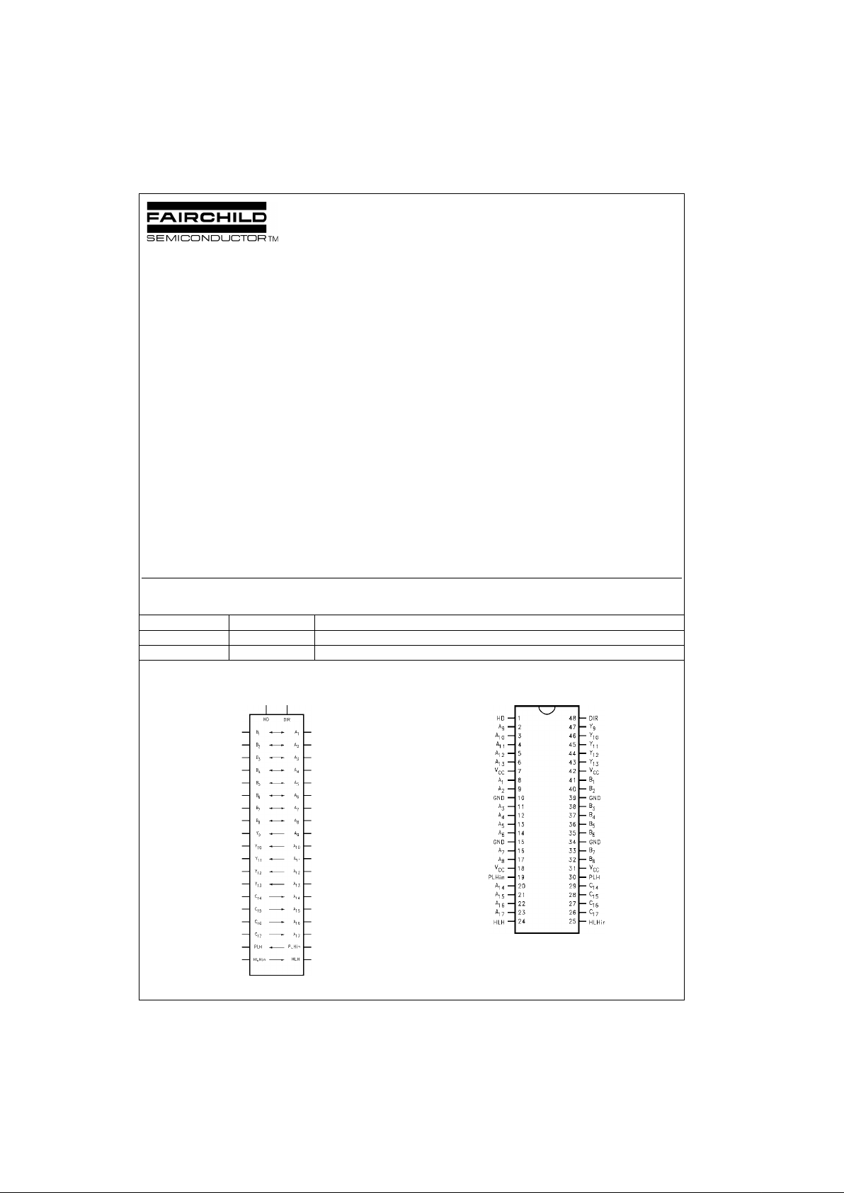
Logic Symbol Connection Diagram
Ordering Number Package Number Package Description
74VHC161284MEA MS48A 48-Lead Small Shrink Outline Package (SSOP), JEDEC MO-118, 0.300 Wide
74VHC161284MTD MTD48 48-Lead Thin Shrink Small Outline Package (TSSOP), JEDEC MO-153, 6.1mm Wide
Page 2
www.fairchildsemi.com 2
74VHC161284
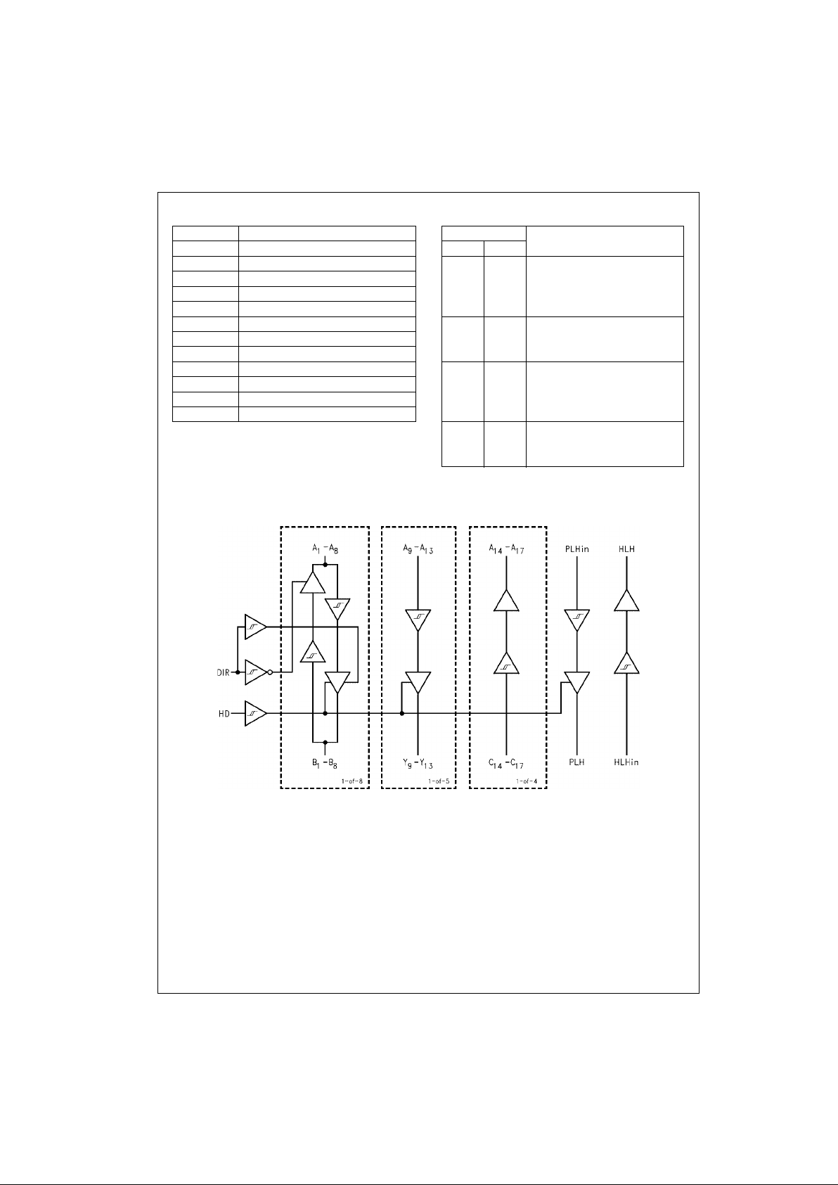
Pin Descriptions Tr uth Table
Note 1: Y9–Y13 Open Drain Outpu ts
Note 2: B
1–B8
Open Drain Outputs
Logic Diagram
Pin Names Description
HD HIGH Drive Enable Input (Active HIGH)
DIR Direction Control Input
A
1–A8
Inputs or Outputs
B
1–B8
Inputs or Outputs
A
9–A13
Inputs
Y
9–Y13
Outputs
A
14–A17
Outputs
C
14–C17
Inputs
PLH
IN
Peripheral Logic HIGH Input
PLH Peripheral Logic HIGH Output
HLH
IN
Host Logic HIGH Input
HLH Host Logic HIGH Output
Inputs
Outputs
DIR HD
LLB
1–B8
Data to A1–A8, and
A
9–A13
Data to Y9–Y13 (Note 1)
C
14–C17
Data to A14–A
17
PLH Open Drain Mode
LHB
1–B 8
Data to A1–A8, and
A
9–A13
Data to Y9–Y
13
C14–C17 Data to A14–A
17
HLA
1–A8
Data to B1–B8 (Note 2)
A
9–A13
Data to Y9–Y13 (Note 1)
C
14–C17
Data to A14–A
17
PLH Open Drain Mode
HHA
1–A8
Data to B1–B
8
A9–A13 Data to Y9–Y
13
C14–C17 Data to A14–A
17
Page 3
3 www.fairchildsemi.com
74VHC161284
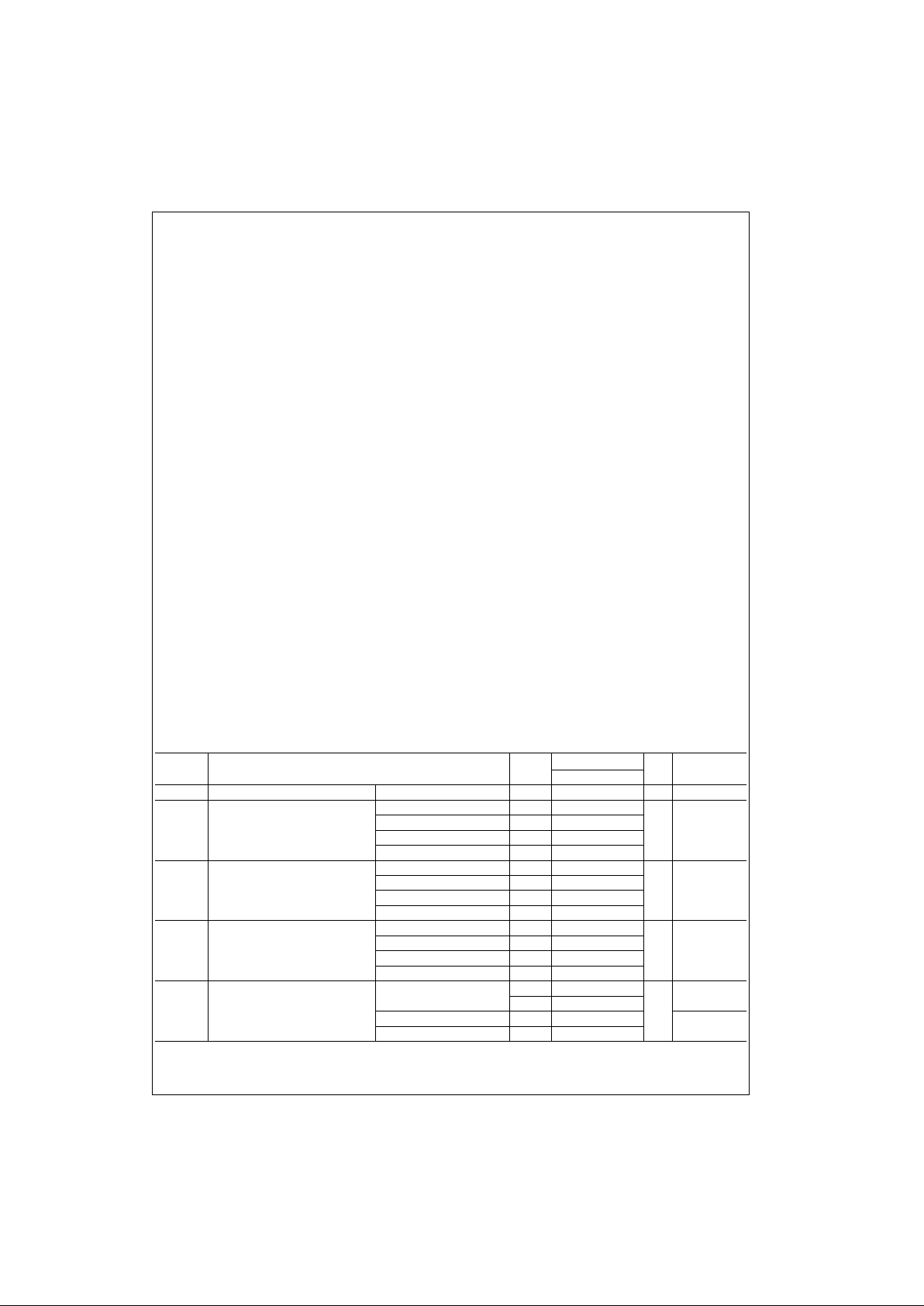
Absolute Maximum Ratings(Note 3) Recommended Operating
Conditions
Note 3: Absolute Maximu m continuos ratings are those values beyond
which damage to the device may occur. Exposure to these indicated may
adversely affect device reliability. Functional operation under absolute maximum rated conditions is not implied.
Note 4: Either voltage lim it or c urrent limit is sufficient to pro te c t in puts.
DC Electrical Characteristics
Supply Voltage
V
CC
−0.5V to + 7.0V
Input Voltage (V
I
) (Note 4)
A
1–A 13
, PLHIN, DIR, HD −0.5V to VCC + 0.5V
B
1–B8
, C14–C17, HLH
IN
−0.5V to + 5.5V (DC)
B
1–B8
, C14–C17, HLH
IN
−2.0V to + 7.0V *
*40 ns Transient
Output Voltage (V
O
)
A
1–A8
, A14–A17, HLH −0.5V to VCC + 0.5V
B
1–B 8
, Y9–Y13, PLH −0.5V to + 5.5V (DC)
B
1–B 8
, Y9–Y13, PLH −2.0V to + 7.0V*
*40 ns Transient
DC Output Current (I
O
)
A
1–A8
, HLH ±25 mA
B
1–B8
, Y9–Y
13
±50 mA
PLH (Output LOW) 84 mA
PLH (Output HIGH) −50 mA
Input Diode Current (I
IK
) (Note 4)
DIR, HD, A
9–A13
,
PLH, HLH, C
14–C17
−20 mA
Output Diode Current (I
OK
)
A
1–A8
, A14–A17, HLH ±50 mA
B
1–B8
, Y9–Y13, PLH −50 mA
DC Continuous V
CC
or
Ground Current
±200 mA
Storage Temperature
−65°C to + 150°C
ESD (HBM) Last Passing
Voltage 2000V
Supply Voltage
V
CC
4.5V to 5.5V
DC Input Voltage (V
I
) 0V to V
CC
Open Drain Voltage (VO) 0V to 5.5V
Operating Temperature (T
A
) −40°C to + 85°C
Symbol Parameter
V
CCTA
= −40°C to +85°C
Units Conditions
(V) Guaranteed Limits
V
IK
Input Clamp Diode Voltage 3.0 −1.2 V II = −18 mA
V
IH
Minimum HIGH Level Input Voltage An, PLHIN, DIR, HD 4.5 − 5.5 0.7 V
CC
V
B
n
4.5 − 5.5 2.0
C
n
4.5 − 5.5 2.3
HLH
IN
4.5 − 5.5 2.6
V
IL
Maximum LOW Level Input Voltage An, PLHIN, DIR, HD 4.5 − 5.5 0.3 V
CC
V
B
n
4.5 − 5.5 0.8
C
n
4.5 − 5.5 0.8
HLH
IN
4.5 − 5.5 1.6
∆VT Minimum Input Hysteresis An, PLHIN, DIR, HD 4.5 − 5.5 0.4
V
V
T
+
–V
T
−
B
n
4.5 − 5.5 0.4 V
T
+
–V
T
−
C
n
5.0 0.8 V
T
+
–V
T
−
HLH
IN
5.0 0.3 V
T
+
–V
T
−
V
OH
Minimum HIGH Level Output Voltage An, HLH 4.5 4.4
V
IOH = −50 µA
4.5 3.8 IOH = −8 mA
Bn, Y
n
4.5 3.73 IOH = −14 mA
PLH 4.5 4.45 IOH = −500 µA
Page 4
www.fairchildsemi.com 4
74VHC161284
DC Electrical Characteristics (Continued)
Note 5: Output impedance is m easured with the output ac t ive LOW and active HIG H (H D = HIGH).
Note 6: This parameter is guaranteed but not tested, characterized only.
Note 7: Power-down leakage t o V
CC
is tested by simultaneously forcing all pins on the cable-side (B1–B8, Y9–Y13, PLH, C14–C17 and HLHIN to 5.5V and
measuring the res ult ing I
CC
.
Symbol Parameter
V
CCTA
= −40°C to +85°C
Units Conditions
(V) Guaranteed Limits
V
OL
Maximum LOW Level Output Voltage An, HLH 4.5 0.1
V
IOL = 50 µA
4.5 0.44 I
OL
= 8 mA
B
n
, Y
n
4.5 0.77 IOL = 14 mA
PLH 4.5 0.7 IOL = 84 mA
RD Maximum Output Impedance B
1–B8
, Y9–Y
13
5.0 55 Ω (Note 5)(Note 6)
Minimum Output Impedance B
1–B8
, Y9–Y
13
5.0 35 Ω (Note 5)(Note 6)
RP Maximum Pull-Up Resistance B1–B8, Y9–Y13, C14–C
17
5.0 1650 Ω
Minimum Pull-Up Resistance B
1–B8
, Y9–Y13, C14–C
17
5.0 1150 Ω
I
IH
Maximum Input Current in HIGH State A9–A13, PLHIN, HD, DIR, HLHIN5.5 1.0
µA
VI = 5.5V
C14–C
17
5.5 100 VI = 5.5V
I
IL
Maximum Input Current in LOW State A9–A13, PLHIN, HD, DIR, HLHIN5.5 −1.0 µAVI = 0.0V
C
14–C17
5.5 −5.0 mA VI = 0.0V
I
OZH
Maximum Output Disable Current A1—A
8
5.5 20
µA
VO = 5.5V
(HIGH) B1–B
8
5.5 100 VO = 5.5V
I
OZL
Maximum Output Disable Current A1—A
8
5.5 −20 µAVO = 0.0V
(LOW) B1–B
8
5.5 −5.0 mA
I
OFF
Power Down Output Leakage B1–B8, Y9–Y13, PLH 0.0 100 µAVO = 5.5V
I
OFF
Power Down Input Leakage C14–C17, HLH
IN
0.0 100 µAVI = 5.5V
I
OFF
− ICCPower Down Leakage to V
CC
0.0 250 µA (Note 7)
I
CC
Maximum Supply Current 5.5 70 mA VI = VCC or GND
Page 5

5 www.fairchildsemi.com
74VHC161284
AC Electrical Characteristics
Note 8: Open Drain
Note 9: t
SKEW
is measured for common edge output transi tions and compares the m easured propagatio n delay for a given path type .
(i) A
1–A8
to B1–B8, A9–Y
13
to Y9–Y
13
(ii) B1–B8 to A1–A
8
(iii) C14–C17 to A14–A
17
Note 10: This parameter is guaranteed but not tested, characterized only.
Capacitance (Note 11)
Note 11: Capacitance is measured at frequ ency = 1 MHz.
Symbol Parameter
T
A
= −40°C to +85°C
Units
Figure
Number
V
CC
= 4.5V − 5.5V
Min Max
t
PHL
A1–A8 to B1–B
8
2.0 30.0 ns Figure 1
t
PLH
A1–A8 to B1–B
8
2.0 30.0 ns Figure 2
t
PHL
B1–B8 to A1–A
8
2.0 30.0 ns Figure 3
t
PLH
B1–B8 to A1–A
8
2.0 30.0 ns Figure 3
t
PHL
A9–A
13
to Y9–Y
13
2.0 30.0 ns Figure 1
t
PLH
A9–A
13
to Y9–Y
13
2.0 30.0 ns Figure 2
t
PHL
C14–C17 to A14–A
17
2.0 30.0 ns Figure 3
t
PLH
C14–C17 to A14–A
17
2.0 30.0 ns Figure 3
t
SKEW
LH-LH or HL-HL 6.0 ns (Note 9)
t
PHL
PLHIN to PLH 2.0 30.0 ns Figure 1
t
PLH
PLHIN to PLH 2.0 30.0 ns Figure 2
t
PHL
HLHIN to HLH 2.0 30.0 ns Figure 3
t
PLH
HLHIN to HLH 2.0 30.0 ns Figure 3
t
PHZ
Output Disable Time 2.0 18.0
ns Figure 7
t
PLZ
DIR to A1–A
8
2.0 18.0
t
PZH
Output Enable Time 2.0 25.0
ns Figure 8
t
PZL
DIR to A1–A
8
2.0 25.0
t
PHZ
Output Disable Time 2.0 25.0
ns Figure 9
t
PLZ
DIR to B1–B
8
2.0 25.0
t
pEN
Output Enable Time
2.0 28.0 ns Figure 2
HD to B1–B8, Y9–Y
13
t
pDis
Output Disable Time
2.0 28.0 ns Figure 2
HD to B
1–B8
, Y9–Y
13
t
pEn–tpDis
Output Enable-Output Disable 20.0 ns
t
SLEW
Output Slew Rate
t
PLH
B1–B8, Y9–Y
13
0.05 0.40
V/ns
Figure 5
t
PHL
0.05 0.40 Figure 4
t
r
, t
f
t
RISE
and t
FALL
120
ns
Figure 6
B
1–B8
, Y9–Y13 (Note 8) 120 (Note 10)
Symbol Parameter Typ Units Conditions
C
IN
Input Capacitance 5 pF VCC = 0.0V (HD, DIR, A9—A13, C14—C17, PLHIN and HLHIN)
C
I/O
I/O Pin Capacitance 12 pF VCC = 3.3V
Page 6

www.fairchildsemi.com 6
74VHC161284
AC Loading and Waveforms
Pulse Generator for all pulses: Rate ≤ 1.0 MHz; ZO ≤ 50Ω; tf ≤ 2.5 ns, tr ≤ 2.5 ns.
FIGURE 1. t
PHL
Test Load and Waveforms
A
1–A8
to B1–B
8
A9–A13 to Y9–Y
13
PLHIN to PLH
FIGURE 2. t
PLH
, t
pEn
, t
pDis
Test Load and Waveforms
A
1–A8
to B1–B8, A9–A13 to Y9–Y
13
PLHIN to PLH, HD to B1–B8, Y9–Y13, PLH
FIGURE 3. t
PHL
, t
PLH
Test Load and Waveforms
B
1–B8
to A1–A8, C14–C17 to A14–A17, HLHIN to HLH
Page 7

7 www.fairchildsemi.com
74VHC161284
AC Loading and Waveforms (Continued)
FIGURE 4. t
SLEW
HL Test Load and Waveforms
A
1–A8
to B1–B
8
A9–A13 to Y9–Y
13
FIGURE 5. t
SLEW
LH Test Load and Waveforms
A
1–A8
to B1–B
8
A9–A13 to Y9–Y
13
tr = Output Rise Time, Open Drain
t
f
= Output Fall Time, Open Dr ain
FIGURE 6. t
RISE
and t
FALL
Test Load and Waveforms for Open Drain Outputs
A
1–A8
to B1–B8, A9–A13 to Y9–Y
13
Page 8

www.fairchildsemi.com 8
74VHC161284
AC Loading and Waveforms (Continued)
FIGURE 7. t
PHZ
and t
PLZ
Test Load and Waveforms, DIR to A1–A
8
FIGURE 8. t
PZH
and t
PZL
Test Load and Waveforms, DIR to A1–A
8
Page 9

9 www.fairchildsemi.com
74VHC161284
AC Loading and Waveforms (Continued)
FIGURE 9. t
PHZ
and t
PLZ
Te st Load and Waveforms, DIR to B1–B
8
Page 10

www.fairchildsemi.com 10
74VHC161284
Physical Dimensions inches (millimeters) unless otherwise noted
48-Lead Small Shrink Outline Package (SSOP), JEDEC MO-118, 0.300 Wide
Package Number MS48A
Page 11

11 www.fairchildsemi.com
74VHC161284 IEEE 1284 Transceiver
Physical Dimensions inches (millimeters) unless otherwise noted (Continued)
48-Lead Thin Shrink Sm all Ou tline Pa ck age (TS SO P), JE DE C MO-153, 6.1mm Wide
Package Number MTD48
Fairchild does not assume any responsibility for use of any circuitry described , no circuit patent licenses are implied and
Fairchild reserves the right at any time without notice to change said circuitry and specifications.
LIFE SUPPORT POLICY
FAIRCHILD’S PRODUCTS ARE NOT AUTHORIZED FOR USE AS CRITICAL COMPONENTS IN LIFE SUPPORT
DEVICES OR SYSTEMS WITHOUT THE EXPRESS WRITTEN APPROVAL OF THE PRESIDENT OF FAIRCHILD
SEMICONDUCTOR CORPORATION. As used herein:
1. Life support devices or systems are dev ic es or syste ms
which, (a) are intended for surgical implant into the
body, or (b) support or sustain life, and (c) whose failure
to perform when properly used in accordance with
instructions for use provide d in the labe l ing, can be re asonably expected to result in a significant injury to the
user.
2. A critical compo nent in any com ponen t of a life s upp ort
device or system whose failure to perform can be reasonably expected to cause the failure of the l ife support
device or system, or to affect its safety or effectiveness.
www.fairchildsemi.com
 Loading...