

Page 1
查询74V2T04供应商
74V2T04
TRIPLE INVERTER
■ HIGH SPEED: t
■ LOW POWER DISSIPATION:
I
=1µA(MAX.) atTA=25°C
CC
■ COMPATIBLE WITHTTL OUTPUTS:
V
=2V(MIN),VIL=0.8V(MAX)
IH
■ POWER DOWN PROT ECTION ON INPUT
■ SYMMETRICAL OUTPUT IMPEDANCE:
|I
|=IOL=8mA(MIN)atVCC=4.5V
OH
■ BALANCED PROPAGATION DELAYS:
t
≅ t
PLH
PHL
■ OPERATING VOLTAGE RANG E:
V
(OPR) = 4.5V to 5.5V
CC
■ IMPROVED LATCH-UP IMMUNITY
= 4.7ns (TYP.) at VCC=5V
PD
DESCRIPTION
The 74V2T04 is an advanced high-speed CMOS
TRIPLE INVERTER fabricated with sub-micron
silicon gate and double-layer me tal wiring C
2
MOS
technology.
SOT23-8L
ORDER CODES
PACKAGE T & R
SOT23-8L 74V2T04STR
The internal circuit i s composed of 3 stages
including buffer output, which provide high noise
immunity and stable output.
Power down protection is prov ided on input and 0
to 7V c an be accepted on input with no regard t o
the supply voltage. This device can be used to
interface5Vto3V.
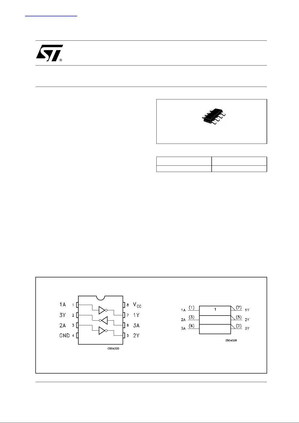
PIN CONNECTION AND IEC LOGIC SYMBOLS
1/7June 2003
Page 2
74V2T04
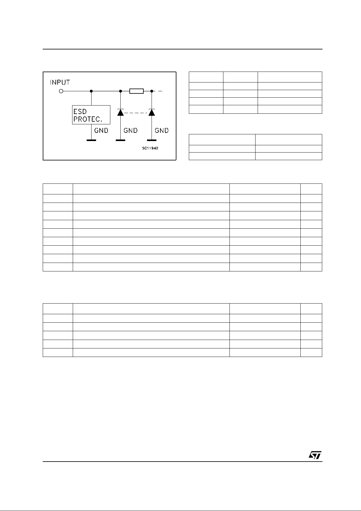
INPUT EQUIVALENT CIRCUIT PIN DESCRIPTION
PIN N° SYMBOL NAME QND FUNCTION
1, 3, 6 1A, 2A, 3A Data Inputs
7, 5, 2 1Y, 2Y, 3Y Data Outputs
4 GND Ground (0V)
8
TRUTH TABLE
ABSOLUTE MAXIMUM RATINGS
Symbol Parameter Value Unit
V
V
V
I
I
OK
I
I
or I
CC
T
T
Absolute Maximum Ratings are those values beyond which damage to the device may occur. Functional operation under these conditions is
not implied
Supply Voltage
CC
DC Input Voltage
I
DC Output Voltage -0.5 to VCC+ 0.5
O
DC Input Diode Current
IK
DC Output Diode Current
DC Output Current
O
DC VCCor Ground Current
GND
Storage Temperature
stg
Lead Temperature (10 sec)
L
V
CC
Positive Supply Voltage
AY
LH
HL
-0.5 to +7.0 V
-0.5 to +7.0 V
V
-20 mA
± 20 mA
± 25 mA
± 50 mA
-65 to +150 °C
300 °C
RECOMMENDED OPERATING CONDITIONS
Symbol Parameter Value Unit
V
V
V
T
dt/dv
1) VINfrom0.8V to 2V
2/7
Supply Voltage
CC
Input Voltage
I
Output Voltage 0 to V
O
Operating Temperature
op
Input Rise and Fall Time (note 1) (V
=5.0±0.5V)
CC
4.5 to 5.5 V
0 to 5.5 V
CC
-55 to 125 °C
0 to 20 ns/V
V
Page 3
DC SPECIFICATIONS
Symbol Parameter
V
V
V
+
High Level Input
IH
Voltage
V
Low Level Input
IL
Voltage
High Level Output
OH
Voltage
Low Level Output
OL
Voltage
Input Leakage
I
I
Current
Quiescent Supply
I
CC
Current
I
Additional Worst
CC
Case Supply
Current
Test Condition Value
= 25°C
T
V
CC
(V)
4.5to
A
Min. Typ. Max. Min. Max. Min. Max.
222V
5.5
4.5to
5.5
4.5
4.5
4.5
4.5
0to
5.5
5.5
IO=-50 µA 4.4 4.5 4.4 4.4 V
=-8 mA 3.94 3.8 3.7
I
O
IO=50 µA 0.0 0.1 0.1 0.1 V
=8 mA 0.36 0.44 0.55
I
O
VI= 5.5V or GND
V
I=VCC
or GND
One Input at 3.4V,
other input at V
5.5
CC
or GND
74V2T04
-40 to 85°C -55 to 125°C
0.8 0.8 0.8 V
± 0.1 ± 1.0 ± 1.0 µA
11020µA
1.35 1.5 1.5 mA
Unit
AC ELECTRICAL CHARACTERISTICS (Input t
r=tf
=3ns)
Test Condition Value
Symbol Parameter
t
t
(*) Voltage range is5.0V ± 0.5V
Propagation Delay
PLH
Time
PHL
T
V
CC
(V)
C
(pF)
L
A
Min. Typ. Max. Min. Max. Min. Max.
5.0 (*) 15 4.7 6.7 1.0 7.5 1.0 8.5
5.0 (*) 50 5.5 7.7 1.0 8.5 1.0 9.5
-40 to 85°C -55 to 125°C
Unit
ns
= 25°C
CAPACITIVE CHARACTERISTICS
Test Condition Value
= 25°C
Symbol Parameter
T
A
Min. Typ. Max. Min. Max. Min. Max.
C
C
Input Capacitance
IN
Power Dissipation
PD
Capacitance
410 10 10pF
16 pF
(note 1)
1) CPDis defined as the value of the IC’s internal equivalent capacitance which is calculated from the operating current consumption without
load. (Refer to Test Circuit). Average operating current can be obtained by the following equation. I
-40 to 85°C -55 to 125°C
CC(opr)=CPDxVCCxfIN+ICC
Unit
/3
3/7
Page 4

74V2T04
TEST CIRCUIT
CL=15/50pF or equivalent (includes jig and probe capacitance)
R
T=ZOUT
WAVEFORM: PROPAGATION DELAY (f=1MHz; 50% duty cycle)
of pulse generator (typically 50Ω)
4/7
Page 5

74V2T04
SOT23-8L MECHANICAL DATA
mm. mils
DIM.
MIN. TYP MAX. MIN. TYP. MAX.
A 0.90 1.45 35.4 57.1
A1 0.00 0.15 0.0 5.9
A2 0.90 1.30 35.4 51.2
b 0.22 0.38 8.6 14.9
C 0.09 0.20 3.5 7.8
D 2.80 3.00 110.2 118.1
E 2.60 3.00 102.3 118.1
E1 1.50 1.75 59.0 68.8
e0.65 25.6
e1 1.95 76.7
L 0.35 0.55 13.7 21.6
5/7
Page 6

74V2T04
Tape & Reel SOT23-xL MECHANICAL DATA
DIM.
MIN. TYP MAX. MIN. TYP. MAX.
A 180 7.086
C 12.8 13.0 13.2 0.504 0.512 0.519
D 20.2 0.795
N 60 2.362
T 14.4 0.567
Ao 3.13 3.23 3.33 0.123 0.127 0.131
Bo 3.07 3.17 3.27 0.120 0.124 0.128
Ko 1.27 1.37 1.47 0.050 0.054 0.0.58
Po 3.9 4.0 4.1 0.153 0.157 0.161
P 3.9 4.0 4.1 0.153 0.157 0.161
mm. inch
6/7
Page 7

74V2T04
Information furnished is believed to be accurate and reliable. However, STMicroelectronics assumes no responsibility for the
consequences of use o f suc h inf ormat ion n or f or an y infr ingeme nt of paten ts or oth er ri gh ts of third part ies whic h may resul t f rom
its use. No license is granted by implication or otherwise under any patent or patent rights of STMicroelectronics. Specifications
mentioned in this publication are subject to change without notice. This publication supersedes and replaces all information
previously supplied. STMicroelectronics products are not authorized for use as critical components in life support devices or
systems without express written approval of STMicroelectronics.
Australia - Brazil - Canada - China - Finland - France - Germany - Hong Kong - India - Israel - Italy - Japan - Malaysia - Malta - Morocco
© The ST logo is a registered trademark of STMicroelectronics
© 2003 STMicroelectronics - Printed in Italy - All Rights Reserved
STMicroelectronics GROUP OF COMPANIES
Singapore - Spain - Sweden - Switzerland - United Kingdom - United States.
© http://www.st.com
7/7
Page 8

WWW.ALLDATASHEET.COM
Copyright © Each Manufacturing Company.
All Datasheets cannot be modified without permission.
This datasheet has been download from :
www.AllDataSheet.com
100% Free DataSheet Search Site.
Free Download.
No Register.
Fast Search System.
www.AllDataSheet.com
 Loading...