

Page 1
查询74V2G70CTR供应商
SINGLE D-TYPE FLIP FLOP WITH PRESET AND CLEAR
74V2G74
■ HIGH SPEED:
f
= 170 MHz (TYP.) at VCC = 5V
MAX
■ LOW POWER DISSIPATION:
I
= 1 µA (MAX.) at TA=25°C
CC
■ HIGH NOISE IMMUNITY:
V
= V
NIH
■ POWER DOWN PROTECTION ON INPUTS
■ SYMMETRICAL OUTPUT IMPEDANCE:
|I
| = IOL = 8 mA (MIN)
OH
■ BALANCED PROPAGATION DELAYS:
t
≅ t
PLH
■ OPERATING VOLTAGE RANGE:
V
(OPR) = 2V to 5.5V
CC
■ FUNCTION COMPATIBLE WITH
= 28% VCC (MIN.)
NIL
PHL
74 SERIES 74
■ IMPROVED LATCH-UP IMMUNITY
DESCRIPTION
The 74V2G74 is an advanced high-speed CMOS
SINGLE D-TYPE FLIP FLOP WITH PRESET
AND CLEAR fabricated with sub-micron silicon
gate and double-layer metal wiring C
2
MOS
tecnology.
A signal on the D INPUT is transfered to the Q and
Q
OUTPUTS during the positive going transition
of the clock pulse.
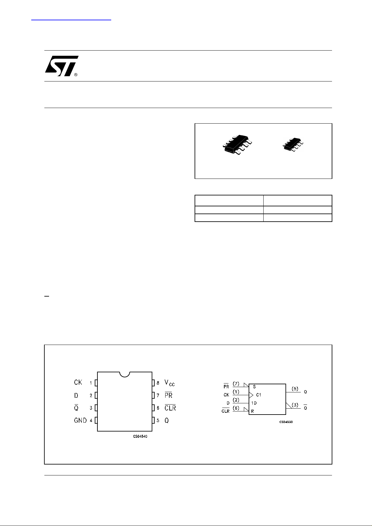
SOT23-8L SOT323-8L
ORDER CODES
PACKAGE T & R
SOT23-8L 74V2G70STR
SOT323-8L 74V2G70CTR
CLEAR and PRESET are independent of the
clock and accomplished by a low setting on the
appropriate input.
Power down protection is provided on all inputs
and 0 to 7V can be accepted on inputs with no
regard to the supply voltage. This device can be
used to interface 5V to 3V.
All inputs and outputs are equipped with
protection circuits against stat ic discharge, giving
them ESD immunity and transient excess voltage.
PIN CONNECTION AND IEC LOGIC SYMBOLS
1/13December 2001
Page 2
74V2G74
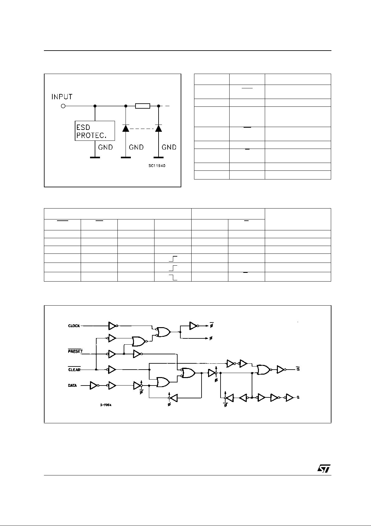
INPUT EQUIVALENT CIRCUIT PIN DESCRIPTION
PIN No SYMBOL NAME AND FUNCTION
6CLR
2 D Data Input
1 CK Clock Input
7PR
5 Q True Flip-Flop Output
3Q
4 GND Ground (0V)
8V
TRUTH TABLE
CC
Asyncronous Reset Direct Input
(LOW to HIGH, Edge
Triggered)
Asyncronous Set - Direct
Input
Complement Flip-Flop
Output
Positive Supply Voltage
INPUTS OUTPUTS
CLR
PR DCKQ Q
L H X X L H CLEAR
H L X X H L PRESET
LLXXHH
HHL LH
HHH HL
HHX
X= Don’t care
Q
n
Q
n
LOGIC DIAGRAM
FUNCTION
NO CHANGE
This log i c diagram has not be used to esti m ate propagation delays
2/13
Page 3
74V2G74
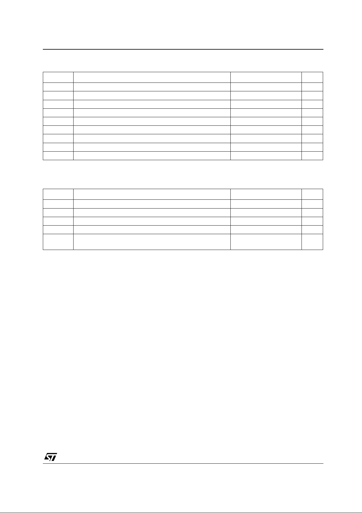
ABSOLUTE MAXIMUM RATINGS
Symbol Parameter Value Unit
V
V
V
I
I
OK
I
I
or I
CC
T
T
Absolute Maximum Ratings are those values beyond which damage to the device may occur. Functional operation under these conditions is
not implied
RECOMMENDED OPERATING CONDITIONS
Symbol Parameter Value Unit
V
V
V
T
dt/dv
1) VIN from 30 % to 70% of V
Supply Voltage
CC
DC Input Voltage
I
DC Output Voltage -0.5 to VCC + 0.5
O
DC Input Diode Current
IK
DC Output Diode Current
DC Output Current
O
DC VCC or Ground Current
GND
Storage Temperature
stg
Lead Temperature (10 sec)
L
Supply Voltage
CC
Input Voltage
I
Output Voltage 0 to V
O
Operating Temperature
op
Input Rise and Fall Time (note 1) (V
(V
CC
= 3.3 ± 0.3V)
CC
= 5.0 ± 0.5V)
CC
-0.5 to +7.0 V
-0.5 to +7.0 V
− 20 mA
− 20 mA
± 25 mA
± 50 mA
-65 to +150 °C
300 °C
2 to 5.5 V
0 to 5.5 V
CC
-55 to 125 °C
0 to 100
0 to 20
ns/V
V
V
3/13
Page 4
74V2G74
DC SPECIFICATIONS
Symbol Parameter
V
V
V
V
I
High Level Input
IH
Voltage
Low Level Input
IL
Voltage
High Level Output
OH
Voltage
Low Level Output
OL
Voltage
I
Input Leakage
I
Current
Quiescent Supply
CC
Current
Test Condition Value
V
(V)
CC
= 25°C
A
Min. Typ. Max. Min. Max. Min. Max.
-40 to 85°C -55 to 125°C
T
2.0 1.5 1.5 1.5
3.0 to
5.5
0.7V
CC
0.7V
CC
0.7V
CC
2.0 0.5 0.5 0.5
3.0 to
5.5
2.0
3.0
4.5
3.0
4.5
2.0
3.0
4.5
3.0
4.5
0 to
5.5
5.5
=-50 µA
I
O
I
=-50 µA
O
I
=-50 µA
O
I
=-4 mA
O
I
=-8 mA
O
IO=50 µA
I
=50 µA
O
I
=50 µA
O
I
=4 mA
O
I
=8 mA
O
V
= 5.5V or GND
I
= VCC or GND
V
I
1.9 2.0 1.9 1.9
2.9 3.0 2.9 2.9
4.4 4.5 4.4 4.4
2.58 2.48 2.4
3.94 3.8 3.7
0.3V
CC
0.3V
CC
0.0 0.1 0.1 0.1
0.0 0.1 0.1 0.1
0.0 0.1 0.1 0.1
0.36 0.44 0.55
0.36 0.44 0.55
± 0.1 ± 1 ± 1 µA
22020µA
0.3V
CC
Unit
V
V
V
V
4/13
Page 5
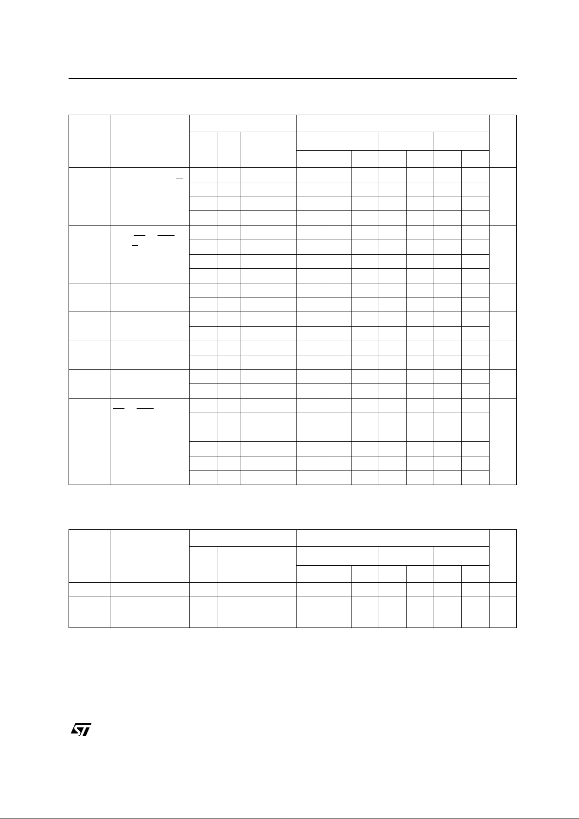
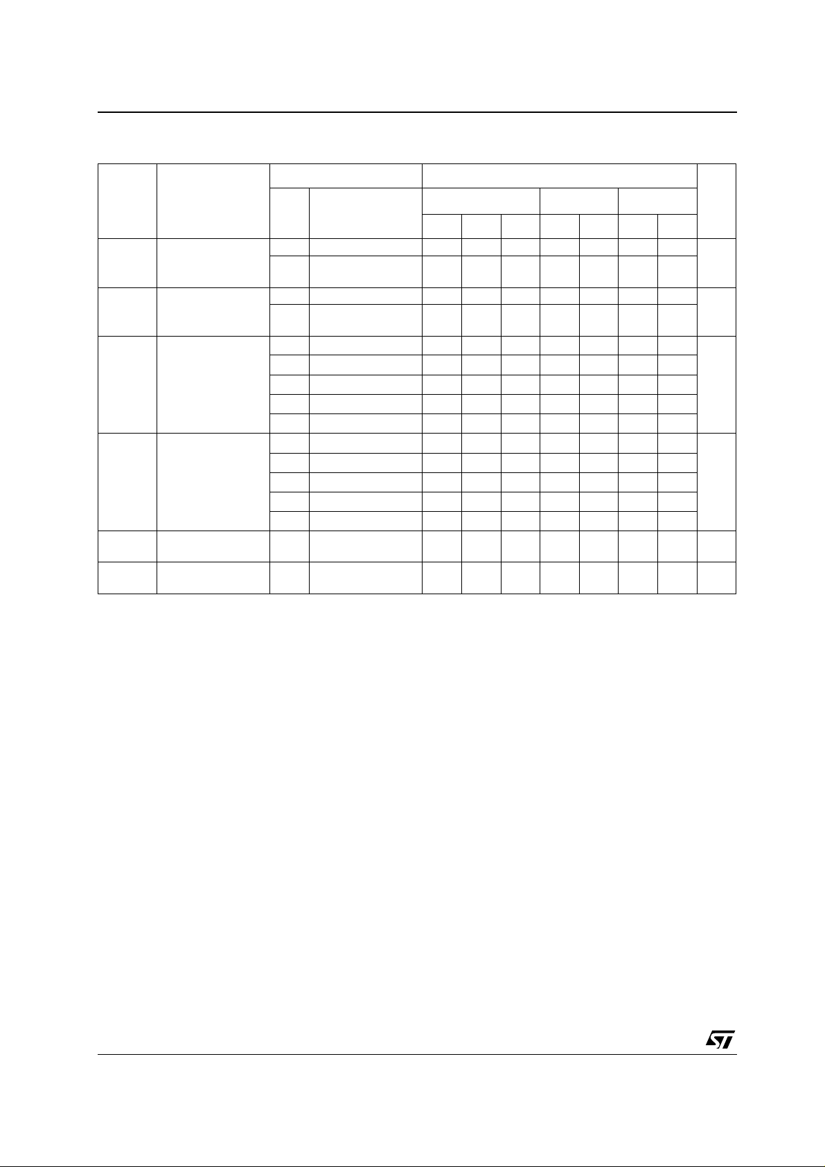
AC ELECTRICAL CHARACTERISTICS (Input tr = tf = 3ns)
Test Condition Value
T
Symbol Param eter
t
Propagation Delay
PLH
t
t
t
Time CK to Q or Q
PHL
Propagation Delay
PLH
Time PR
PHL
Q or Q
CK Pulse Width
t
W
HIGH or LOW
t
W
PR or CLR Pulse
or CLR to
Width LOW
Setup Time D to CK
t
s
HIGH or LOW
Hold Time D to CK
t
h
HIGH or LOW
t
REM
f
MAX
(*) Vol tage range is 3.3V ± 0.3V
(**) Voltage range is 5.0V ±
Removal Time
or CLR to CK
PR
Maximum Clock
Frequency
0.5V
V
3.3
3.3
5.0
5.0
3.3
3.3
5.0
5.0
3.3
5.0
3.3
5.0
3.3
5.0
3.3
5.0
3.3
5.0
3.3
3.3
5.0
5.0
C
CC
(V)
L
(pF)
(*)
15 6.7 11.9 1.0 14.0 1.0 14.0
(*)
50 9.2 15.4 1.0 17.5 1.0 17.5
(**)
15 4.6 7.3 1.0 8.5 1.0 8.5
(**)
50 6.1 9.3 1.0 10.5 1.0 10.5
(*)
15 7.6 12.3 1.0 14.5 1.0 14.5
(*)
50 10.1 15.8 1.0 18.0 1.0 18.0
(**)
15 4.8 7.7 1.0 9.0 1.0 9.0
(**)
50 6.3 9.7 1.0 11.0 1.0 11.0
(*)
(**)
(*)
(**)
(*)
(**)
(*)
(**)
(*)
(**)
(*)
15 80 125 70 70
(*)
50 50 75 45 45
(**)
15 130 170 110 110
(**)
50 90 115 75 75
= 25°C
A
Min. Typ. Max. Min. Max. Min. Max.
6.0 7.0 7.0
5.0 5.0 5.0
6.0 7.0 7.0
5.0 5.0 5.0
6.0 7.0 7.0
5.0 5.0 5.0
0.5 0.5 0.5
0.5 0.5 0.5
5.0 5.0 5.0
3.0 3.0 3.0
74V2G74
-40 to 85°C -55 to 125°C
Unit
ns
ns
ns
ns
ns
ns
ns
MHz
CAPACITIVE CHARACTERISTICS
Test Condition Value
T
Symbol Parameter
V
CC
(V)
C
C
Input Capacitance
IN
Power Dissipation
PD
Capacitance
3.3 4101010pF
= 10MHz
3.3
f
IN
(note 1)
1) CPD is defined as the value of the IC’s internal equivalent capacitance which is calculated from the operating current consumption without
load. (R ef er to Test Circ ui t). Averag e operatin g current can be obtained by t he following equation. I
= 25°C
A
-40 to 85°C -55 to 125°C
Min. Typ. Max. Min. Max. Min. Max.
22 pF
= CPD x VCC x fIN + I
CC(opr)
CC
Unit
5/13
Page 6

74V2G74
TEST CIRCUIT
CL =15/50pF or equivalent (i ncludes jig and probe capacitance)
R
= Z
of pulse generator (typically 50Ω)
T
OUT
WAVEFORM 1: PROPAGATION DELAYS, SETUP AND HOLD TIMES (D TO CK), CK MAXIMUM
FREQUENCY , CK MINIMUM PULSE WIDTH (f=1MHz; 50% duty cycle)
6/13
Page 7

74V2G74
WAVEFORM 2: PROPAGATION DELAYS MINIMUM PULSE WIDTH (CLR AND PR) (f=1MHz; 50%
duty cycle)
WAVEFORM 3: RECOVERY TIME (f=1MHz; 50% duty cycle)
7/13
Page 8

74V2G74
WAVEFORM 4: PULSE WIDTHS
8/13
Page 9

74V2G74
SOT23-8L MECHANICAL DATA
mm. mils
DIM.
MIN. TYP MAX. MIN. TYP. MAX.
A 0.90 1.45 35.4 57.1
A1 0.00 0.15 0.0 5.9
A2 0.90 1.30 35.4 51.2
b 0.22 0.38 8.6 14.9
C 0.09 0.20 3.5 7.8
D 2.80 3.00 110.2 118.1
E 2.60 3.00 102.3 118.1
E1 1.50 1.75 59.0 68.8
e0.65 25.6
e1 1.95 76.7
L 0.35 0.55 13.7 21.6
9/13
Page 10

74V2G74
SOT323-8L MECHANICAL DATA
mm. mils
DIM.
MIN. TYP MAX. MIN. TYP. MAX.
A 0.80 1.10 31.5 43.3
A1 0.00 0.10 0.0 3.9
A2 0.80 1.00 31.5 34.9
b 0.13 0.28 5.1 11.0
C 0.10 0.18 3.9 7.1
D 1.80 2.20 70.9 86.6
E 1.80 2.40 70.9 94.5
E1 1.15 1.35 45.3 53.1
e 0.5 19.7
e1 1.5 59.0
L 0.10 0.30 3.9 11.8
10/13
Page 11

Tape & Reel SOT23-xL MECHANICAL D ATA
74V2G74
DIM.
MIN. TYP MAX. MIN. TYP. MAX.
A 180 7.086
C 12.8 13.0 13.2 0.504 0.512 0.519
D 20.2 0.795
N 60 2.362
T 14.4 0.567
Ao 3.13 3.23 3.33 0.123 0.127 0.131
Bo 3.07 3.17 3.27 0.120 0.124 0.128
Ko 1.27 1.37 1.47 0.050 0.054 0.0.58
Po 3.9 4.0 4.1 0.153 0.157 0.161
P 3.9 4.0 4.1 0.153 0.157 0.161
mm. inch
11/13
Page 12

74V2G74
Tape & Reel SOT323-xL MECHANICAL DATA
DIM.
MIN. TYP MAX. MIN. TYP. MAX.
A 175 180 185 6.889 7.086 7.283
C 12.8 13 13.2 0.504 0.512 0.519
D 20.2 0.795
N 59.5 60 60.5 2.362
T 14.4 0.567
Ao 2.25 0.088
Bo 2.7 0.106
Ko 1.2 0.047
Po 3.98 4 4.2 0.156 0.157 0.165
P 3.98 4 4.2 0.156 0.157 0.165
mm. inch
12/13
Page 13

74V2G74
Information furnished is believed to be accurate and reliable. H owever, STMicroelectronics assumes no responsibility f or t he
consequences of use of such informatio n nor for any infringement of paten ts or o ther rig hts of t hird part ies which ma y result from
its use. No license is granted by implication or otherwise under any patent or patent rights of STMicroelectronics. Specifications
mentioned in this publicatio n are subject to change without notice. This publication supersedes and replaces all information
previousl y suppl ied. STM icroel ectronics produc ts are not auth orized for use as c ritica l compone nts in l ife s upport dev ices or
systems without express written approval of STMicroelectronics.
Australia - Brazil - Canada - China - Finland - France - Germany - Hong Kong - India - Israel - Italy - Japan - Malaysia - Malta - Morocco
© The ST logo is a registered trademark of STMicroelectronics
© 2001 STMicroelectronics - Printed in Italy - All Rights Reserved
STMicroelectronics GROUP OF COMPANIES
Singapore - Spain - Sweden - Switzerland - United Kingdom - United States.
© http://www.st.com
13/13
Page 14

WWW.ALLDATASHEET.COM
Copyright © Each Manufacturing Company.
All Datasheets cannot be modified without permission.
This datasheet has been download from :
www.AllDataSheet.com
100% Free DataSheet Search Site.
Free Download.
No Register.
Fast Search System.
www.AllDataSheet.com
 Loading...