

Datasheet 74LVXC4245TTR, 74LVXC4245MTR, 74LVXC4245M Datasheet (SGS Thomson Microelectronics)
Page 1
74LVXC4245
OCTAL DUAL SUPPLY BUS TRANSCEIVER
■ HIGH SPEED:
t
= 6.5ns (MAX.) at
PD
V
= 5.0V, V
CCA
■ LOW POWER DISSIPATION:
I
= I
CCA
■ LOW NOISE: V
V
CCA
■ SYMMETRICAL OUTPUT IMPEDANCE:
|I
| = IOL = 24mA (MIN)
OH
■ BALANCED PROPAGATION DELAYS:
t
≅ t
PLH
■ OPERATING VOLTAGE RANGE:
V
CCA
V
CCB
= 5µA(MAX.) at TA=25°C
CCB
=5.0V V
PHL
(OPR) = 4.5V to 5.5V (1.2V Data Retention)
(OPR) = 2.7V to 5.5V (1.2V Data Retention)
= 5.0V
CCB
=0.3V (TYP.) at
OLP
=3.3V
CCB
PIN AND FUNCTION COMPATIBLE WITH
74 SERIES C4245
■ IMPROVED LATCH-UP IMMUNITY
DESCRIPTION
The 74LVXC4245 is a dual supply 8 bit
configurable low voltage CMOS OCTAL BUS
TRANSCEIVER fabricated with sub-micron silicon
gate and double-layer metal wiring C
2
MOS
technology. Designed for use as an interface
between a 5V bus and a 3.3V to 5V bus in a mixed
5V/3.3V supply systems, it achieves high speed
operation while m aintaining t he CM OS l ow p ower
dissipation.
TSSOPSOP
ORDER CODES
PACKAGE TUBE T & R
SOP 74LVXC4245M 74LVXC4245MTR
TSSOP 74LVXC4245TTR
This IC is intended for two-way asynchronous
communication between data buses and the
direction of data transmission is determined by
DIR input. The enable input G
can be used to
disable the device so that the buses are effectively
isolated.
The A-port interfaces with the 5V bus, the B-port
with the 3.3V to 5V bus.
All inputs are equipped with protection circuits
against static discharge, giving them 2KV ESD
immunity and transient excess voltage.
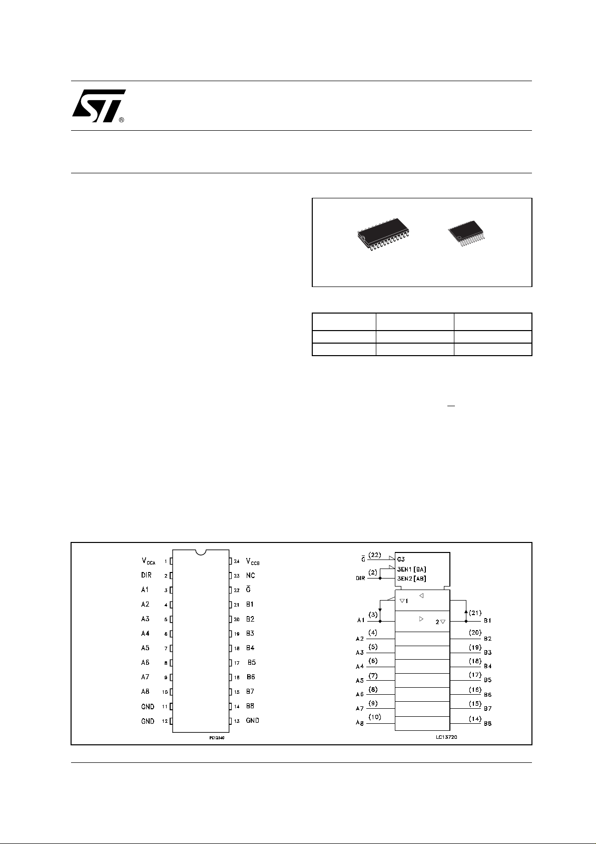
PIN CONNECTION AND IEC LOGIC SYMBOLS
1/11July 2001
Page 2
74LVXC4245
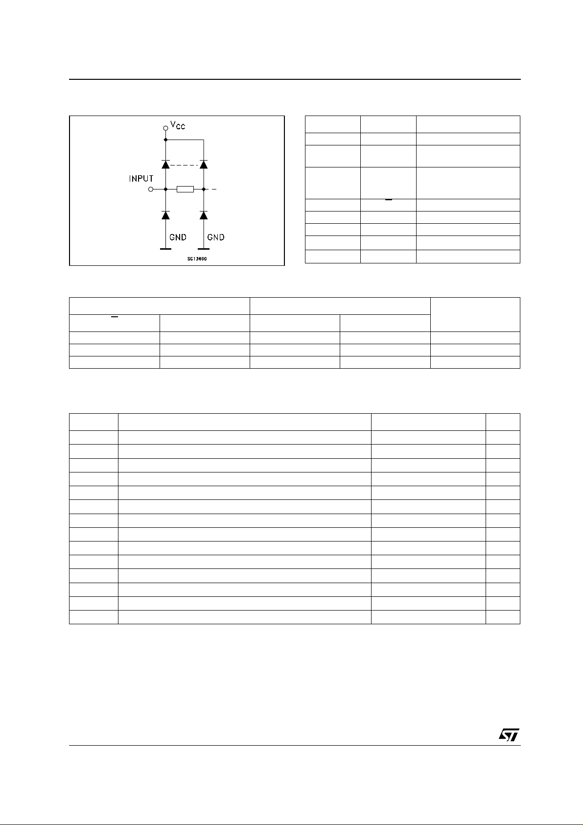
INPUT AND OUTPUT EQUIVALENT CIRCUIT PIN DESCRIPTION
PIN No SYMBOL NAME AND FUNCTION
2 DIR Directional Control
3, 4, 5, 6, 7,
8, 9, 10
21, 20, 19,
18, 17, 16,
15, 14
22 G
11, 12, 13 GND Ground (0V)
23 NC Not Connected
1V
24 V
TRUTH TABLE
A1 to A8 Data Inputs/Outputs
B1 to B8 Data Inputs/Outputs
CCA
CCB
Output Enable Input
Positive Supply Voltage
Positive Supply Voltage
INPUTS FUNCTION
OUTPUT
G
DIR A BUS B BUS
L L OUTPUT INPUT A = B
L H INPUT OUTPUT B = A
HXZZZ
X : Don’t Care
Z : High Impedance
ABSOLUTE MAXIMUM RATINGS
Symbol Parameter Value Unit
V
CCA
V
CCB
V
V
I/OA
V
I/OB
I
I
OK
I
OA
I
OB
I
CCA
I
CCB
P
T
T
Absolute Maximum Ratings are those values beyond which damage to the device may occur. Functional operation under these conditions is
not implied
Supply Voltage
Supply Voltage
DC Input Voltage -0.5 to V
I
DC I/O Voltage -0.5 to V
DC I/O Voltage -0.5 to V
DC Input Diode Current
IK
DC Output Diode Current
DC Output Current
DC Output Current
DC VCC or Ground Current
DC VCC or Ground Current
Power Dissipation
d
Storage Temperature
stg
Lead Temperature (10 sec)
L
-0.5 to +7.0 V
-0.5 to +7.0 V
+ 0.5
CCA
+ 0.5
CCA
+ 0.5
CCB
± 20 mA
± 50 mA
± 50 mA
± 50 mA
± 200 mA
± 100 mA
180 mW
-65 to +150 °C
300 °C
V
V
V
2/11
Page 3
74LVXC4245
RECOMMENDED OPERATING CONDITIONS
Symbol Parameter Value Unit
V
CCA
V
CCB
V
V
I/OA
V
I/OB
T
dt/dv Input Rise and Fall Time (note 2) 0 to 10 ns/V
1) VIN from 30 % to 70% of V
2) V
CCA
Supply Voltage (note 1)
Supply Voltage (note 1)
Input Voltage 0 to V
I
I/O Voltage 0 to V
I/O Voltage 0 to V
Operating Temperature
op
= 4.5 to 5.5V; V
CC
= 2.7 to 3.6V;
CCB
4.5 to 5.5 V
2.7 to 5.5 V
CCA
CCA
CCB
-40 to 85 °C
V
V
V
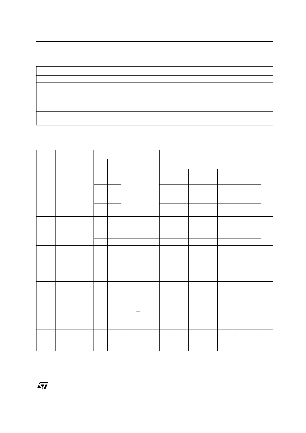
DC SPECIFICATIONS FOR V
Symbol Parameter
V
V
V
I
High Level Input
IHA
Voltage
Low Level Input
V
ILA
Voltage
High Level
OHA
Output Voltage
Low Level Output
OLA
Voltage
I
Input Leakage
IA
Current
High Impedance
OZA
Output Leakage
Current
I
I
CCtAF
Quiescent Supply
CCtA
Current
Quiescent V
Supply Current
as B Port Floats
∆I
Maximum
CCtA
Quiescent Supply
Current / Input
(An, DIR, G
CCA
)
V
CCA
(V)
4.5 2.7 2.0 2.0 2.0
5.5 5.5 2.0 2.0 2.0
4.5 2.7 0.8 0.8 0.8
5.5 5.5 0.8 0.8 0.8
4.5 3.0
4.5 3.0
4.5 3.0
4.5 3.0
5.5 3.6
5.5 3.6 VIA = V
5.5 3.6 VIA = V
5.5 Open VIA = V
5.5 5.5 V
CCA
Test Condition Value
T
= 25 °C
V
CCB
(V)
IO=-100 µA
I
=-24 mA
O
IO=100 µA
=24 mA
I
O
V
= VCC or GND
I
or V
IHA
VIB = V
V
I/OA
IHB
= V
or V
CCA
ILA
ILB
or
A
Min. Typ. Max. Min. Max. Min. Max.
4.4 4.5 4.4 4.4
3.86 3.76 3.76
0 0.1 0.1 0.1
0.36 0.44 0.44
± 0.1 ± 1 ± 1 µA
± 0.5 ± 5 ± 5 µA
GND
CCA
or
55050µA
GND
V
IB
= V
CCB
or
GND
55050µA
GND G
V
CCA
= DIR =
CCA
or
VIB = Open
IA
V
= V
IB
= V
CCA
- 2.1V
CCB
or
1.35 1.5 1.5 mA
GND
-40 to 85 °C -55 to 125°C
Unit
V4.5 3.6 2.0 2.0 2.0
V4.5 3.6 0.8 0.8 0.8
V
V
3/11
Page 4
74LVXC4245
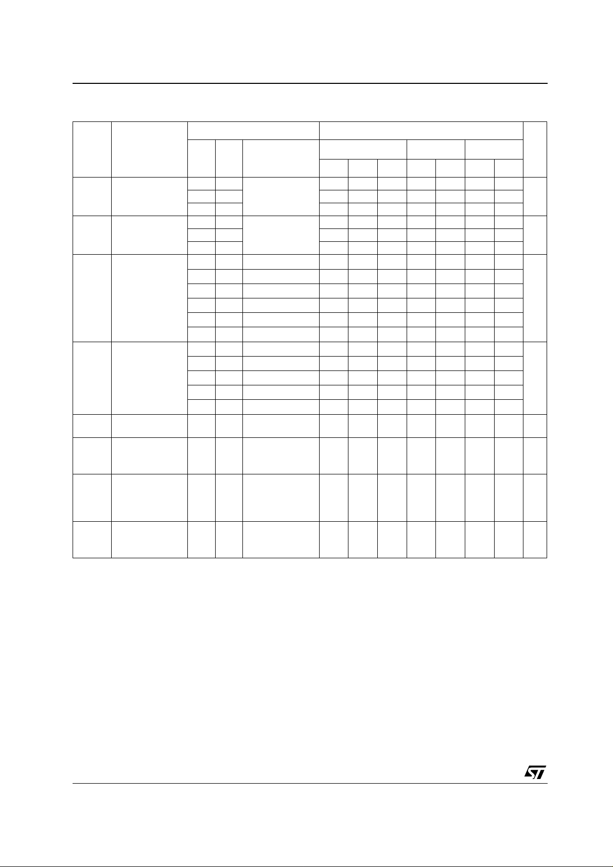
DC SPECIFICATIONS FOR V
Symbol Parameter
V
V
V
I
High Level Input
IHB
Voltage
Low Level Input
V
ILB
Voltage
High Level
OHB
Output Voltage
Low Level Output
OLB
Voltage
I
Input Leakage
IB
Current
High Impedance
OZB
Output Leakage
Current
I
∆I
Quiescent Supply
CCtB
Current
Maximum
CCtB
Quiescent Supply
Current / Input
V
CCA
(V)
4.5 2.7 2.0 2.0 2.0
4.5 5.5 3.85 3.85 3.85
4.5 2.7 0.8 0.8 0.8
4.5 5.5 1.65 1.65 1.65
4.5 3.0
4.5 3.0
4.5 3.0
4.5 2.7
4.5 2.7
4.5 4.5
4.5 3.0
4.5 3.0
4.5 2.7
4.5 2.7
4.5 4.5
5.5 5.5
5.5 5.5 VIA = V
5.5 5.5 VIA = V
5.5 3.6 VIA = V
CCB
Test Condition Value
T
= 25 °C
V
CCB
(V)
IO=-100 µA
I
=-12 mA
O
I
=-24 mA
O
I
=-12 mA
O
I
=-24 mA
O
I
=-24 mA
O
IO=100 µA
I
O
I
O
I
O
I
O
= V
V
I
V
I/Ob
=24 mA
=12 mA
=24 mA
=24 mA
or GND
CCA
or V
IHA
= V
CCb
ILA
or
A
Min. Typ. Max. Min. Max. Min. Max.
2.9 3.0 2.9 2.9
2.56 2.85 2.46 2.46
2.35 2.65 2.25 2.25
2.3 2.5 2.2 2.2
2.1 2.3 2.0 2.0
3.86 4.25 3.76 3.76
0.0 0.1 0.1 0.1
0.21 0.36 0.44 0.44
0.11 0.36 0.44 0.44
0.22 0.42 0.50 0.50
0.18 0.36 0.44 0.44
± 0.1 ± 1 ± 1 µA
± 0.5 ± 5 ± 5 µA
GND
CCA
or
55050µA
GND
V
IB
= V
CCB
or
GND
CCA
or
0.35 0.5 0.5 mA
GND
V
IB
= V
CCB
- 0.6V
-40 to 85 °C -55 to 125°C
Unit
V4.5 3.6 2.0 2.0 2.0
V4.5 3.6 0.8 0.8 0.8
V
V
4/11
Page 5

74LVXC4245
DINAMIC SWITCHING CHARACTERISTICS
Test Condition Value
T
Symbol Parameter
V
OLPA
Dynamic Low
Level Quiet
Output (note 1, 2)
V
OLPB
Dynamic Low
Level Quiet
Output (note 1, 2)
V
IHDA
Dynamic High
Voltage Input
V
V
CCA
CCB
(V)
(V)
5.0 3.3 1.0 1.5
5.0 3.3 -1.2 -0.6
5.0 3.3 0.8 1.2
5.0 3.3 -0.8 -0.5
5.0 3.3 2 V
= 25 °C
A
Min. Typ. Max. Min. Max. Min. Max.
(note 1, 3)
ILDA
Dynamic Low
Voltage Input
5.0 3.3 0.8 V
V
(note 1, 3)
V
IHDB
Dynamic High
Voltage Input
5.0 3.3 2 V
(note 1, 3)
ILDB
Dynamic Low
Voltage Input
5.0 3.3 0.8 V
V
(note 1, 3)
1) Worst c ase package
2) Max number of output def i ned as (n). Data in puts are driven 0V to 3.3V, (n-1) outputs switching and one output at GND
3) Max number of data in puts (n) switc hi ng. (n-1) switching 0V to 3.3 V. Inputs under test switchi ng: 3V to threshold (V
(V
) f = 1MHz
IHD
-40 to 85 °C -55 to 125°C
ILD
Unit
V
V
). 0V to threshold
5/11
Page 6

74LVXC4245
AC ELECTRICAL CHARACTERISTICS (CL = 50pF, Input tr = tf = 3ns)
Test Condition
Symbol Parameter
V
CCB
(V)
t
t
t
t
t
t
t
t
t
t
t
t
t
OSLH
t
OSHL
1) Skew is defined as the absolute value of the difference between the actual propagation delay for any two outputs of the same device switching in the same directio n, either HIGH or LO W (t
2) Param eter guarante ed by design
3) Typical values referred at V
(*) Volt age Range is 5. 0V
PLH
PHL
PZL
PZH
PLZ
PHZ
PLH
PHL
PZL
PZH
PLZ
PHZ
Propagation Delay
Time (An to Bn)
Propagation Delay
Time (An to Bn)
Output Enable
Time (G
to Bn)
Output Enable
Time (G
to Bn)
Output Disable
Time (G
to Bn)
Output Disable
Time (G
to Bn)
Propagation Delay
Time (Bn to An)
Propagation Delay
Time (Bn to An)
Output Enable
Time (G
to An)
Output Enable
Time (G
to An)
Output Disable
Time (G
to An)
Output Disable
Time (G
Output To Output
to An)
Skew Time (note1,
2)
± 0.5
= 5.0V, V
CCA
2.7 to
3.6
(*)
5.0
2.7 to
3.6
(*)
5.0
2.7 to
3.6
(*)
5.0
2.7 to
3.6
(*)
5.0
2.7 to
3.6
(*)
5.0
2.7 to
3.6
(*)
5.0
2.7 to
3.6
(*)
5.0
2.7 to
3.6
(*)
5.0
2.7 to
3.6
(*)
5.0
2.7 to
3.6
(*)
5.0
2.7 to
3.6
(*)
5.0
2.7 to
3.6
(*)
5.0
2.7 to
3.6
(*)
5.0
OSLH
= 5.0V or V
CCB
= | t
PLHm
CCA
- t
PLHn
= 5.0V, V
T
= 25°C
A
Min. Typ. Max. Min. Max. Min. Max.
1.0 5.5 7.5 1.0 8.0 1.0 8.5
1.0 4.9 6.5 1.0 7.0 1.0 7.5
1.0 5.0 7.0 1.0 7.5 1.0 7.5
1.0 4.0 5.5 1.0 6.0 1.0 6.5
1.0 6.7 9.0 1.0 10.0 1.0 10.5
1.0 5.6 7.5 1.0 8.0 1.0 8.5
1.0 6.9 9.5 1.0 10.0 1.0 10.5
1.0 5.7 7.5 1.0 8.0 1.0 8.5
1.0 6.0 9.0 1.0 9.5 1.0 9.5
1.0 4.8 7.0 1.0 7.5 1.0 7.5
1.0 4.2 6.5 1.0 7.0 1.0 7.5
1.0 3.8 5.5 1.0 6.0 1.0 6.5
1.0 5.6 7.5 1.0 8.0 1.0 8.5
1.0 4.7 6.5 1.0 7.0 1.0 7.5
1.0 4.3 6.0 1.0 6.5 1.0 7.0
1.0 3.9 5.0 1.0 5.5 1.0 5.5
1.0 8.0 10.0 1.0 11.0 1.0 1 1.5
1.0 7.4 9.0 1.0 10.0 1.0 10.5
1.0 6.3 8.0 1.0 8.5 1.0 8.5
1.0 6.1 7.5 1.0 8.5 1.0 8.5
1.0 3.4 5.5 1.0 6.0 1.0 6.5
1.0 3.4 5.5 1.0 6.0 1.0 6.5
1.0 2.9 5.0 1.0 5.5 1.0 6.0
1.0 2.9 4.5 1.0 5.0 1.0 5.5
0.5 1.0 1.5 1.5
0.5 1.0 1.5 1.5
|, t
OSHL
CCB
= | t
= 3.3V
PHLm
- t
PHLn
|
(3)
Value
-40 to 85°C -55 to 125°C
Unit
ns
ns
ns
ns
ns
ns
ns
6/11
Page 7

74LVXC4245
CAPACITIVE CHARACTERISTICS
Test Condition Value
T
Symbol Parameter
C
INA
C
I/O
C
PD
Input
Capacitance
Input/Output
Capacitance
Dynamic Low
Level Quiet
V
V
CCA
CCB
(V)
(V)
open open 4.5 10 10 10 V
5.0 3.3 10 V
5.0 3.3 55 V
= 25 °C
A
Min. Typ. Max. Min. Max. Min. Max.
Output (note 1)
A to B
C
Dynamic Low
PD
Level Quiet
5.0 3.3 40 V
Output (note 1)
B to A
1) CPD is defined as the value of the IC’s internal equivalent capacitance which is calculated from the operating current consumption without
load. (R efer to Test Circ uit). Average current ca n be obtained by the following equation. I
CC(opr)
TEST CIRCUIT
-40 to 85 °C -55 to 125°C
= CPD x VCC x fIN + ICC/8 (per circuit)
Unit
TEST SWITCH
t
, t
PLH
PHL
, t
t
PZLH
PLZ
t
, t
PZH
PHZ
CL = 50pF or equivalent (includes jig and probe capacitance)
R
= R1 = 500Ω or equivalent
L
= Z
R
of pulse generator (typically 50Ω)
T
OUT
Open
2V
CC
Open
7/11
Page 8

74LVXC4245
WAVEFORM 1: PROPAGATION DELAYS (f=1MHz; 50% duty cycle)
WAVEFORM 2: OUTPUT ENABLE AND DISABLE TIME (f=1MHz; 50% duty cycle)
8/11
Page 9

SO-24 MECHANICAL DATA
74LVXC4245
DIM.
MIN. TYP MAX. MIN. TYP. MAX.
A 2.65 0.104
a1 0.1 0.2 0.004 0.008
a2 2.45 0.096
b 0.35 0.49 0.014 0.019
b1 0.23 0.32 0.009 0.012
C 0.5 0.020
c1 45° (typ.)
D 15.20 15.60 0.598 0.614
E 10.00 10.65 0.393 0.419
e 1.27 0.050
e3 13.97 0.550
F 7.40 7.60 0.291 0.300
L 0.50 1.27 0.020 0.050
S8° (max.)
mm. inch
L
C
A
a2
b
e3
e
s
E
D
24 13
F
112
a1
c1
b1
PO13T
9/11
Page 10

74LVXC4245
TSSOP24 MECHANICAL DATA
mm. inch
DIM.
MIN. TYP MAX. MIN. TYP. MAX.
A 1.1 0.043
A1 0.05 0.15 0.002 0.006
A2 0.9 0.035
b 0.19 0.30 0.0075 0.0118
c 0.09 0.20 0.0035 0.0079
D 7.7 7.9 0.303 0.311
E 6.25 6.5 0.246 0.256
E1 4.3 4.5 0.169 0.177
e 0.65 BSC 0.0256 BSC
K0° 8°0° 8°
L 0.50 0.70 0.020 0.028
A2
A
A1
b
e
D
K
c
E1
L
E
PIN 1 IDENTIFICATION
10/11
1
7047476A
Page 11

74LVCXC4245
Information furnished is bel ieved to be accurate and reliable. However, STMicroe lectronics assumes no responsibility for the
consequences of use of such information nor for any infringement of patents or other rights of third parties which may result from
its use. No li cense is granted by implication or otherwise under any patent or patent rights of STMicroelectronics. Specifications
mentioned in this publication ar e subject to change without notice. This publication supersedes and replaces all information
previously supplied. S TMicroelectronics products are not authorized for use as critica l components in life suppo rt devices or
systems without express written approval of STMicroelectronics.
Australi a - Brazil - China - Finland - France - Germany - Hong Kong - Indi a - Italy - Japan - Malaysia - Ma l ta - Morocco
© The ST logo is a registered trademark of STMicroelectronics
© 2001 STM icroelectr o n ics - Printed in It aly - All Rights Reserved
STMicr o el ectronics GROU P OF COM PANIES
Singapo re - Spain - Sweden - Switzerl and - United Ki ngdom
© http://www.st.com
11/11
 Loading...