

Datasheet 74LVXC3245WMX, 74LVXC3245WM, 74LVXC3245QSC, 74LVXC3245MTCX, 74LVXC3245MTC Datasheet (Fairchild Semiconductor)
Page 1
© 1999 Fairchild Semiconductor Corporation DS012008 www.fairchildsemi.com
February 1994
Revised July 1999
74LVXC3245 8-Bit Dual Supply Configurable Voltage Interface Transceiver with 3-STATE Outputs
74LVXC3245
8-Bit Dual Supply Configurable Voltage Interface
Transceiver with 3-STATE Outputs
General Description
The LVXC3245 is a 24-pin dual-su pply, 8-bit configurable
voltage interface transc eiver suited for PCMCIA and other
real time configurable I/O applications. The V
CCA
pin
accepts a 3V supply level. T he A Port is a dedicated 3V
port. The V
CCB
pin accepts a 3V-to-5V supply l evel. T he B
Port is configured to track the V
CCB
supply level respec-
tively. A 5V level on the V
CC
pin will configure the I/O pins
at a 5V level and a 3V V
CC
will configure the I/O pins at a
3V level. The A Port should interface with a 3V host system
and the B Port to the card slots. This device will allow the
V
CCB
voltage source pin and I/O pins on the B Port t o float
when OE
is HIGH. This feature is necessa ry to bu ffer data
to and from a PCMCIA socket that permits PCMCIA car ds
to be inserted and removed during normal operation.
Features
■ Bidirectional interface between 3V and 3V-to-5V buses
■ Control inputs compatible with TTL level
■ Outputs source/sink up to 24 mA
■ Guaranteed simultaneous switching noise level and
dynamic threshold performance
■ Implements patented EMI reduction circuitry
■ Flexible V
CCB
operating range
■ Allows B Port and V
CCB
to float simultaneously when OE
is HIGH
■ Functionally compatible with the 74 series 245
Ordering Code:
Devices also availab le in Tape and Reel. Specify by appending su ffix let te r “X” to the ordering code.
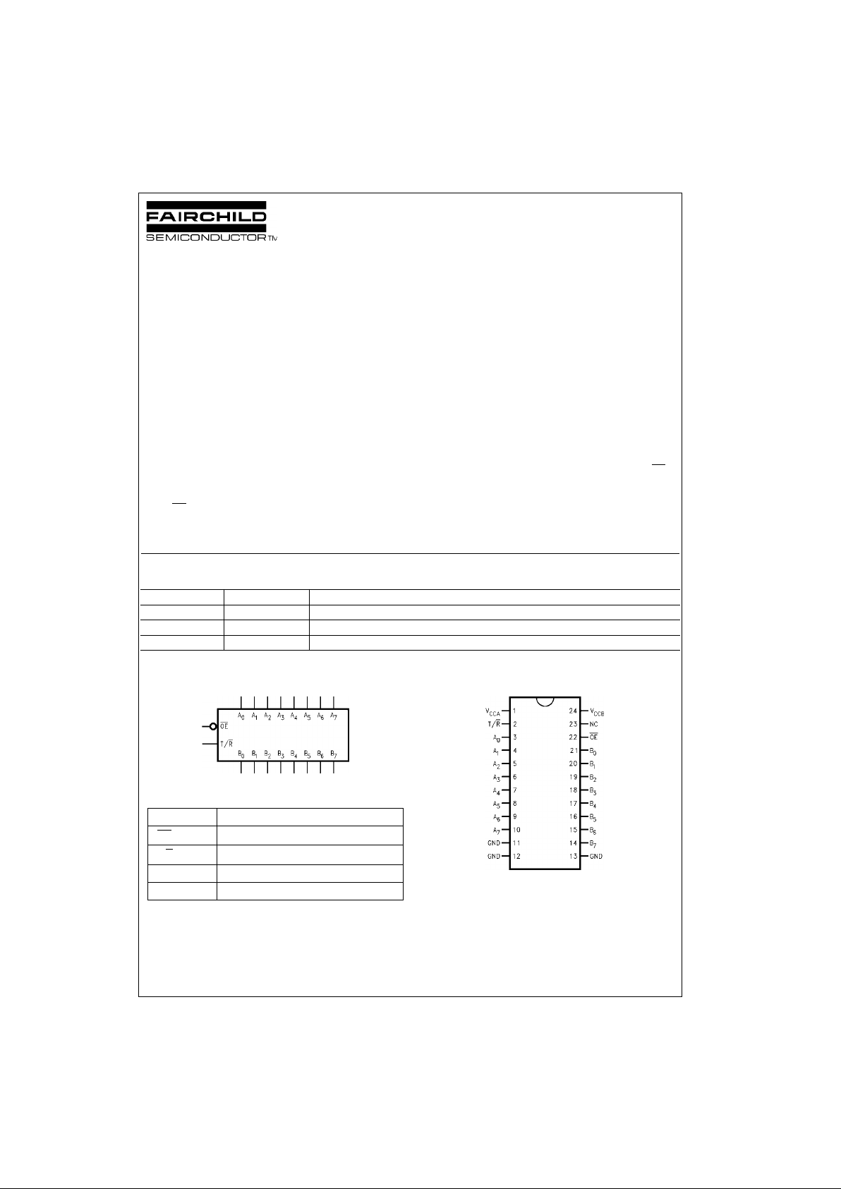
Logic Symbol
Pin Descriptions
Connection Diagram
Order Number Package Number Package Description
74LVXC3245WM M24B 24-Lead Small Outline Integrated Circuit (SOIC), JEDEC MS-013, 0.300” Wide
74LVXC3245QSC MQA24 24-Lead Quarter Size Outline Package (QSOP), JEDEC MO-137, 0.150” Wide
74LVXC3245MTC MTC24 24-Lead Thin Shrink Small Outline Package (TSSOP), JEDEC MO-153, 4.4mm Wide
Pin Names Description
OE
Output Enable Input
T/R
Transmit/Receive Input
A
0–A7
Side A Inputs or 3-STATE Outputs
B
0–B7
Side B Inputs or 3-STATE Outputs
Page 2
www.fairchildsemi.com 2
74LVXC3245
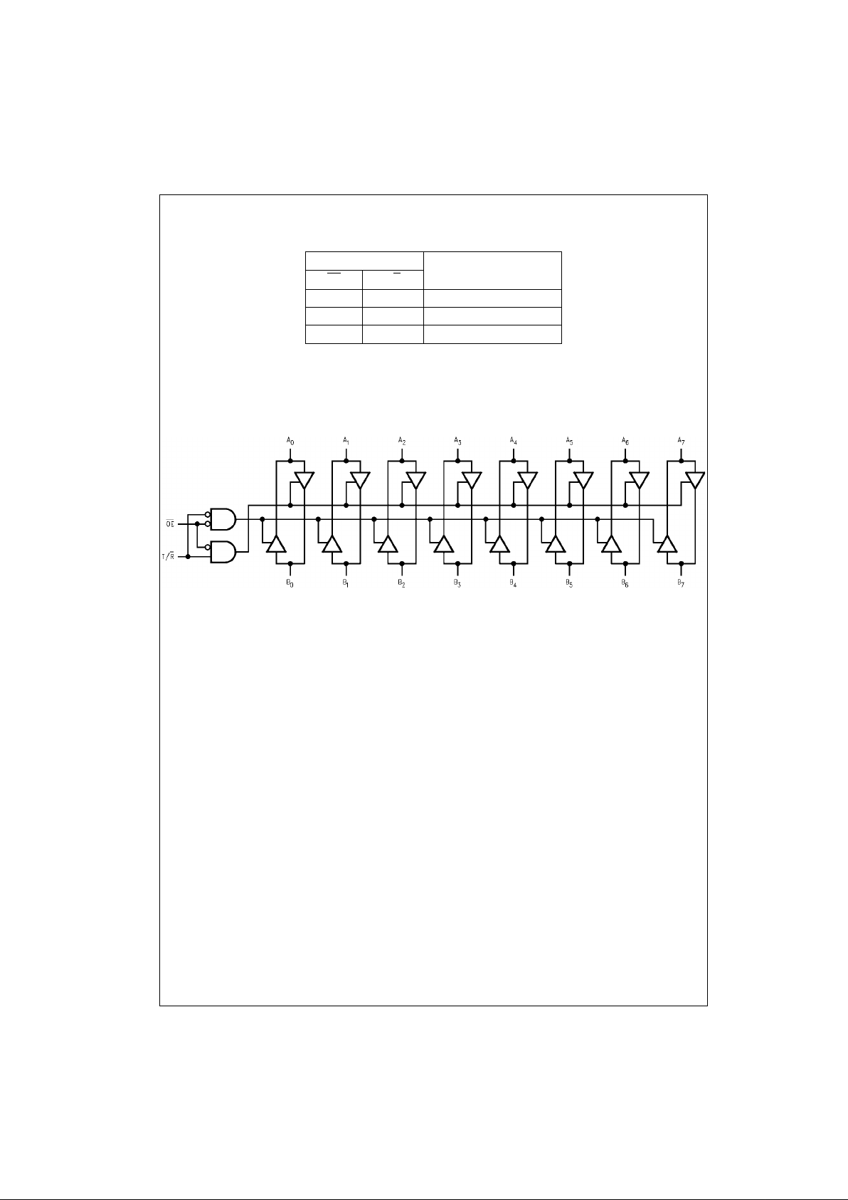
Truth Table
H = HIGH Voltage Level
L = LOW Voltage Level
X = Immaterial
Logic Diagram
Inputs Outputs
OE
T/R
L L Bus B Data to Bus A
L H Bus A Data to Bus B
H X HIGH-Z State
Page 3
3 www.fairchildsemi.com
74LVXC3245
Absolute Maximum Ratings(Note 1) Recommended Operating
Conditions
(Note 2)
Note 1: The “Absolute Maximum Ratings ” are those val ues beyond w hich
the safety of the device cannot be guaranteed. The device should not be
operated at these limits. The parametric values defined in the Electrical
Characteristics tables are not guaranteed at the absolute maximum ratings.
The “Recommend ed O peratin g Cond itions” t able w ill defin e the condition s
for actual device operation.
Note 2: The A Port unused pins (inputs or I/Os) must be held HIGH or
LOW. They may not float.
DC Electrical Characteristics
Supply Voltage (V
CCA
, V
CCB
) −0.5V to +7.0V
DC Input Voltage (V
I
) @ OE, T/R −0.5V to V
CCA
+0.5V
DC Input/Output Voltage (V
I/O
)
@ A
n
−0.5V to V
CCA
+0.5V
@ B
n
−0.5V to V
CCB
+0.5V
DC Input Diode Current (I
IK
)
@ OE
, T/R ±20 mA
DC Output Diode (I
OK
) Current ±50 mA
DC Output Source or Sink Current (I
O
) ±50 mA
DC V
CC
or Ground Current
per Output Pin (I
CC
or I
GND
) ±50 mA
and Max Current ±200 mA
Storage Temperature Range (T
STG
) −65°C to +150°C
DC Latch-Up Source or Sink Current ±300 mA
Supply Voltage
V
CCA
2.7V to 3.6V
V
CCB
3.0V to 5.5V
Input Voltage (V
I
) @ OE, T/R 0V to V
CCA
Input Output Voltage (V
I/O
)
@ A
n
0V to V
CCA
@ B
n
0V to V
CCB
Free Air Operating Temperature (TA) −40°C to +85°C
Minimum Input Edge Rate (∆V/∆t) 8 ns/V
V
IN
from 30% to 70% of V
CC
VCC @ 3.0V, 4.5V, 5.5V
Symbol Parameter
V
CCA
(V)
V
CCB
(V)
TA = 25°CTA = −40°C to +85°C
Units Conditions
Typ Guaranteed Limits
V
IHA
Minimum HIGH An, 2.7 3.0 2.0 2.0
V
V
OUT
≤ 0.1V
or
≥VCC − 0.1V
Level Input
OE
3.0 3.6 2.0 2.0
Voltage
T/R
3.6 5.5 2.0 2.0
V
IHB
B
n
2.7 3.0 2.0 2.0
3.0 3.6 2.0 2.0
3.6 5.5 3.85 3.85
V
ILA
Maximum LOW An, 2.7 3.0 0.8 0.8
V
V
OUT
≤ 0.1V
or
≥VCC − 0.1V
Level Input
OE
3.0 3.6 0.8 0.8
Voltage
T/R
3.6 5.5 0.8 0.8
V
ILB
B
n
2.7 3.0 0.8 0.8
3.0 3.6 0.8 0.8
3.6 5.5 1.65 1.65
V
OHA
Minimum HIGH Level 3.0 3.0 2.99 2.9 2.9
V
I
OUT
= −100 µA
Output Voltage 3.0 3.0 2.85 2.56 2.46 IOH = −12 mA
3.0 3.0 2.65 2.35 2.25 IOH = −24 mA
2.7 3.0 2.5 2.3 2.2 IOH = −12 mA
2.7 4.5 2.3 2.1 2.0 IOH = −24 mA
V
OHB
3.0 3.0 2.99 2.9 2.9
V
I
OUT
= −100 µA
3.0 3.0 2.85 2.56 2.46 IOH = −12 mA
3.0 3.0 2.65 2.35 2.25 IOH = −24 mA
3.0 4.5 4.25 3.86 3.76 IOH = −24 mA
V
OLA
Maximum LOW Level 3.0 3.0 0.002 0.1 0.1
V
I
OUT
= 100 µA
Output Voltage 3.0 3.0 0.21 0.36 0.44 IOL = 24 mA
2.7 3.0 0.11 0.36 0.44 IOL = 12 mA
2.7 4.5 0.22 0.42 0.5 IOL = 24 mA
V
OLB
3.0 3.0 0.002 0.1 0.1
V
I
OUT
= 100 µA
3.0 3.0 0.21 0.36 0.44 IOL = 24 mA
3.0 4.5 0.18 0.36 0.44 IOL = 24 mA
I
IN
Maximum Input 3.6 3.6 ±0.1 ±1.0
µA
VI = V
CCA
, GND
Leakage Current @ 3.6 5.5 ±0.1 ±1.0
OE, T/R
Page 4

www.fairchildsemi.com 4
74LVXC3245
DC Electrical Characteristics (Continued)
Note 3: Worst case package.
Note 4: Max number of outputs defined a s (n ). D at a inputs are driven 0V to V
CC
level; one output at GND.
Note 5: Max number of Data Inputs (n) swit c hing. (n–1) inputs switc hing 0V to V
CC
level. Input-under-test switching:
V
CC
level to threshold (V
IHD
), 0V to threshold (V
ILD
), f = 1 MHz.
Symbol Parameter
V
CCA
(V)
V
CCB
(V)
TA = 25°CTA = −40°C to +85°C
Units Conditions
Typ Guaranteed Limits
I
OZA
Maximum 3-STATE 3.6 3.6 ±0.5 ±5.0
µA
VI = VIL, VIH,
Output Leakage
3.6 5.5 ±0.5 ±5.0
OE = V
CCA
@ A
n
VO = V
CCA
, GND
I
OZB
Maximum 3-STATE 3.6 3.6 ±0.5 ±5.0
µA
VI = VIL, VIH,
Output Leakage
3.6 5.5 ±0.5 ±5.0
OE = V
CCA
@ B
n
VO = V
CCB
, GND
∆I
CC
Maximum B
n
3.6 5.5 1.0 1.35 1.5
mA
VI = V
CCB
–2.1V
ICC/Input All Inputs 3.6 3.6 0.35 0.5 VI = VCC–0.6V
I
CCA1
Quiescent V
CCA
An = V
CCA
or GND
Supply Current 3.6 Open 5 50
µA
Bn = Open, OE = V
CCA
,
as B Port Floats
T/R = V
CCA
, V
CCB
= Open
I
CCA2
Quiescent V
CCA
3.6 3.6 5 50
µA
An = V
CCA
or GND,
Supply Current 3.6 5.5 5 50 Bn = V
CCB
or GND,
OE = GND, T/R = GND
I
CCB
Quiescent V
CCB
3.6 3.6 5 50
µA
An = V
CCA
or GND,
Supply Current 3.6 5.5 8 80 Bn = V
CCB
or GND,
OE = GND, T/R = V
CCA
V
OLPA
Quiet Output 3.3 3.3 0.8
V
(Note 3)(Note 4)
Maximum Dynamic 3.3 5.0 0.8
V
OLPBVOL
3.3 3.3 0.8
V
(Note 3)(Note 4)
3.3 5.0 1.5
V
OLVA
Quiet Output 3.3 3.3 −0.8
V
(Note 3)(Note 4)
Minimum Dynamic 3.3 5.0 −0.8
V
OLVBVOL
3.3 3.3 −0.8
V
(Note 3)(Note 4)
3.3 5.0 −1.2
V
IHDA
Minimum HIGH 3.3 3.3 2.0
V
(Note 3)(Note 5)
Level Dynamic 3.3 5.0 2.0
V
IHDB
Input Voltage 3.3 3.3 2.0
V
(Note 3)(Note 5)
3.3 5.0 3.5
V
ILDA
Maximum LOW 3.3 3.3 0.8
V
(Note 3)(Note 5)
Level Dynamic 3.3 5.0 0.8
V
ILDB
Input Voltage 3.3 3.3 0.8
V
(Note 3)(Note 5)
3.3 5.0 1.5
Page 5

5 www.fairchildsemi.com
74LVXC3245
AC Electrical Characteristics
Note 6: Typical values at V
CCA
= 3.3V, V
CCB
= 5.0V @ 25°C.
Note 7: Typical values at V
CCA
= 3.3V, V
CCB
= 3.3V @ 25°C.
Note 8: Skew is def ined as the absol ut e v alue of the difference between the actu al propagation del ay f or any two separate outputs of the same device. The
specification applies to any out puts switching in the same direction, either HIGH-to-LOW (t
OSHL
) or LOW-to-HIGH (t
OSLH
). Parameter guaranteed by design.
Capacitance
Note 9: CPD is measured at 10 MHz.
Symbol Parameter
TA = +25°CT
A
= −40°C to +85°CT
A
= +25°CT
A
= −40°C to +85°C
Units
CL = 50 pF CL = 50 pF CL = 50 pF CL = 50 pF
V
CCA
= 2.7V–3.6V V
CCA
= 2.7V–3.6V V
CCA
= 2.7V–3.6V V
CCA
= 2.7V–3.6V
V
CCB
= 4.5V–5.5V V
CCB
= 4.5V–5.5V V
CCB
= 3.0V–3.6V V
CCB
= 3.0V–3.6V
Min Typ Max Min Max Min Typ Max Min Max
(Note 6) (Note 7)
t
PHL
Propagation Delay 1.0 4.8 8.0 1.0 8.5 1.0 5.5 8.5 1.0 9.0
ns
t
PLH
A to B 1.0 3.9 6.5 1.0 7.0 1.0 5.2 8.0 1.0 8.5
t
PHL
Propagation Delay 1.0 3.8 6.5 1.0 7.0 1.0 4.4 7.0 1.0 7.5
ns
t
PLH
B to A 1.0 4.3 7.5 1.0 8.0 1.0 5.1 7.5 1.0 8.0
t
PZL
Output Enable Time 1.0 4.7 8.0 1.0 8.5 1.0 6.0 9.0 1.0 9.5
ns
t
PZH
OE to B
1.0 4.8 8.5 1.0 9.0 1.0 6.1 9.5 1.0 10.0
t
PZL
Output Enable Time 1.0 5.9 9.5 1.0 10.0 1.0 6.4 10.0 1.0 10.5
ns
t
PZH
OE to A
1.0 5.4 9.0 1.0 9.5 1.0 5.8 9.0 1.0 9.5
t
PHZ
Output Disable Time 1.0 4.0 8.0 1.0 8.5 1.0 6.3 9.5 1.0 10.0
ns
t
PLZ
OE to B
1.0 3.8 7.5 1.0 8.0 1.0 4.5 8.0 1.0 8.5
t
PHZ
Output Disable Time 1.0 4.6 9.5 1.0 10.0 1.0 5.2 9.5 1.0 10.0
ns
t
PLZ
OE to A
1.0 3.1 6.5 1.0 7.0 1.0 3.4 6.5 1.0 7.0
t
OSHL
Output to Output
t
OSLH
Skew (Note 8) 1.0 1.5 1.5 1.0 1.5 1.5 ns
Data to Output
Symbol Parameter Typ Units Conditions
C
IN
Input Capacitance 4.5 pF VCC = Open
C
I/O
Input/Output Capacitance 10 pF V
CCA
= 3.3V
V
CCB
= 5.0V
C
PD
Power Dissipation A→B50pFV
CCB
= 5.0V
Capacitance (Note 9) B→A40pFV
CCA
= 3.3V
Page 6

www.fairchildsemi.com 6
74LVXC3245
Power Up Considerations
To insure the system does not experience unnecessary I
CC
current draw, bus contention, o r oscillations during pow er
up, the following gu idelines should be adhered to (re fer to
Table 1):
• Power up the control side of the device first. Th is is the
V
CCA
side.
•OE
should ramp with or ahead of V
CCA
. This will help
guard against bus contention.
• The Transmit/Receive control pin (T/R
) should ramp with
V
CCA
, this will ensure that the A Port data pins are con -
figured as inputs. With V
CCA
receiving power fir st, the A
I/O Port should be configured as inp uts to help guard
against bus contention and oscillations.
• A side data inputs should be driven to a vali d log ic l evel.
This will prevent excessive current draw.
The above steps will ensure that no bus contention or oscillations, and therefore no excessive current draw occurs
during the power up cycling of the se devices. These steps
will help prevent possible damage to the tran slato r devices
and potential damage to other system components.
TABLE 1. Low Voltage Translator Power Up Sequencing Table
Please reference Application Note AN-5001 for more detailed information on using Fairchild’s LVX Low Voltage Dual
Supply CMOS Translating Transceivers.
Configurable I/O Application for PCMCIA Cards
Block Diagram
The LVXC3245 is a 24-pin dual su pply device well sui ted
for PCMCIA configurable I/O applications. Ideal for low
power notebook designs, the LVXC3245 consumes less
than 1 mW of quiescent power in all modes o f operation.
The LVXC3245 meets all PCMCIA I/O voltage requirements at 5V and 3.3V operation. By tying V
CCB
of the
LVXC3245 to the card voltage supply, the PCMCIA card
will always experience rail to rail output swings, maximizing
the reliability of the interface.
The V
CCA
pin on the LVXC3245 must always be tied to a
3V power supply. This voltage connection provide s inter na l
references needed to account for variations in V
CCB
. When
connected as in the f igure a bove, the LVXC3245 meets all
the voltage and cur rent require ments of the IS A bus standard (IEEE P996).
Device Type
V
CCA
V
CCB
T/R OE A Side I/O B Side I/O
Floatable Pin
Allowed
74LVXC3245
3V 3V to 5.5V ramp ramp logic
outputs
yes, V
CCB
and B
(power up 1st) configurable with V
CCA
with V
CCA
0V or V
CCA
I/O’s w/ OE HIGH
Page 7

7 www.fairchildsemi.com
74LVXC3245
Physical Dimensions inches (millimeters) unless otherwise noted
24-Lead Small Outline Integrated Circuit (SOIC), JEDEC MS-013, 0.300” Wide
Package Number M24B
24-Lead Quarter Size Outline Package (QSOP), JEDEC MO-37, 0.150” Wide
Package Number MQA24
Page 8

www.fairchildsemi.com 8
74LVXC3245 8-Bit Dual Supply Configurable Voltage Interface Transceiver with 3-STATE Outputs
Physical Dimensions inches (millimeters) unless otherwise noted (Continued)
24-Lead Thin Shrink Small Outline Package (TSSOP), JEDEC MO-153, 4.4mm Wide
Package Number MTC24
Fairchild does not assume any responsibility for use of any circuitry described, no circuit pate nt licenses are implied and
Fairchild reserves the right at any time without notice to change said circuitry and specifications.
LIFE SUPPORT POLICY
FAIRCHILD’S PRODUCTS ARE NOT AUTHORIZED FOR USE AS CRITICAL COMPONENTS IN LIFE SUPPORT
DEVICES OR SYSTEMS WITHOUT THE EXPRESS WRITTEN APPROVAL OF THE PRESIDENT OF FAIRCHILD
SEMICONDUCTOR CORPORATION. As used herein:
1. Life support devices or systems are devices or syste ms
which, (a) are intended for surgical implant into the
body, or (b) support or sustain life, and (c) whose failure
to perform when properly used in accordance with
instructions for use provided in the labeling, can be reasonably expected to result in a significant inju ry to the
user.
2. A critical component i n any compon ent of a lif e support
device or system whose failu re to perform can be reasonably expected to ca use the fa i lure of the life su pp ort
device or system, or to affect its safety or effectiveness.
www.fairchildsemi.com
 Loading...