

Page 1
74LVX86
LOW VOLTAGE CMOS QUAD EXCLUSIVE OR GATE
WITH 5V TOLERANT INPUTS
■ HIGH SPEED:
t
= 5.8 ns (TYP.) at V
PD
■ 5V TOLERANT INPUTS
■ INPUT VOLTAG E LEVEL:
V
=0.8V , VIH=2V at VCC=3V
IL
■ LOW POWER DISSIPATION:
I
= 2 µA (MAX.) at TA=25°C
CC
■ LOW NOISE:
V
= 0.3V (TYP.) at VCC = 3.3V
OLP
■ SYMMETRICAL OUTPUT IMPEDANCE:
|I
| = IOL = 4mA (MIN)
OH
■ BALANCED PROPAGATION DELAYS:
t
≅ t
PLH
PHL
■ OPERATING VOLTAGE RANGE:
V
(OPR) = 2V to 3.6V (1.2V Data Retention)
CC
■ PIN AND FUNCTION COMPATIBLE WITH
CC
= 3.3V
74 SERIES 86
■ IMPROVED LATCH-UP IMMUNITY
■ POWER DOWN PROTECTION ON INPUTS
DESCRIPTION
The 74LVX86 is a low voltage CMOS QUAD
EXCLUSIVE OR GATE fabricated with
sub-micron silicon gate and double-layer metal
wiring C
2
MOS technology. It is ideal for low
TSSOPSOP
Table 1: Order Codes
PACKAGE T & R
SOP 74LVX86MTR
TSSOP 74LVX86TTR
power, battery operated and low noise 3.3V
applications.
Power down protection is provided on all inputs
and 0 to 7V can be accepted on inputs with no
regard to the supply voltage.
This device can be used to interface 5V to 3V
system. It combines high speed performance with
the true CMOS low power consumption. All inputs
and outputs are eq uipped with protection circuits
against static discharge, giving them 2KV ESD
immunity and transient excess voltage.
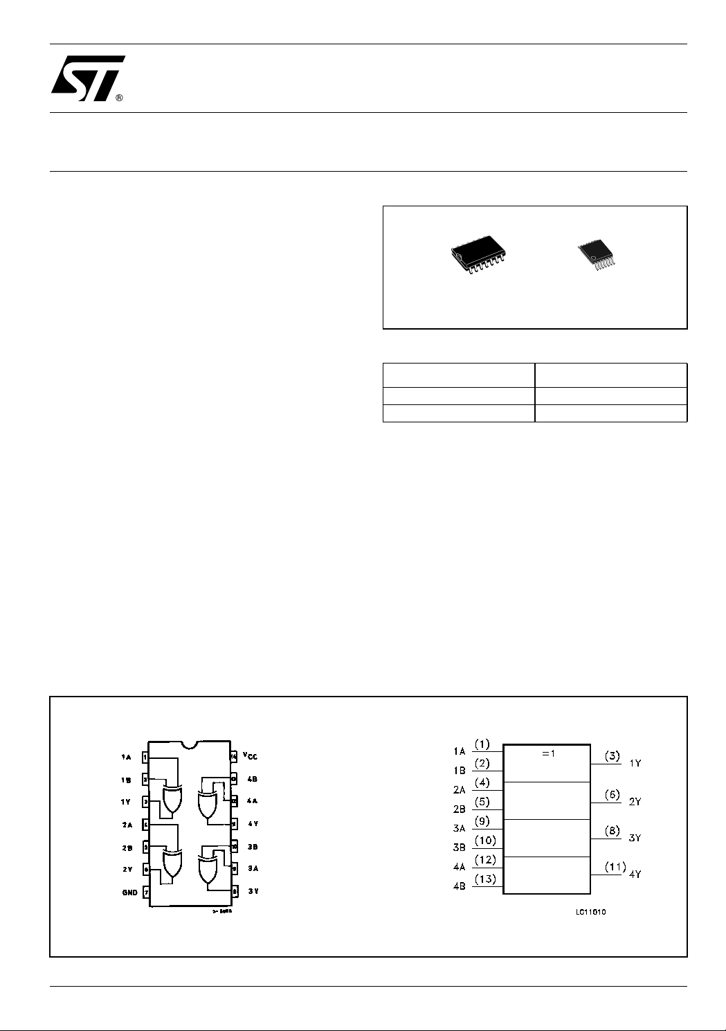
Figure 1: Pin Connection And IEC Logic Symbols
Rev. 4
1/11August 2004
Page 2
74LVX86
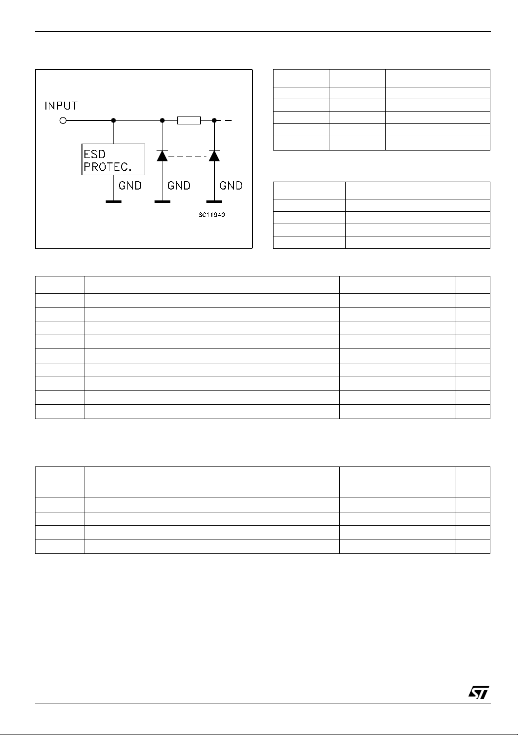
Figure 2: Input Equivalent Circuit Table 2: Pin Description
PIN No SYMBOL NAME AND FUNCTION
1, 4, 9, 12 1A to 4A Data Inputs
2, 5, 10, 13 1B to 4B Data Inputs
3, 6, 8, 11 1Y to 4Y Data Outputs
7 GND Ground (0V)
14
Table 3: Truth Table
ABY
LLL
LHH
HLH
HHL
Table 4: Absolute Maximum Ratings
Symbol Parameter Value Unit
V
V
V
I
I
OK
I
or I
I
CC
T
T
Absolute Maximum Ratings are those values beyond which damage to the device may occur. Functional operation under these conditions is
not implied.
Supply Voltage
CC
DC Input Voltage
I
DC Output Voltage -0.5 to VCC + 0.5
O
DC Input Diode Current
IK
DC Output Diode Current
DC Output Current
O
DC VCC or Ground Current
GND
Storage Temperature
stg
Lead Temperature (10 sec)
L
Table 5: Recommended Operating Conditions
V
CC
Positive Supply Voltage
-0.5 to +7.0 V
-0.5 to +7.0 V
- 20 mA
± 20 mA
± 25 mA
± 50 mA
-65 to +150 °C
300 °C
V
Symbol Parameter Value Unit
V
V
V
T
dt/dv
1) Truth T abl e guarante ed: 1.2V to 3.6V
2) VIN from 0.8V to 2.0V
Supply Voltage (note 1)
CC
Input Voltage
I
Output Voltage 0 to V
O
Operating Temperature
op
Input Rise and Fall Time (note 2) (V
= 3.3V)
CC
2 to 3.6 V
0 to 5.5 V
CC
-55 to 125 °C
0 to 100 ns/V
2/11
V
Page 3
Table 6: DC Specifications
Symbol Parameter
V
V
V
High Level Input
IH
Voltage
V
Low Level Input
IL
Voltage
High Level Output
OH
Voltage
Low Level Output
OL
Voltage
Input Leakage
I
I
Current
I
Quiescent Supply
CC
Current
Test Condition Value
V
(V)
CC
T
A
Min. Typ. Max. Min. Max. Min. Max.
-40 to 85°C -55 to 125°C
= 25°C
2.0 1.5 1.5 1.5
3.6 2.4 2.4 2.4
2.0 0.5 0.5 0.5
3.6 0.8 0.8 0.8
=-50 µA
2.0
3.0
2.0
3.0
3.6
3.6
I
O
=-50 µA
I
O
=-4 mA
I
O
IO=50 µA
I
=50 µA
O
=4 mA
I
O
= 5V or GND
V
I
V
= VCC or GND
I
1.9 2.0 1.9 1.9
2.9 3.0 2.9 2.9
2.58 2.48 2.4
0.0 0.1 0.1 0.1
0.0 0.1 0.1 0.1
0.36 0.44 0.55
± 0.1 ± 1 ± 1 µA
22020µA
74LVX86
Unit
V3.0 2.0 2.0 2.0
V3.0 0.8 0.8 0.8
V3.0
V3.0
Table 7: Dynamic Switching Characteristics
Test Condition Value
= 25°C
Symbol Parameter
V
V
V
Dynamic Low
OLP
Voltage Quiet
OLV
Output (note 1, 2)
Dynamic High
IHD
Voltage Input (note
V
CC
(V)
3.3
3.3 2
= 50 pF
C
L
T
A
Min. Typ. Max. Min. Max. Min. Max.
0.3 0.5
-0.5 -0.3
1, 3)
V
Dynamic Low
ILD
Voltage Input (note
3.3 0.8
1, 3)
1) Worst case package.
2) Max number of outp ut s defined as (n). Data inp ut s are driven 0V to 3.3V, (n-1) outputs switc hi ng and one out put at GND.
3) Max number of data inputs (n) switching. (n-1) switching 0V to 3.3V. Inputs under test switching: 3.3V to threshold (V
(V
), f=1MHz.
IHD
-40 to 85°C -55 to 125°C
ILD
Unit
V
), 0V to thresho l d
3/11
Page 4
74LVX86
Table 8: AC Electrical Characteristics (Input tr = tf = 3ns)
Test Condition Value
= 25°C
Symbol Parameter
t
PLH tPHL
t
OSLH
t
OSHL
1) Skew is defined as the absolute value of the difference between the actual propagation delay for any two outputs of the same device switching in the sa m e di rection, ei ther HIGH or LOW
2) Param eter guaran teed by design
(*) Voltage range is 3.3V ±
Propagation Delay
Time
Output To Output
Skew Time (note1,
2)
0.3V
V
C
CC
(V)
L
(pF)
2.7 15 7.5 14.5 1.0 17.5 1.0 17.5
2.7 50 10.0 18.0 1.0 21.0 1.0 21.0
(*)
3.3
3.3
15 5.8 9.3 1.0 11.0 1.0 11.0
(*)
50 8.3 12.8 1.0 14.5 1.0 14.5
2.7 50 0.5 1.0 1.5 1.5
(*)
3.3
50
T
A
Min. Typ. Max. Min. Max. Min. Max.
0.5 1.0 1.5 1.5
Table 9: Capacitive Characteristics
Test Condition Value
= 25°C
Symbol Parameter
C
C
Input Capacitance
IN
Power Dissipation
PD
Capacitance
(note 1)
V
CC
(V)
3.3 4 10 10 10 pF
3.3 18 pF
T
A
Min. Typ. Max. Min. Max. Min. Max.
-40 to 85°C -55 to 125°C
-40 to 85°C -55 to 125°C
Unit
ns
ns
Unit
1) CPD is defined as the value of the IC’s internal equivalent capacitance which is calculated from the operating current consumption without
load. (Refer to Test Circuit). Average operating current can be obtained by the following equation. I
= CPD x VCC x fIN + ICC/4 (per gate)
CC(opr)
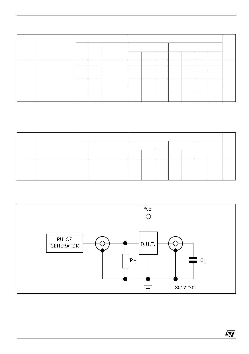
Figure 3: Test Circuit
CL =15/50pF or equivalent (i ncludes jig an d probe capac i tance)
R
= Z
of pulse generator (typically 50Ω)
T
OUT
4/11
Page 5

Figure 4: Waveform - Propagation Delays (f=1MHz; 50% duty cycle)
74LVX86
5/11
Page 6

74LVX86
SO-14 MECHANICAL DATA
DIM.
A 1.35 1.75 0.053 0.069
A1 0.1 0.25 0.004 0.010
A2 1.10 1.65 0.043 0.065
B 0.33 0.51 0.013 0.020
C 0.19 0.25 0.007 0.010
D 8.55 8.75 0.337 0.344
E 3.8 4.0 0.150 0.157
e 1.27 0.050
H 5.8 6.2 0.228 0.244
h 0.25 0.50 0.010 0.020
L 0.4 1.27 0.016 0.050
k0° 8° 0° 8°
ddd 0.100 0.004
MIN. TYP MAX. MIN. TYP. MAX.
mm. inch
6/11
0016019D
Page 7

74LVX86
TSSOP14 MECHANICAL DATA
mm. inch
DIM.
MIN. TYP MAX. MIN. TYP. MAX.
A 1.2 0.047
A1 0.05 0.15 0.002 0.004 0.006
A2 0.8 1 1.05 0.031 0.039 0.041
b 0.19 0.30 0.007 0.012
c 0.09 0.20 0.004 0.0089
D 4.9 5 5.1 0.193 0.197 0.201
E 6.2 6.4 6.6 0.244 0.252 0.260
E1 4.3 4.4 4.48 0.169 0.173 0.176
e 0.65 BSC 0.0256 BSC
K0˚ 8˚0˚ 8˚
L 0.45 0.60 0.75 0.018 0.024 0.030
A2
A
A1
b
e
c
K
L
E
D
E1
PIN 1 IDENTIFICATION
1
0080337D
7/11
Page 8

74LVX86
Tape & Reel SO-14 MECHANICAL DATA
mm. inch
DIM.
MIN. TYP MAX. MIN. TYP. MAX.
A 330 12.992
C 12.8 13.2 0.504 0.519
D 20.2 0.795
N 60 2.362
T 22.4 0.882
Ao 6.4 6.6 0.252 0.260
Bo 9 9.2 0.354 0.362
Ko 2.1 2.3 0.082 0.090
Po 3.9 4.1 0.153 0.161
P 7.9 8.1 0.311 0.319
8/11
Page 9

74LVX86
Tape & Reel TSSOP14 MECHANICAL DATA
mm. inch
DIM.
MIN. TYP MAX. MIN. TYP. MAX.
A 330 12.992
C 12.8 13.2 0.504 0.519
D 20.2 0.795
N 60 2.362
T 22.4 0.882
Ao 6.7 6.9 0.264 0.272
Bo 5.3 5.5 0.209 0.217
Ko 1.6 1.8 0.063 0.071
Po 3.9 4.1 0.153 0.161
P 7.9 8.1 0.311 0.319
9/11
Page 10

74LVX86
Table 10: Revision History
Date Revisio n Description of Changes
27-Aug-2004 4 Ordering Codes Revision - pag. 1.
10/11
Page 11

74LVX86
Information fur nished is believed to be accurate and reliable. However, STMicroelectronics assumes no responsibility for the consequences
of use of s uch inf ormati on nor for a ny infr ing eme nt o f p atent s or o ther ri ghts of third parties wh ich m ay res ult fr om it s us e. No li cens e i s gr an ted
by implication or otherwise under any patent or patent rights of STMicroelectronics. Speci fications mentioned in this publication are subjec t
to change wi thout notice. This publication supersedes and replaces all information previously supplied. STMicroelectronics produc ts are not
authorized for use as critical components in life support devices or systems without express written approval of STMicroelectronics.
The ST logo is a registered trademark of STMicroelectronics
All other names are the property of their respective owners
© 2004 STMicroelectronics - All Rights Reserved
STMicroelectronics group of companies
Australia - Belgium - Brazil - Canada - China - Czech Republic - Finland - France - Germany - Hong Kong - India - Israel - Italy - Japan -
Malaysia - Malta - Morocco - Singapore - Spain - Sweden - Switzerland - United Kingdom - United States of America
www.st.com
11/11
 Loading...