

Page 1
1/10July 2001
■ HIGH SPEED:
f
MAX
= 125MHz (TYP.) at VCC = 3.3V
■ 5V TOLERANT INPUTS
■ POWER-DOWN PROTECTION ON INPUTS
■ INPUT VOLTAGE LEVEL:
V
IL
= 0.8V, VIH = 2V at VCC =3V
■ LOW POWER DISSIPATION:
I
CC
= 4 µA (MAX.) at TA=25°C
■ LOW NOISE:
V
OLP
= 0.3V (TYP.) at VCC =3.3V
■ SYMMETRICAL OUTPUT IMPEDANCE:
|I
OH
| = IOL = 4 mA (MIN) at VCC =3V
■ BALANCED PROPAGATION DELAYS:
t
PLH
≅ t
PHL
■ OPERATING VOLTAGE RANGE:
V
CC
(OPR) = 2V to 3.6V (1.2V Data Retention)
■ PIN AND FUNCTION COMPATIBLE WITH
74 SERIES 574
■ IMPROVED LATCH-UP IMMUNITY
DESCRIPTION
The 74LVX574 is a low voltage CMOS OCTAL
D-TYPE FLIP- FLO P with 3 STAT E OUT PUT NON
INVERTING fabricated with sub-micron silicon
gate and double-layer metal wiring C
2
MOS
technology. It is ideal for low power, battery
operated and low noise 3.3V applications.
This 8 bit D-Type flip-flop is controlled by a clock
input (CK) and an out put enable input (OE
). O n
the positive transition of th e clock, the Q outputs
will be set to the logic state that were set up at t he
D inputs. While the (OE
) input is low, the 8 outputs
will be in a norm al logic state (high or low logic
level) and while high le vel the outpu ts will be in a
high impedance state. The output control does not
affect the internal operation of flip flops; that is,
the old data can be retained or the new data can
be entered even while the outputs are off.
Power down protection is provided on all inputs
and 0 to 7V can be accepted on inputs with no
regard to the supply voltage.
This device can be used to interface 5V to 3V. It
combines high speed performance with the true
CMOS low power consumption.
All inputs and outputs are equipped with
protection circuits against stat ic discharge, giving
them 2KV ESD immunity and transient excess
voltage.
74LVX574
LOW VOLTAGE CMOS OCTAL D-TYPE FLIP-FLOP
(3-STATE NON INV.) WITH 5V TOLERANT INP UTS
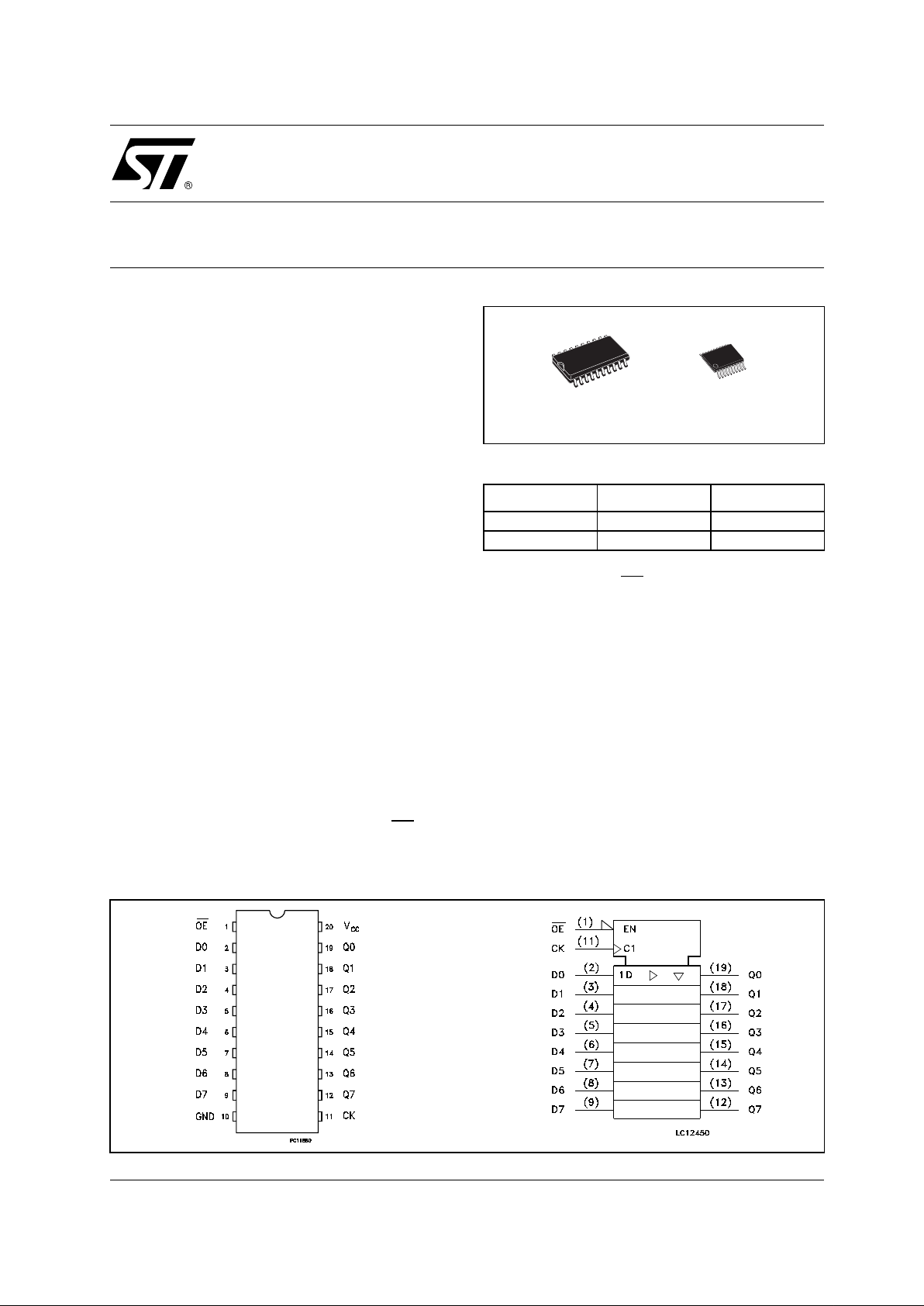
PIN CONNECTION AND IEC LOGIC SYMBOLS
ORDER CODES
PACKAGE TUBE T & R
SOP 74LVX574M 74LVX574MTR
TSSOP 74LVX574TTR
TSSOPSOP
Page 2
74LVX574
2/10
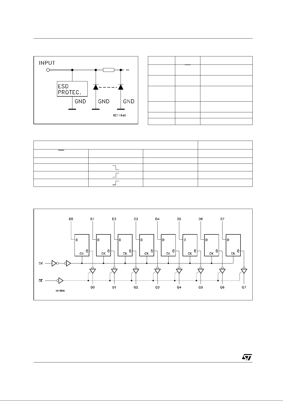
INPUT EQUIVALENT CIRCUIT PIN DESCRIPTION
TRUTH TABLE
X : Don’t Care
Z : High Impedance
LOGIC DIAGRAM
This log i c diagram has not be used to e st i m ate propagation dela ys
PIN No SYMBOL NAME AND FUNCTION
1OE
3-State Output Enable
Input (Active LOW)
2, 3, 4, 5, 6,
7, 8, 9
D0 to D7 Data Inputs
12, 13, 14,
15, 16, 17,
18, 19
Q0 to Q7 3-State Outputs
1 1 CK Clock Input (LOW-to-HIGH
Edge Triggered)
10 GND Ground (0V)
20 V
CC
Positive Supply Voltage
INPUTS OUTPUT
OE
CK D Q
HXXZ
L X NO CHANGE
LLL
LHH
Page 3
74LVX574
3/10
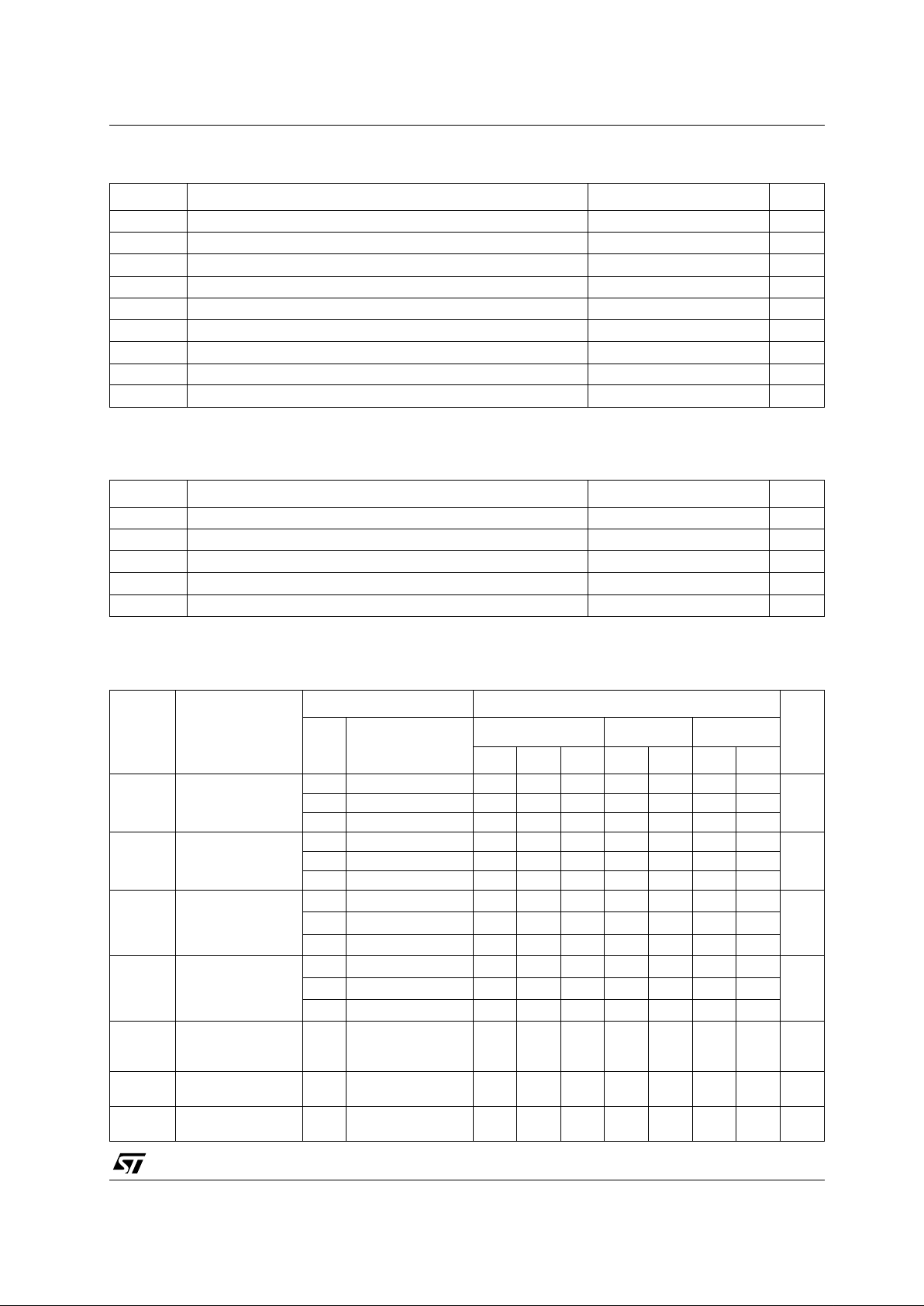
ABSOLUTE MAXIMUM RATINGS
Absolute Maximum Ratings are those values beyond which damage to the device may occur. Functional operation under these conditions is
not implied
RECOMMENDED OPERATING CONDITIONS
1) Truth T abl e guaranteed: 1.2V to 3.6V
2) V
IN
from 0.8V to 2.0V
DC SPECIFICATIONS
Symbol Parameter Value Unit
V
CC
Supply Voltage
-0.5 to +7.0 V
V
I
DC Input Voltage
-0.5 to +7.0 V
V
O
DC Output Voltage -0.5 to VCC + 0.5
V
I
IK
DC Input Diode Current
- 20 mA
I
OK
DC Output Diode Current
± 20 mA
I
O
DC Output Current
± 25 mA
I
CC
or I
GND
DC VCC or Ground Current
± 50 mA
T
stg
Storage Temperature
-65 to +150 °C
T
L
Lead Temperature (10 sec)
300 °C
Symbol Parameter Value Unit
V
CC
Supply Voltage (note 1)
2 to 3.6 V
V
I
Input Voltage
0 to 5.5 V
V
O
Output Voltage 0 to V
CC
V
T
op
Operating Temperature
-55 to 125 °C
dt/dv
Input Rise and Fall Time (note 2) (V
CC
= 3V)
0 to 100 ns/V
Symbol Parameter
Test Condition Value
Unit
V
CC
(V)
T
A
= 25°C
-40 to 85°C -55 to 125°C
Min. Typ. Max. Min. Max. Min. Max.
V
IH
High Level Input
Voltage
2.0 1.5 1.5 1.5
V3.0
2.0 2.0 2.0
3.6
2.4 2.4 2.4
V
IL
Low Level Input
Voltage
2.0 0.5 0.5 0.5
V3.0 0.8 0.8 0.8
3.6 0.8 0.8 0.8
V
OH
High Level Output
Voltage
2.0
IO=-50 µA
1.9 2.0 1.9 1.9
V3.0
I
O
=-50 µA
2.9 3.0 2.9 2.9
3.0
I
O
=-4 mA
2.58 2.48 2.4
V
OL
Low Level Output
Voltage
2.0
IO=50 µA
0.0 0.1 0.1 0.1
V3.0
I
O
=50 µA
0.0 0.1 0.1 0.1
3.0
I
O
=4 mA
0.36 0.44 0.55
I
OZ
High Impedance
Output Leakage
Current
3.6
V
I
= VIH or V
IL
VO = VCC or GND
±0.25 ± 2.5 ± 2.5 µA
I
I
Input Leakage
Current
3.6
V
I
= 5V or GND
± 0.1 ± 1 ± 1 µA
I
CC
Quiescent Supply
Current
3.6
V
I
= VCC or GND
44040µA
Page 4

74LVX574
4/10
DYNAMIC SWITCHING CHARACTERISTICS
1) Worst c ase package.
2) Max number of outp uts defined as (n). Data inputs are dr i ven 0V to 3.3V, (n-1) outputs switching and one output at GND.
3) Max number of data inputs (n) switching. (n-1) switching 0V to 3.3V. Inputs under test switching: 3.3V to threshold (V
ILD
), 0V to threshold
(V
IHD
), f=1MHz.
AC ELECTRICAL CHARACTERISTICS (Input tr = tf = 3ns)
1) Skew is defined as the absolute value of the difference between the actual propagation delay for any two outputs of the same device switching in the same direc tion, either HIGH or LOW
2) Param eter guaranteed by desi gn
(*) Vol tage range is 3.3V ±
0.3V
Symbol Parameter
Test Condition Value
Unit
V
CC
(V)
T
A
= 25°C
-40 to 85°C -55 to 125°C
Min. Typ. Max. Min. Max. Min. Max.
V
OLP
Dynamic Low
Voltage Quiet
Output (note 1, 2)
3.3
C
L
= 50 pF
0.3 0.8
V
V
OLV
-0.8 -0.3
V
IHD
Dynamic High
Voltage Input
(note 1, 3)
3.3 2.0
V
ILD
Dynamic Low
Voltage Input
(note 1, 3)
3.3 0.8
Symbol Parameter
Test Condition Value
Unit
V
CC
(V)
C
L
(pF)
T
A
= 25°C
-40 to 85°C -55 to 125°C
Min. Typ. Max. Min. Max. Min. Max.
t
PLH
t
PHL
Propagation Delay
Time
CK to Q
2.7
15 9.2 14.5 1.0 17.5 1.0 17.5
ns
2.7
50 11.5 18.0 1.0 21.0 1.0 21.0
3.3
(*)
15 8.5 13.2 1.0 15.5 1.0 15.5
3.3
(*)
50 11.0 16.7 1.0 19.0 1.0 19.0
t
PZL
t
PZH
Output Enable
Time
2.7 15 9.8 15.0 1.0 18.5 1.0 18.5
ns
2.7 50 11.4 18.5 1.0 22.0 1.0 22.0
3.3
(*)
15 8.2 12.8 1.0 15.0 1.0 15.0
3.3
(*)
50 10.7 16.3 1.0 18.5 1.0 18.5
t
PLZ
t
PHZ
Output Disable
Time
2.7 50 12.1 19.1 1.0 22.0 1.0 22.0
ns
3.3
(*)
50 11.0 15.0 1.0 17.0 1.0 17.0
t
W
CK pulse Width,
HIGH
2.7 50 6.5 7.5 7.5
ns
3.3
(*)
50 5.0 5.0 5.0
t
S
Setup Time D to CK
HIGH or LOW
2.7 50 5.0 5.0 5.0
ns
3.3
(*)
50 3.5 3.5 3.5
t
h
Hold Time D to CK
HIGH or LOW
2.7 50 1.5 1.5 1.5
ns
3.3
(*)
50 1.5 1.5 1.5
f
MAX
Maximum Clock
Frequency
2.7 15 60 115 50 48
MHz
2.7 50 45 60 40 40
3.3
(*)
15 80 125 65 60
3.3
(*)
50 50 75 45 40
t
OSLH
t
OSHL
Output to Output
Skew Time (note
1,2)
2.7 50 0.5 1.0 1.5 1.5
ns
3.3
(*)
50 0.5 1.0 1.5 1.5
Page 5

74LVX574
5/10
CAPACITIVE CHARACTERISTICS
1) CPD is defined as the value of the IC’s internal equivalent capacitance which is calculated from the operating current consumption without
load. (Refer to Test Circuit). Average operating current can be obtained by the following equation. I
CC(opr)
= CPD x VCC x fIN + ICC/8 (per c ircuit )
TEST CIRCUIT
CL =15/50pF or equivalent (i ncludes jig and probe capacitanc e)
R
L
= R1 = 1KΩ or equivalent
R
T
= Z
OUT
of pulse generator (typically 50Ω)
Symbol Parameter
Test Condition Value
Unit
V
CC
(V)
T
A
= 25°C
-40 to 85°C -55 to 125°C
Min. Typ. Max. Min. Max. Min. Max.
C
IN
Input Capacitance
3.3 4101010pF
C
OUT
Output
Capacitance
3.3 6 pF
C
PD
Power Dissipation
Capacitance
(note 1)
3.3
f
IN
= 10MHz
27 pF
TEST SWITCH
t
PLH
, t
PHL
Open
t
PZL
, t
PLZ
V
CC
t
PZH
, t
PHZ
GND
Page 6

74LVX574
6/10
WAVEFORM 1 : PROPAGATION DELAYS SETUP AND HOLD TIMES (f=1M Hz ; 50% duty cycle)
WAVEFORM 2 : OUTPUT ENABLE AND DISABLE TIMES (f=1MH z; 50% duty cycle )
Page 7

74LVX574
7/10
WAVEFORM 3 : CK MINIMUM PULSE WIDTH (f=1MHz; 50% duty cycle)
Page 8

74LVX574
8/10
DIM.
mm. inch
MIN. TYP MAX. MIN. TYP. MAX.
A 2.65 0.104
a1 0.1 0.2 0.004 0.008
a2 2.45 0.096
b 0.35 0.49 0.014 0.019
b1 0.23 0.32 0.009 0.012
C 0.5 0.020
c1 45° (typ.)
D 12.60 13.00 0.496 0.512
E 10.00 10.65 0.393 0.419
e 1.27 0.050
e3 11.43 0.450
F 7.40 7.60 0.291 0.300
L 0.50 1.27 0.020 0.050
M 0.75 0.029
S8° (max.)
SO-20 MECHANICAL DATA
PO13L
Page 9

74LVX574
9/10
DIM.
mm. inch
MIN. TYP MAX. MIN. TYP. MAX.
A 1.2 0.047
A1 0.05 0.15 0.002 0.004 0.006
A2 0.8 1 1.05 0.031 0.039 0.041
b 0.19 0.30 0.007 0.012
c 0.09 0.20 0.004 0.0089
D 6.4 6.5 6.6 0.252 0.256 0.260
E 6.2 6.4 6.6 0.244 0.252 0.260
E1 4.3 4.4 4.48 0.169 0.173 0.176
e 0.65 BSC 0.0256 BSC
K0° 8°0° 8°
L 0.45 0.60 0.75 0.018 0.024 0.030
TSSOP20 MECHANICAL DATA
c
E
b
A2
A
E1
D
1
PIN 1 IDENTIFICATION
A1
L
K
e
0087225C
Page 10

74LVX574
10/10
Information furnished is bel ieved to be accurate and reliable. However, STMicroe lectronics assumes no responsibility for the
consequences of use of such information nor for any infringement of patents or other rights of third parties which may result from
its use. No li cense is granted by i mp lica tion or otherwise under a n y patent or patent rig hts of STMicroelectronics. Spec ific at ions
mentioned in this publication ar e subject to change without notice. This publication supersedes and replaces all information
previously supplied. S TMicroelectronics products are not authorized for use as critica l components in life suppo rt devices or
systems without express written approval of STMicroelectronics.
© The ST logo is a registered trademark of STMicroelectronics
© 2001 STM icroelectronics - Printed in Italy - All Ri g h ts Reserv ed
STMicr o el ectronics G ROU P OF COMPANI E S
Australi a - Brazil - C hi na - Finlan d - F rance - Germ any - Hong Kon g - I ndi a - Italy - Japan - Malaysia - Malta - Morocco
Singapo re - Spain - Sweden - Swi t zerland - United Kingdom
© http://www.st.com
 Loading...