

Datasheet 74LVX574MTCX, 74LVX574MTC, 74LVX574M, 74LVX574SJX, 74LVX574SJ Datasheet (Fairchild Semiconductor)
...Page 1
June 1993
Revised March 1999
74LVX574 Low Voltage Octal D-Type Flip-Flop with 3-STATE Outputs
© 1999 Fairchild Semiconductor Corporation DS500050.prf www.fairchildsemi.com
74LVX574
Low Voltage Octal D-Type Flip-Flop with
3-STATE Outputs
General Description
The LVX574 is a high-speed octal D-type flip-flop which is
controlled by an edge-triggered clock input (CP) and a buffered common Output Enable (OE
) input. When the OE
input is HIGH, the eight outputs are in a high im pedance
state. The LVX574 is functionally identical to the LVX374
but with inputs a nd outpu ts on op posite side s of t he pack-
age. The inputs tolerat e up to 7V allowing interface of 5V
systems to 3V systems.
Features
■ Input voltage translation from 5V to 3V
■ Ideal for low power/low noise 3.3V applications
■ Guaranteed simultaneous switching noise level and
dynamic threshold performance
Ordering Code:
Devices also availab le in Tape and Reel. Specify by appending th e s uffix let t er “X” to the ordering code.
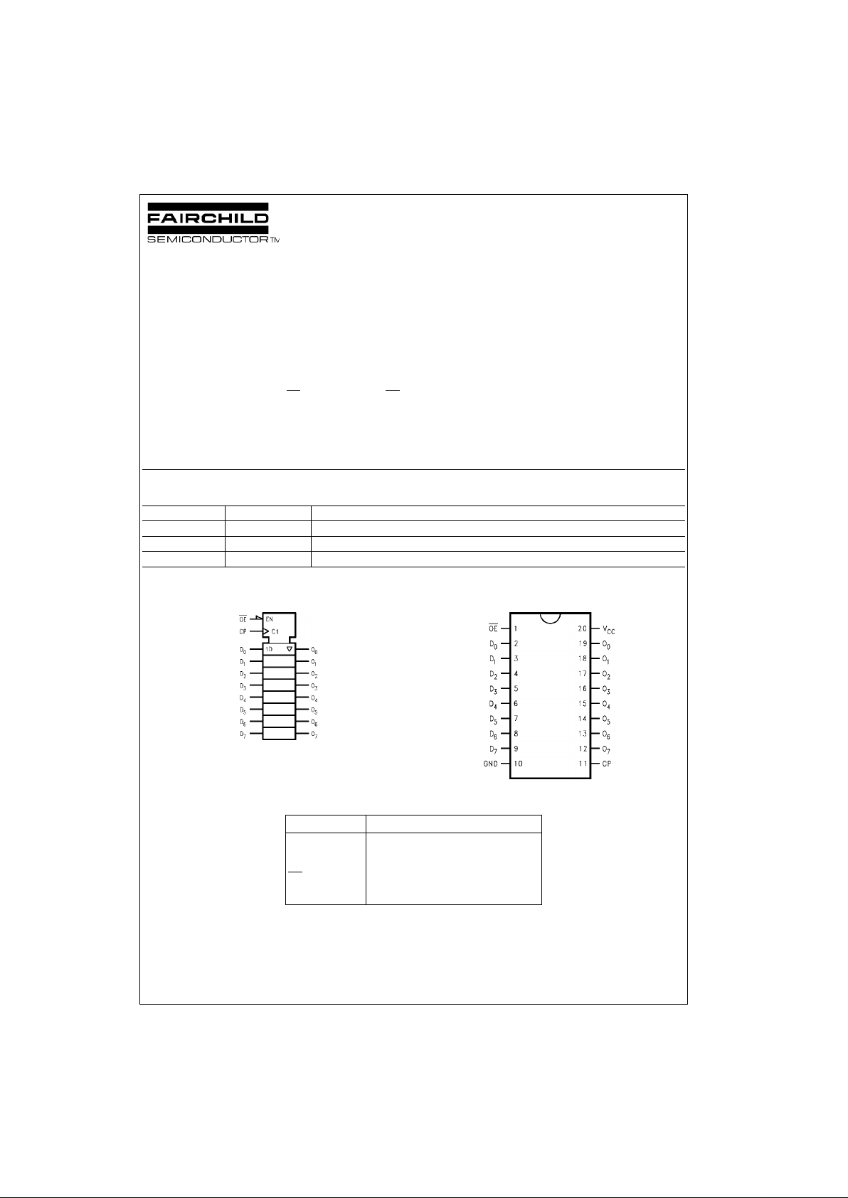
Logic Symbol Connection Diagram
Pin Descriptions
Order Number Package Number Package Description
74LVX574M M20B 20-Lead Small Outline Integrated Circuit (SOIC), JEDEC MS-013, 0.300” Wide
74LVX574SJ M20D 20-Lead Small Outline Package (SOP), EIAJ TYPE II, 5.3mm Wide
74LVX574MTC MTC20 20-Lead Thin Shrink Small Outline Package (TSSOP), JEDEC MO-153, 4.4mm Wide
Pin Names Description
D
0–D7
Data Inputs
CP Clock Pulse Input
OE
3-STATE Output Enable Input
O
0–O7
3-STATE Outputs
Page 2
www.fairchildsemi.com 2
74LVX574
Functional Description
The LVX574 consists of eight e dge-tr iggere d flip -flops with
individual D-type inputs and 3-STATE true outputs. The
buffered clock and buffered Outp ut Enable are com mon to
all flip-flops. The eight flip-flops will store th e state of their
individual D inputs that meet the setup and hold time
requirements on the LOW-to-HIGH Clock (CP) transition.
With the Output Enable (OE
) LOW, the contents of the
eight flip-flops are available at the outputs. When the OE
is
HIGH, the outputs go to th e high impeda nce state. Op eration of the OE
input does not affect t he state of the flip-
flops.
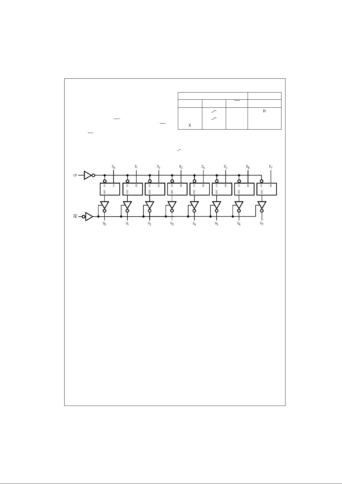
Tr uth Table
H = HIGH Voltage Level
L = LOW Voltage Level
X = Immaterial
Z = High Impedance
= LOW-to-HIGH Transition
Logic Diagram
Please note that this diagram is provided only f or t he understanding of logic operations and should not be used to estimate propagation delays.
Inputs Outputs
D
n
CP OE O
n
H
LH
L
LL
XXH Z
Page 3

3 www.fairchildsemi.com
74LVX574
Absolute Maximum Ratings(Note 1) Recommended Operating
Conditions
(Note 2)
Note 1: The “Absolute Maximum Ratings ” are those val ues beyond w hich
the safety of the device cannot be guaranteed. The device should not be
operated at these limits. The parametric values defined in the Electrical
Characteristics tables are not guaranteed at the absolute maximum ratings.
The “Recommend ed O peratin g Cond itions” t able w ill defin e the condition s
for actual device operation.
Note 2: Unused inputs must be held HIGH or LOW. They may not float.
DC Electrical Characteristics
Noise Characteristics
(Note 3)
Note 3: (Input tr = tf = 3 ns)
Supply Voltage (VCC) −0.5V to +7.0V
DC Input Diode Current (I
IK
)
V
I
= −0.5V −20 mA
DC Input Voltage (V
I
) −0.5V to 7V
DC Output Diode Current (I
OK
)
V
O
= −0.5V −20 mA
V
O
= VCC + 0.5V +20 mA
DC Output Voltage (V
O
) −0.5V to VCC + 0.5V
DC Output Source
or Sink Current (I
O
) ±25 mA
DC V
CC
or Ground Current
(I
CC
or I
GND
) ±75 mA
Storage Temperature (T
STG
) −65°C to +150°C
Power Dissipation 180 mW
Supply Voltage (V
CC
) 2.0V to 3.6V
Input Voltage (V
I
) 0V to 5.5V
Output Voltage (V
O
)0V to V
CC
Operating Temperature (TA) −40°C to +85°C
Input Rise and Fall Time (∆t/∆V) 0 ns/V to 100 ns/V
Symbol Parameter
V
CC
TA = +25°CT
A
= −40°C to +85°C
Units Conditions
Min Typ Max Min Max
V
IH
HIGH Level 2.0 1.5 1.5
Input Voltage 3.0 2.0 2.0 V
3.6 2.4 2.4
V
IL
LOW Level 2.0 0.5 0.5
Input Voltage 3.0 0.8 0.8 V
3.6 0.8 0.8
V
OH
HIGH Level 2.0 1.9 2.0 1.9 VIN = VIH or VILIOH = −50 µA
Output Voltage 3.0 2.9 3.0 2.9 V IOH = −50 µA
3.0 2.58 2.48 IOH = −4 mA
V
OL
LOW Level 2.0 0.0 0.1 0.1 VIN = VIH or VILIOL = 50 µA
Output Voltage 3.0 0.0 0.1 0.1 V IOL = 50 µA
3.0 0.36 0.44 IOL = 4 mA
I
OZ
3-STATE Output 3.6 ±0.25 ±2.5 µAVIN = VIH or V
IL
Off-State Current V
OUT
= VCC or GND
I
IN
Input Leakage Current 3.6 ±0.1 ±1.0 µAVIN = 5.5V or GND
I
CC
Quiescent Supply Current 3.6 4.0 40.0 µAVIN = VCC or GND
Symbol Parameter
V
CC
(V)
TA = 25°C
Units
CL (pF)
Typ Limit
V
OLP
Quiet Output Maximum Dynamic V
OL
3.3 0.5 0.8 V 50
V
OLV
Quiet Output Minimum Dynamic V
OL
3.3 −0.5 −0.8 V 50
V
IHD
Minimum HIGH Level Dynamic Input Voltage 3.3 2.0 V 50
V
ILD
Maximum LOW Level Dynamic Input Voltage 3.3 0.8 V 50
Page 4

www.fairchildsemi.com 4
74LVX574
AC Electrical Characteristics (Note 4)
Note 4: Paramete r guaranteed by design. t
OSLH
= |t
PLHm
− t
PLHn
|, t
OSHL
= |t
PHLm
− t
PHLn
|.
Capacitance
Note 5: CPD is defined as the value of the internal equivale nt c apacitance which is calculated from the operating c urrent consumption w it hout load.
Symbol Parameter
V
CC
(V)
TA = +25°CT
A
= −40°C to +85°C
Units Conditions
Min Typ Max Min Max
f
MAX
Maximum 2.7 60 115 50
MHZ
CL = 15 pF
Clock 45 60 40 CL = 50 pF
Frequency 3.3 ± 0.3 80 125 65 CL = 15 pF
50 75 45 CL = 50 pF
t
PLH
Propagation 2.7 9.2 14.5 1.0 17.5
ns
CL = 15 pF
t
PHL
Delay Time 11.5 18.0 1.0 21.0 CL = 50 pF
CP to O
n
3.3 ± 0.3 8.5 13.2 1.0 15.5 CL = 15 pF
11.0 16.7 1.0 19.0 CL = 50 pF
t
PZL
3-STATE Output 2.7 9.8 15.0 1.0 18.5
ns
CL = 15 pF, RL = 1 kΩ
t
PZH
Enable Time 11.4 18.5 1.0 22.0 CL = 50 pF, RL = 1 kΩ
3.3 ± 0.3 8.2 12.8 1.0 15.0 CL = 15 pF, RL = 1 kΩ
10.7 16.3 1.0 18.5 CL = 50 pF, RL = 1 kΩ
t
PLZ
t
PHZ
3-STATE Output 2.7 12.1 19.1 1.0 22.0
ns
CL = 50 pF, RL = 1 kΩ
Disable Time 3.3 ± 0.3 11.0 15.0 1.0 17.0 CL = 50 pF, RL = 1 kΩ
t
W
CP Pulse 2.7 6.5 7.5
ns
Width 3.3 ± 0.3 5.0 5.0
t
S
Setup Time 2.7 5.0 5.0
ns
Dn to CP 3.3 ± 0.3 3.5 3.5
t
H
Hold Time 2.7 1.5 1.5
ns
Dn to CP 3.3 ± 0.3 1.5 1.5
t
OSHL
Output to Output 2.7 1.5 1.5
ns
CL = 50 pF
t
OSLH
Skew (Note 4) 3.3 1.5 1.5
Symbol Parameter
TA = +25°CT
A
= −40°C to +85°C
Units
Min Typ Max Min Max
C
IN
Input Capacitance 4 10 10 pF
C
OUT
Output Capacitance 6 pF
C
PD
Power Dissipation 27 pF
Capacitance (Note 5)
Page 5

5 www.fairchildsemi.com
74LVX574
Physical Dimensions inches (millimeters) unless otherwise noted
20-Lead Small Outline Integrated Circuit (SOIC), JEDEC MS-013, 0.300” Wide
Package Number M20B
20-Lead Small Outline Package (SOP), EIAJ TYPE II, 5.3mm Wide
Package Number M20D
Page 6

Fairchild does not assume any responsibility for use of any circuitry described, no circuit patent licenses are implied and Fairchild reserves the right at any time without notice to change said circuitry and specifications.
74LVX574 Low Voltage Octal D-Type Flip-Flop with 3-STATE Outputs
LIFE SUPPORT POLICY
FAIRCHILD’S PRODUCTS ARE NOT AUTHORIZED FOR USE AS CRITICAL COMPONENTS IN LIFE SUPPORT
DEVICES OR SYSTEMS WITHOUT THE EXPRESS WRITTEN APPROVAL OF THE PRESIDENT OF FAIRCHILD
SEMICONDUCTOR CORPORATION. As used herein:
1. Life support devices or systems are devices or syste ms
which, (a) are intended for surgical implant into the
body, or (b) support or sustain life, and (c) whose failure
to perform when properly used in accordance with
instructions for use provided in the labeling, can be reasonably expected to result in a significant inju ry to the
user.
2. A critical component i n any compon ent of a lif e support
device or system whose failu re to perform can be reasonably expected to ca use the fa i lure of the life su pp ort
device or system, or to affect its safety or effectiveness.
www.fairchildsemi.com
Physical Dimensions inches (millimeters) unless otherwise noted (Continued)
20-Lead Thin Shrink Small Outline Package (TSSOP), JEDEC MO-153, 4.4mm Wide
Package Number MTC20
 Loading...