

Datasheet 74LVX573SJX, 74LVX573SJ, 74LVX573MX, 74LVX573MTCX, 74LVX573MTC Datasheet (Fairchild Semiconductor)
...Page 1
June 1993
Revised March 1999
74LVX573 Low Voltage Octal Latch with 3-STATE Outputs
© 1999 Fairchild Semiconductor Corporation DS011616.prf www.fairchildsemi.com
74LVX573
Low Voltage Octal Latch with 3-STATE Outputs
General Description
The LVX573 is a high-speed octal latch with buff ered com mon Latch Enable (LE) and buffered common Output
Enable (OE
) inputs. The LVX573 is fu nct io na lly id entical to
the LVX373 but with inputs and outputs on opposite sides
of the package. The inp uts tole ra te u p to 7 V allo wing inte rface of 5V systems to 3V systems.
Features
■ Input voltage translation from 5V to 3V
■ Ideal for low power/low noise 3.3V applications
■ Guaranteed simultaneous switching noise level and
dynamic threshold performance
Ordering Code:
Devices also availab le in Tape and Reel. Specify by appending su ffix let te r “X” to the ordering code.
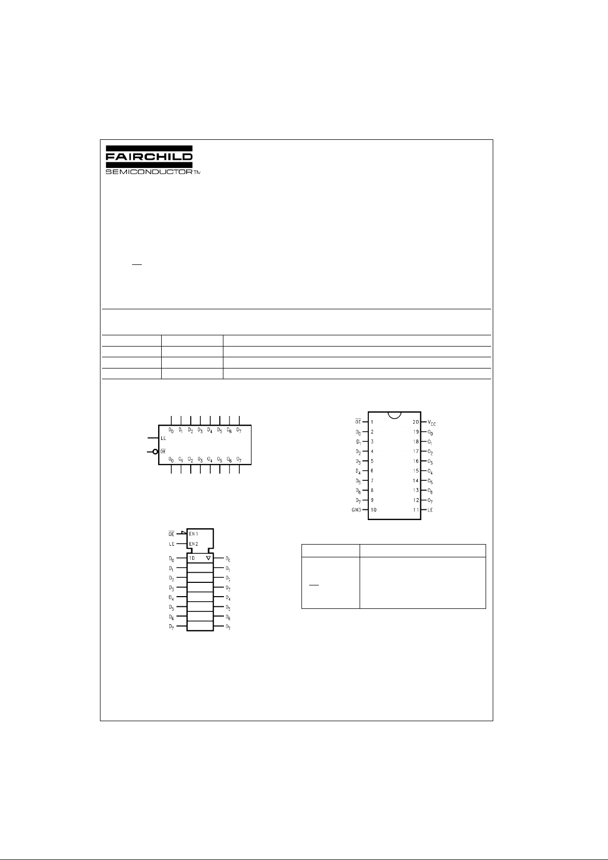
Logic Symbols
IEEE/IEC
Connection Diagram
Pin Descriptions
Order Number Package Number Package Description
74LVX573M M20B 20-Lead Small Outline Integrated Circuit (SOIC), JEDEC MS-013, 0.300” Wide
74LVX573SJ M20D 20-Lead Small Outline Package (SOP), EIAJ TYPE II, 5.3mm Wide
74LVX573MTC MTC20 20-Lead Thin Shrink Small Outline Package (TSSOP), JEDEC MO-153, 4.4mm Wide
Pin Names Description
D
0–D7
Data Inputs
LE Latch Enable Input
OE
3-STATE Output Enable Input
O
0–O7
3-STATE Latch Outputs
Page 2
www.fairchildsemi.com 2
74LVX573
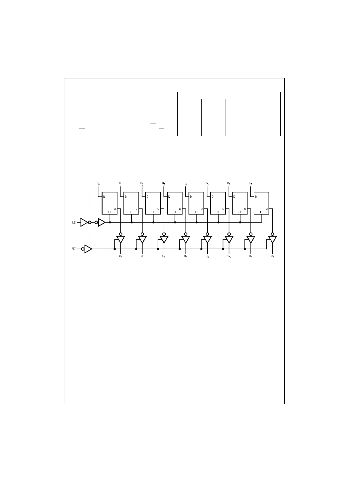
Functional Description
The LVX573 contains eight D-type latches. When the
enable (LE) input is HIGH, data on the D
n
inputs enters the
latches. In this condition the latches are transpar ent, i.e., a
latch output will change state each time its D input
changes. When LE is LOW the la tches store the information that was pres ent on th e D inp uts a s etup ti me preced ing the HIGH-to-LOW transition of LE. The 3-STATE
buffers are controlled by the Output Enable (OE
) input.
When OE
is LOW, the buffers are enabled. When OE is
HIGH the buffers are in the high imp edance mode but this
does not interfere with entering new data into the latches.
Tr uth Table
H = HIGH Voltage
L = LOW Voltage
Z = High Impedance
X = Immaterial
O0 = Previous O0 before HIGH-to-LOW transition of Lat ch Enable
Logic Diagram
Please note that this diagram is provided o nly f or t he understanding o f lo gic operations and shou ld not be used to estimate propagation delays.
Inputs Outputs
OE
LE D O
n
LHH H
LHL L
LLX O
0
HXX Z
Page 3

3 www.fairchildsemi.com
74LVX573
Absolute Maximum Ratings(Note 1) Recommended Operating
Conditions
(Note 2)
Note 1: The “Absolute Maximum Ratings ” are those val ues beyond w hich
the safety of the device cannot be guaranteed. The device should not be
operated at these limits. The parametric values defined in the Electrical
Characteristics tables are not guaranteed at the absolute maximum ratings.
The “Recommend ed O peratin g Cond itions” t able w ill defin e the condition s
for actual device operation.
Note 2: Unused inputs must be held HIGH or LOW. They may not float.
DC Electrical Characteristics
Noise Characteristics
(Note 3)
Note 3: (Input tr = tf = 3ns)
Supply Voltage (VCC) −0.5V to +7.0V
DC Input Diode Current (I
IK
)
V
I
= −0.5V −20 mA
DC Input Voltage (V
I
) −0.5V to 7V
DC Output Diode Current (I
OK
)
V
O
= −0.5V −20 mA
V
O
= VCC + 0.5V +20 mA
DC Output Voltage (V
O
) −0.5V to VCC + 0.5V
DC Output Source
or Sink Current (I
O
) ±25 mA
DC V
CC
or Ground Current
(I
CC
or I
GND
) ±75 mA
Storage Temperature (T
STG
) −65°C to +150°C
Power Dissipation 180 mW
Supply Voltage (V
CC
) 2.0V to 3.6V
Input Voltage (V
I
) 0V to 5.5V
Output Voltage (V
O
)0V to V
CC
Operating Temperature (TA) −40°C to +85°C
Input Rise and Fall Time (∆t/∆V) 0 ns/V to 100 ns/V
Symbol Parameter
V
CC
TA = +25°CT
A
= −40°C to +85°C
Units Conditions
Min Typ Max Min Max
V
IH
HIGH Level 2.0 1.5 1.5
Input Voltage 3.0 2.0 2.0 V
3.6 2.4 2.4
V
IL
LOW Level 2.0 0.5 0.5
Input Voltage 3.0 0.8 0.8 V
3.6 0.8 0.8
V
OH
HIGH Level 2.0 1.9 2.0 1.9 VIN = VIH or VILIOH = −50 µA
Output Voltage 3.0 2.9 3.0 2.9 V IOH = −50 µA
3.0 2.58 2.48 IOH = −4 mA
V
OL
LOW Level 2.0 0.0 0.1 0.1 VIN = VIH or VILIOL = 50 µA
Output Voltage 3.0 0.0 0.1 0.1 V IOL = 50 µA
3.0 0.36 0.44 IOL = 4 mA
I
OZ
3-STATE Output 3.6 ±0.25 ±2.5 µAVIN = VIH or V
IL
Off-State Current V
OUT
= VCC or GND
I
IN
Input Leakage Current 3.6 ±0.1 ±1.0 µAVIN = 5.5V or GND
I
CC
Quiescent Supply Current 3.6 4.0 40.0 µAVIN = VCC or GND
Symbol Parameter
V
CC
(V)
TA = 25°C
Units
CL (pF)
Typ Limit
V
OLP
Quiet Output Maximum Dynamic V
OL
3.3 0.5 0.8 V 50
V
OLV
Quiet Output Minimum Dynamic V
OL
3.3 −0.5 −0.8 V 50
V
IHD
Minimum HIGH Level Dynamic Input Voltage 3.3 2.0 V 50
V
ILD
Maximum LOW Level Dynamic Input Voltage 3.3 0.8 V 50
Page 4

www.fairchildsemi.com 4
74LVX573
AC Electrical Characteristics
Note 4: Paramete r guaranteed by desig n. t
OSLH
= |t
PLHm
− t
PLHn
|, t
OSHL
= |t
PHLm
− t
PHLn
|.
Capacitance
Note 5: CPD is defined as the value of the internal equivalent capacitance w hic h is calculated from the operating current cons umption without load.
Symbol Parameter
V
CC
(V)
TA = +25°CT
A
= −40°C to +85°C
Units Conditions
Min Typ Max Min Max
t
PLH
Propagation 2.7 7.6 14.5 1.0 17.5
ns
CL = 15 pF
t
PHL
Delay Time 10.1 18.0 1.0 21.0 CL = 50 pF
Dn to O
n
3.3 ± 0.3 5.9 9.3 1.0 11.0 CL = 15 pF
8.4 12.8 1.0 14.5 CL = 50 pF
t
PLH
Propagation 2.7 8.2 15.6 1.0 18.5
ns
CL = 15 pF
t
PHL
Delay Time 10.7 19.1 1.0 22.0 CL = 50 pF
LE to O
n
3.3 ± 0.3 6.4 10.1 1.0 12.0 CL = 15 pF
8.9 13.6 1.0 15.5 CL = 50 pF
t
PZL
3-STATE Output 2.7 7.8 15.0 1.0 18.5
ns
CL = 15 pF, RL = 1 kΩ
t
PZH
Enable Time 10.3 18.5 1.0 22.0 CL = 50 pF, RL = 1 kΩ
3.3 ± 0.3 6.1 9.7 1.0 12.0 CL = 15 pF, RL = 1 kΩ
8.6 13.2 1.0 15.5 CL = 50 pF, RL = 1 kΩ
t
PLZ
3-STATE Output 2.7 12.1 19.1 1.0 22.0
ns
CL = 50 pF, RL = 1 kΩ
t
PHZ
Disable Time 3.3 ± 0.3 10.1 13.6 1.0 15.5 CL = 50 pF, RL = 1 kΩ
t
W
LE Pulse 2.7 6.5 7.5
ns
Width 3.3 ± 0.3 5.0 5.0
t
S
Setup Time 2.7 5.0 5.0
ns
Dn to LE 3.3 ± 0.3 3.5 3.5
t
H
Hold Time 2.7 1.5 1.5
ns
Dn to LE 3.3 ± 0.3 1.5 1.5
t
OSHL
Output to Output 2.7 1.5 1.5
ns
CL = 50 pF
t
OSLH
Skew (Note 4) 2.3 1.5 1.5
Symbol Parameter
TA = +25°CT
A
= −40°C to +85°C
Units
Min Typ Max Min Max
C
IN
Input Capacitance 4 10 10 pF
C
OUT
Output Capacitance 6 pF
C
PD
Power Dissipation 27 pF
Capacitance (Note 5)
Page 5

5 www.fairchildsemi.com
74LVX573
Physical Dimensions inches (millimeters) unless otherwise noted
20-Lead Small Outline Integrated Circuit (SOIC), JEDEC MS-013, 0.300” Wide
Package Number M20B
20-Lead Small Outline Package (SOP), EIAJ TYPE II, 5.3mm Wide
Package Number M20D
Page 6

Fairchild does not assume any responsibility for use of any circuitry described, no circuit patent licenses are implied and Fairchild reserves the right at any time without notice to change said circuitry and specifications.
74LVX573 Low Voltage Octal Latch with 3-ST ATE Outputs
LIFE SUPPORT POLICY
FAIRCHILD’S PRODUCTS ARE NOT AUTHORIZED FOR USE AS CRITICAL COMPONENTS IN LIFE SUPPORT
DEVICES OR SYSTEMS WITHOUT THE EXPRESS WRITTEN APPROVAL OF THE PRESIDENT OF FAIRCHILD
SEMICONDUCTOR CORPORATION. As used herein:
1. Life suppor t de vices o r systems a re devices or syste ms
which, (a) are intended for surgical implant into the
body, or (b) support or sustain life, and (c) whose failure
to perform when properly used in accordance with
instructions for use provided in the labeling, can be reasonably expected to result in a significant inju ry to the
user.
2. A critical compon ent in any componen t of a life su pport
device or system whose failu re to perform can be reasonably expected to ca use the fa i lure of the life su pp ort
device or system, or to affect its safety or effectiveness.
www.fairchildsemi.com
Physical Dimensions inches (millimeters) unless otherwise noted (Continued)
20-Lead Thin Shrink Small Outline Package (TSSOP), JEDEC MO-153, 4.4mm Wide
Package Number MTC20
 Loading...