

Page 1
1/9July 2001
■ HIGH SPEED:
t
PD
= 5.0 ns (TYP.) at VCC = 3.3V
■ 5V TOLERANT INPUTS
■ POWER-DOWN PROTECTION ON INPUTS
■ INPUT VOLTAG E LEVEL:
V
IL
= 0.8V, VIH = 2V at VCC =3V
■ LOW POWER DISSIPATION:
I
CC
= 4 µA (MAX.) at TA=25°C
■ LOW NOISE:
V
OLP
= 0.3V (TYP.) at VCC =3.3V
■ SYMMETRICAL OUTPUT IMPED ANCE:
|I
OH
| = IOL = 4 mA (MIN) at VCC =3V
■ BALANCED PROPAGATION DELAYS:
t
PLH
≅ t
PHL
■ OPERATING VOLTAGE RANGE:
V
CC
(OPR) = 2V to 3.6V (1.2V Data Retention)
■ PIN AND FUNCTION COMPATIBLE WITH
74 SERIES 541
■ IMPROVED LATCH-UP IMMUNITY
DESCRIPTION
The 74LVX541 is a low voltage CMOS OCTAL
BUS BUFFER with 3 STATE OUTPUT NON
INVERTING fabricated with sub-micron silicon
gate and double-layer metal wiring C
2
MOS
technology. It is ideal for low power, battery
operated and low noise 3.3V applications.
The 3 STATE control gate opera tes as two input
AND such that if either G1
or G2 are high, all eight
outputs are in the high impedance state.
In order to enhance PC board layout, the
74VHC541 offers a pinout having inputs and
outputs on opposite sides of the package.
Power down protection is provided on all inputs
and 0 to 7V can be accepted on inputs with no
regard to the supply voltage.
This device can be used to interface 5V to 3V. It
combines high speed performance with the true
CMOS low power consumption.
All inputs and outputs are equipped with
protection circuits against stat ic discharge, giving
them 2KV ESD immunity and transient excess
voltage.
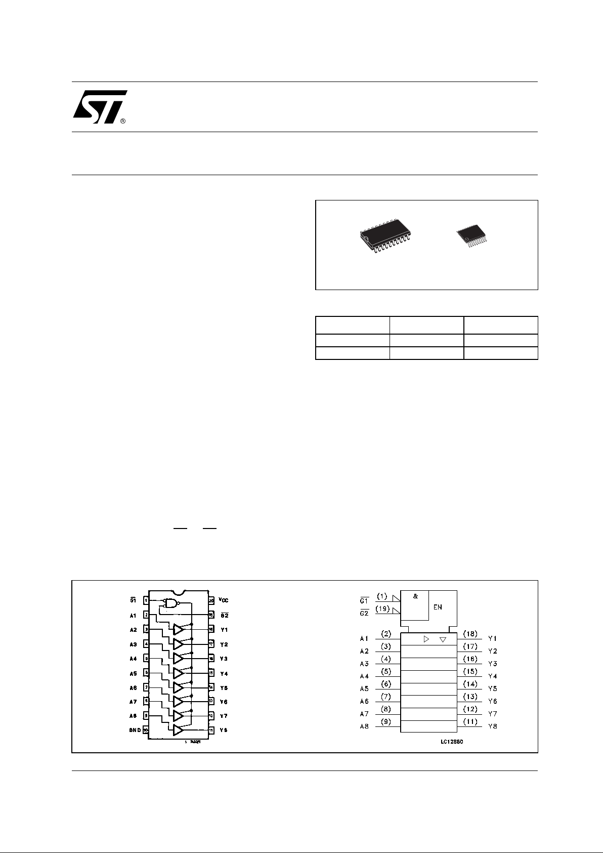
74LVX541
LOW VOLTAGE CMOS OCTAL BUS BUFFER
(3-STATE NON INV.) WITH 5V TOLERANT INPUTS
PIN CONNECTION AND IEC LOGIC SYMBOLS
ORDER CODES
PACKAGE TUBE T & R
SOP 74LVX541M 74LVX541MTR
TSSOP 74LVX541TTR
TSSOPSOP
Page 2
74LVX541
2/9
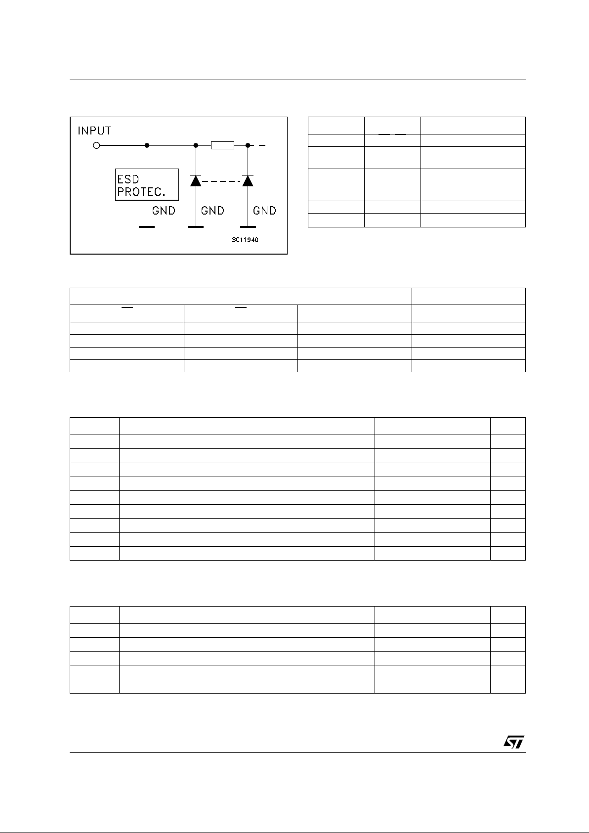
INPUT EQUIVALENT CIRCUIT PIN DESCRIPTION
TRUTH TABLE
X : Don’t Care
Z : High Impedance
ABSOLUTE MAXIMUM RATINGS
Absolute Maximum Ratings are those values beyond which damage to the device may occur. Functional operation under these conditions is
not implied
RECOMMENDED OPERATING CONDITIONS
1) Truth T abl e guarante ed: 1.2V to 3.6V
2) V
IN
from 0.8V to 2.0V
PIN No SYMBOL NAME AND FUNCTION
1, 19 G1
, G2 Output Enable Inputs
2, 3, 4, 5, 6,
7, 8, 9
A1 to A8 Data Inputs
18, 17, 16,
15, 14, 13,
12, 11
Y1 to Y8 Data Outputs
10 GND Ground (0V)
20 V
CC
Positive Supply Voltage
INPUT OUTPUT
G1
G2 An Yn
HXXZ
XHXZ
LLHH
LLLL
Symbol Parameter Value Unit
V
CC
Supply Voltage
-0.5 to +7.0 V
V
I
DC Input Voltage
-0.5 to +7.0 V
V
O
DC Output Voltage -0.5 to VCC + 0.5
V
I
IK
DC Input Diode Current
- 20 mA
I
OK
DC Output Diode Current
± 20 mA
I
O
DC Output Current
± 25 mA
I
CC
or I
GND
DC VCC or Ground Current
± 50 mA
T
stg
Storage Temperature
-65 to +150 °C
T
L
Lead Temperature (10 sec)
300 °C
Symbol Parameter Value Unit
V
CC
Supply Voltage (note 1)
2 to 3.6 V
V
I
Input Voltage
0 to 5.5 V
V
O
Output Voltage 0 to V
CC
V
T
op
Operating Temperature
-55 to 125 °C
dt/dv
Input Rise and Fall Time (note 2) (V
CC
= 3V)
0 to 100 ns/V
Page 3
74LVX541
3/9
DC SPECIFICATIONS
DYNAMIC SWITCHING CHARACTERISTICS
1) Worst c ase package .
2) Max number of outputs defined as (n). Data inp uts are driven 0V to 3.3V, (n-1) outputs switchi ng and one output at GND.
3) Max number of data inputs (n) switching. (n-1) switching 0V to 3.3V. Inputs under test switching: 3.3V to threshold (V
ILD
), 0V to threshold
(V
IHD
), f=1MHz.
Symbol Parameter
Test Condition Value
Unit
V
CC
(V)
T
A
= 25°C
-40 to 85°C -55 to 125°C
Min. Typ. Max. Min. Max. Min. Max.
V
IH
High Level Input
Voltage
2.0 1.5 1.5 1.5
V3.0
2.0 2.0 2.0
3.6
2.4 2.4 2.4
V
IL
Low Level Input
Voltage
2.0 0.5 0.5 0.5
V3.0 0.8 0.8 0.8
3.6 0.8 0.8 0.8
V
OH
High Level Output
Voltage
2.0
IO=-50 µA
1.9 2.0 1.9 1.9
V3.0
I
O
=-50 µA
2.9 3.0 2.9 2.9
3.0
I
O
=-4 mA
2.58 2.48 2.4
V
OL
Low Level Output
Voltage
2.0
I
O
=50 µA
0.0 0.1 0.1 0.1
V3.0
I
O
=50 µA
0.0 0.1 0.1 0.1
3.0
I
O
=4 mA
0.36 0.44 0.55
I
OZ
High Impedance
Output Leakage
Current
3.6
V
I
= VIH or V
IL
VO = VCC or GND
±0.25 ± 2.5 ± 2.5 µA
I
I
Input Leakage
Current
3.6
V
I
= 5V or GND
± 0.1 ± 1 ± 1 µA
I
CC
Quiescent Supply
Current
3.6
V
I
= VCC or GND
44040µA
Symbol Parameter
Test Condition Value
Unit
V
CC
(V)
T
A
= 25°C
-40 to 85°C -55 to 125°C
Min. Typ. Max. Min. Max. Min. Max.
V
OLP
Dynamic Low
Voltage Quiet
Output (note 1, 2)
3.3
C
L
= 50 pF
0.3 0.8
V
V
OLV
-0.8 -0.3
V
IHD
Dynamic High
Voltage Input
(note 1, 3)
3.3 2.0
V
ILD
Dynamic Low
Voltage Input
(note 1, 3)
3.3 0.8
Page 4

74LVX541
4/9
AC ELECTRICAL CHARACTERISTICS (Input tr = tf = 3ns)
1) Skew is defined as the absolute value of the difference between the actual propagation delay for any two outputs of the same device switching in the same direction, either H IGH or LOW
2) Param eter guaran teed by design
(*) Vol tage range is 3. 3V ±
0.3V
CAPACITIVE CHARACTERISTICS
1) CPD is defined as the value of the IC’s internal equivalent capacitance which is calculated from the operating current consumption without
load. (Refer to Test Circuit). Average operating current can be obtained by the following equation. I
CC(opr)
= CPD x VCC x fIN + ICC/8 (per c ircuit )
Symbol Parameter
Test Condition Value
Unit
V
CC
(V)
C
L
(pF)
T
A
= 25°C
-40 to 85°C -55 to 125°C
Min. Typ. Max. Min. Max. Min. Max.
t
PLH
t
PHL
Propagation Delay
Time
2.7
15 6.3 8.3 1.0 10.0 1.0 10.0
ns
2.7
50 9.0 12.0 1.0 15.0 1.0 15.0
3.3
(*)
15 5.0 7.0 1.0 8.5 1.0 8.5
3.3
(*)
50 7.5 10.5 1.0 12.0 1.0 12.0
t
PZL
t
PZH
Output Enable
Time
2.7 15 8.0 12.0 1.0 14.0 1.0 14.0
ns
2.7 50 11.0 15.0 1.0 16.0 1.0 16.0
3.3
(*)
15 6.8 10.8 1.0 12.5 1.0 12.5
3.3
(*)
50 9.3 14.0 1.0 16.0 1.0 16.0
t
PLZ
t
PHZ
Output Disable
Time
2.7 50 12.5 16.5 1.0 19.0 1.0 19.0
ns
3.3
(*)
50 11.2 15.4 1.0 17.5 1.0 17.5
t
OSLH
t
OSHL
Output to Output
Skew Time (note
1,2)
2.7 50 0.5 1.0 1.5 1.5
ns
3.3
(*)
50 0.5 1.0 1.5 1.5
Symbol Parameter
Test Condition Value
Unit
V
CC
(V)
T
A
= 25°C
-40 to 85°C -55 to 125°C
Min. Typ. Max. Min. Max. Min. Max.
C
IN
Input Capacitance
3.3 7101010pF
C
OUT
Output
Capacitance
3.3 9 pF
C
PD
Power Dissipation
Capacitance
(note 1)
3.3
f
IN
= 10MHz
20 pF
Page 5

74LVX541
5/9
TEST CIRCUIT
CL =15/50pF or equivalent (i ncludes jig an d probe capac i tance)
R
L
= R1 = 1KΩ or equivalent
R
T
= Z
OUT
of pulse generator (typically 50Ω)
TEST SWITCH
t
PLH
, t
PHL
Open
t
PZL
, t
PLZ
V
CC
t
PZH
, t
PHZ
GND
Page 6

74LVX541
6/9
WAVEFORM 1 : PROPAGATION DELAYS (f=1MHz; 50% duty cycle)
WAVEFORM 2 : OUTPUT ENABLE AND DISABLE TIMES (f=1MHz; 50% duty cycle)
Page 7

74LVX541
7/9
DIM.
mm. inch
MIN. TYP MAX. MIN. TYP. M AX.
A 2.65 0.104
a1 0.1 0.2 0.004 0.008
a2 2.45 0.096
b 0.35 0.49 0.014 0.019
b1 0.23 0.32 0.009 0.012
C 0.5 0.020
c1 45° (typ.)
D 12.60 13.00 0.496 0.512
E 10.00 10.65 0.393 0.419
e 1.27 0.050
e3 11.43 0.450
F 7.40 7.60 0.291 0.300
L 0.50 1.27 0.020 0.050
M 0.75 0.029
S8° (max.)
SO-20 MECHANICAL DATA
PO13L
Page 8

74LVX541
8/9
DIM.
mm. inch
MIN. TYP MAX. MIN. TYP. M AX.
A 1.2 0.047
A1 0.05 0.15 0.002 0.004 0.006
A2 0.8 1 1.05 0.031 0.039 0.041
b 0.19 0.30 0.007 0.012
c 0.09 0.20 0.004 0.0089
D 6.4 6.5 6.6 0.252 0.256 0.260
E 6.2 6.4 6.6 0.244 0.252 0.260
E1 4.3 4.4 4.48 0.169 0.173 0.176
e 0.65 BSC 0.0256 BSC
K0° 8°0° 8°
L 0.45 0.60 0.75 0.018 0.024 0.030
TSSOP20 MECHANICAL DATA
c
E
b
A2
A
E1
D
1
PIN 1 IDENTIFICATION
A1
L
K
e
0087225C
Page 9

74LVX541
Information furnished is bel ieved to be accurate and reliable. However, STMicroe lectronics assumes no responsibility for the
consequences of use of such information nor for any infringement of patents or other rights of third parties which may result from
its use. No li cense is granted by imp lica tion or otherwise under any patent or patent rig hts of STMicroelectronics. Specificat ions
mentioned in this publication ar e subject to change without notice. This publication supersedes and replaces all information
previously supplied. S TMicroelectronics products are not authorized for use as critica l components in life suppo rt devices or
systems without express written approval of STMicroelectronics.
© The ST logo is a registered trademark of STMicroelectronics
© 2001 STM icroelectronics - Printed in Ital y - All Rights Reserved
STMicr o el ectronics GROUP OF COMPA NI E S
Australi a - Brazil - Chi na - Finland - F rance - Germany - Hong Kon g - India - Italy - Japan - Malay si a - Malta - Morocco
Singapo re - Spain - Sweden - Switzerland - Un i ted Kingdom
© http://www.st.com
9/9
 Loading...