

Page 1
INTEGRATED CIRCUITS
DATA SH EET
74LVC162373A;
74LVCH162373A
16-bit D-type transparent latch;
30 Ω series termination resistors;
5 V tolerant inputs/outputs; 3-state
Product specification
Supersedes data of 1999 Aug 05
2004 Feb 05
Page 2
Philips Semiconductors Product specification
16-bit D-type transparent latch; 30 Ω series termination
resistors; 5 V tolerant inputs/outputs; 3-state
FEATURES
• 5 V tolerant inputs/outputs for interfacing with 5 V logic
• Wide supply voltage range from 1.2 to 3.6 V
• CMOS low power consumption
• MULTIBYTE flow-through standard pin-out architecture
• Low inductance multiple power and ground pins for
minimum noise and ground bounce
• Direct interface with TTL levels
• All data inputs have bushold (74LVCH162373A only)
• High-impedance when VCC=0V
• Complies with JEDEC standard no. 8-1A
• ESD protection:
HBM EIA/JESD22-A114-A exceeds 2000 V
MM EIA/JESD22-A115-A exceeds 200 V.
• Specified from −40 to +85 °C and −40 to +125 °C.
DESCRIPTION
The 74LVC(H)162373A is a 16-bit D-type transparent
latch featuring separate D-type inputs for each latch and
3-state outputs for bus oriented applications. One latch
enable (pin nLE) input and one output enable (pin nOE)
are provided for each octal. Inputs can be driven from
either 3.3 or 5 Vdevices. In 3-state operation, outputs can
handle 5 V. These features allow the use of these devices
in a mixed 3.3 and 5 V environment.
The 74LVC(H)162373A consists of 2 sections of eight
D-typetransparent latches with3-state true outputs.When
pin nLE is HIGH, data at the corresponding data inputs
(pins nDn) enter the latches. In this condition the latches
are transparent, i.e., a latch output will change each time
its corresponding data inputs changes.
When pin nLE is LOW the latches store the information
thatwas presentat the datainputs a set-uptime preceding
the HIGH-to-LOW transition of pin nLE. When pin nOE is
LOW, the contents of the eight latchesare available at the
outputs. When pin nOE is HIGH, the outputs go to the
high-impedance OFF-state. Operation of the nOE input
does not affect the state of the latches.
74LVC162373A;
74LVCH162373A
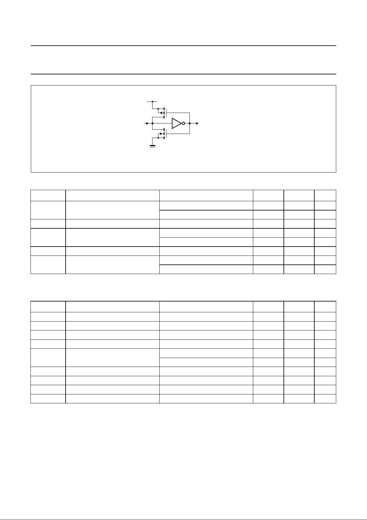
The 74LVCH162373A bushold data inputs eliminates the
need for external pull-up resistors to hold unused inputs.
The 74LVC(H)162373A is designed with 30 Ω series
termination resistorsin both high and low output stages to
reduce line noise.
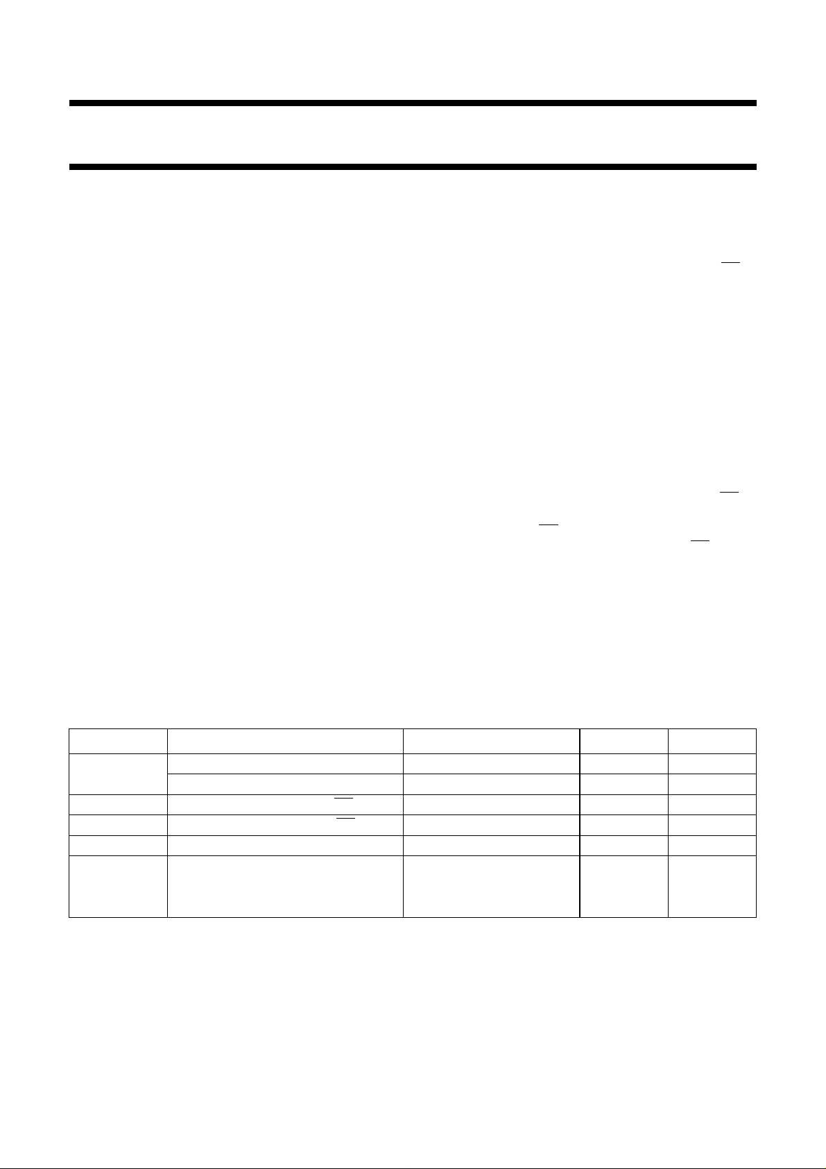
QUICK REFERENCE DATA
GND = 0 V; T
=25°C; tr=tf≤ 2.5 ns
amb
SYMBOL PARAMETER CONDITIONS TYPICAL UNIT
t
PHL/tPLH
propagation delay nDn to nQn CL= 50 pF; VCC= 3.3 V 3.3 ns
propagation delay nLE to nQn CL= 50 pF; VCC= 3.3 V 3.5 ns
t
PZH/tPZL
t
PHZ/tPLZ
C
I
C
PD
3-state output enable time nOE to nQn CL= 50 pF; VCC= 3.3 V 4.0 ns
3-state output disable time nOE to nQn CL= 50 pF; VCC= 3.3 V 3.4 ns
input capacitance 5.0 pF
power dissipation per latch VCC= 3.3 V; notes 1 and 2
outputs enabled 26 pF
outputs disabled 19 pF
Notes
1. C
is used to determine the dynamic power dissipation (PDin µW).
PD
PD=CPD× V
2
× fi× N+Σ(CL× V
CC
2
× fo) where:
CC
fi= input frequency in MHz;
fo= output frequency in MHz;
CL= output load capacitance in pF;
2004 Feb 05 2
Page 3
Philips Semiconductors Product specification
16-bit D-type transparent latch; 30 Ω series termination
resistors; 5 V tolerant inputs/outputs; 3-state
VCC= supply voltage in Volts;
N = total load switching outputs;
Σ(CL× V
2. The condition is VI= GND to VCC.
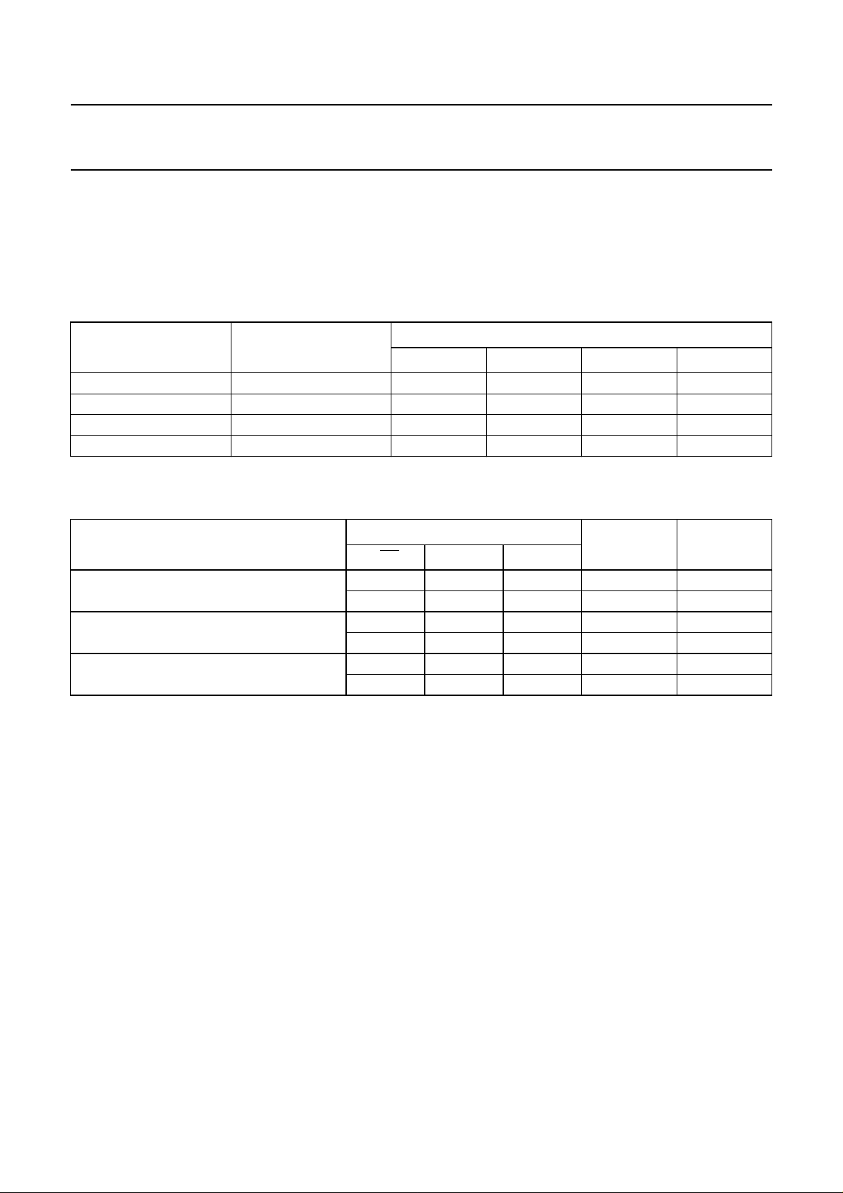
ORDERING INFORMATION
TYPE NUMBER
74LVC162373ADGG −40 to +125 °C 48 TSSOP48 plastic SOT362-1
74LVCH162373ADGG −40 to +125 °C 48 TSSOP48 plastic SOT362-1
74LVC162373ADL −40 to +125 °C 48 SSOP48 plastic SOT370-1
74LVCH162373ADL −40 to +125 °C 48 SSOP48 plastic SOT370-1
FUNCTION TABLE
Per section of eight bits; note 1
Enable and read register (transparent mode) L H L L L
Latch and read register L L l L L
Latch register and disable outputs H L l L Z
2
× fo) = sum of the outputs.
CC
TEMPERATURE
OPERATING MODES
RANGE
PACKAGE
PINS PACKAGE MATERIAL CODE
INPUT
nOE nLE nDn
LHH H H
LLh H H
HLh H Z
74LVC162373A;
74LVCH162373A
INTERNAL
LATCH
OUTPUT nQn
Note
1. H = HIGH voltage level;
h = HIGH voltage level one set-up time prior to the HIGH-to-LOW LE transition;
L = LOW voltage level;
l = LOW voltage level one set-up time prior to the HIGH-to-LOW LE transition;
Z = high-impedance OFF-state.
2004 Feb 05 3
Page 4
Philips Semiconductors Product specification
16-bit D-type transparent latch; 30 Ω series termination
resistors; 5 V tolerant inputs/outputs; 3-state
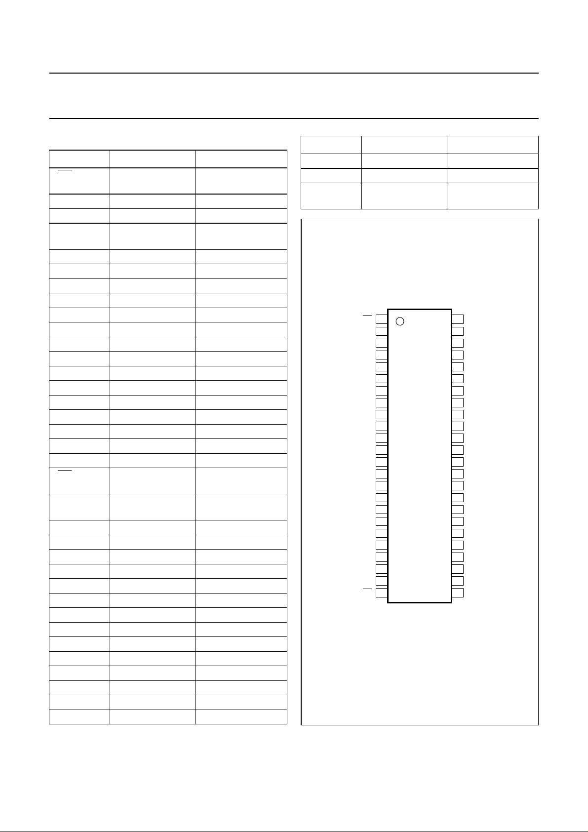
PINNING
SYMBOL PIN DESCRIPTION
1OE 1 output enable input
(active LOW)
1Q0 2 data output
1Q1 3 data output
GND 4, 10, 15, 21, 28,
ground (0 V)
34, 39, 45
1Q2 5 data output
1Q3 6 data output
V
CC
7, 18, 31, 42 supply voltage
1Q4 8 data output
1Q5 9 data output
1Q6 11 data output
1Q7 12 data output
2Q0 13 data output
2Q1 14 data output
2Q2 16 data output
2Q3 17 data output
2Q4 19 data output
2Q5 20 data output
2Q6 22 data output
2Q7 23 data output
2OE 24 output enable input
(active LOW)
2LE 25 latch enable input
(active HIGH)
2D7 26 data input
2D6 27 data input
2D5 29 data input
2D4 30 data input
2D3 32 data input
2D2 33 data input
2D1 35 data input
2D0 36 data input
1D7 37 data input
1D6 38 data input
1D5 40 data input
1D4 41 data input
1D3 43 data input
1D2 44 data input
SYMBOL PIN DESCRIPTION
1D1 46 data input
1D0 47 data input
1LE 48 latch enable input
1OE
1Q0
1Q1
GND
1Q2
1Q3
V
CC
1Q4
1Q5
GND
1Q6
1Q7
2Q0
2Q1
GND
2Q2
2Q3
V
CC
2Q4
2Q5
GND
2Q6
2Q7
2OE
Fig.1 Pin configuration SSOP48 and TSSOP48.
74LVC162373A;
74LVCH162373A
(active HIGH)
1
2
3
4
5
6
7
8
9
10
11
12
162373A
13
14
15
16
17
18
19
20
21
22
23
24
001aaa336
48
1LE
47
1D0
46
1D1
45
GND
44
1D2
43
1D3
V
42
CC
41
1D4
40
1D5
39
GND
38
1D6
37
1D7
36
2D0
35
2D1
34
GND
33
2D2
32
2D3
V
31
CC
30
2D4
29
2D5
28
GND
27
2D6
26
2D7
25
2LE
2004 Feb 05 4
Page 5
Philips Semiconductors Product specification
16-bit D-type transparent latch; 30 Ω series termination
resistors; 5 V tolerant inputs/outputs; 3-state
handbook, full pagewidth
1LE
1OE
Q
D
LATCH
1
LE LE
to 7 other channels
1Q01D0
2LE
2OE
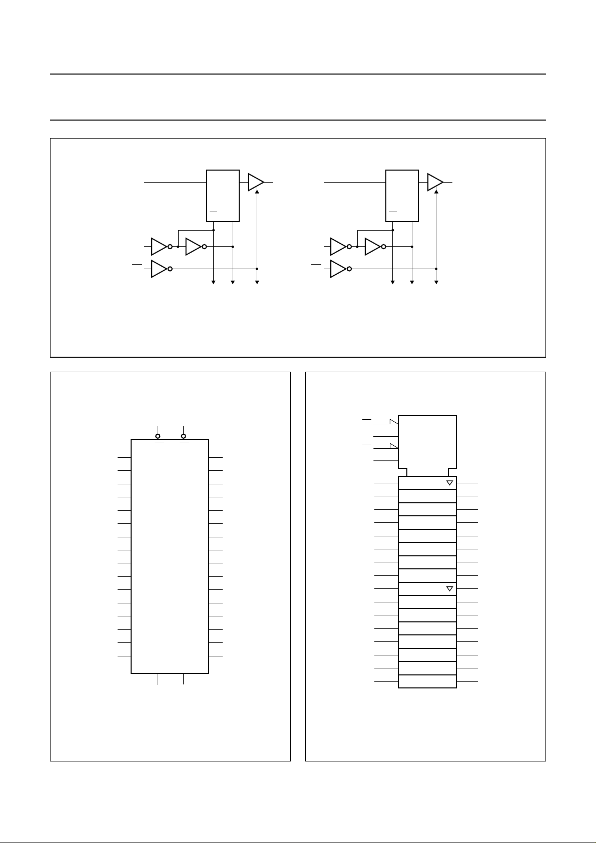
Fig.2 Logic diagram.
74LVC162373A;
74LVCH162373A
Q
D
LATCH
9
LE LE
to 7 other channels
2Q02D0
MGU769
1
24
1OE
2OE
47
1D0
46
1D1
44
1D2
43
1D3
41
1D4
1D5
40
1D6
38
1D7
37
2D0
36
2D1
35
2D2
33
2D3
32
2D4
30
2D5
29
2D6
27
2D7
26
1LE 2LE
48 25
1Q0
1Q1
1Q2
1Q3
1Q4
1Q5
1Q6
1Q7
2Q0
2Q1
2Q2
2Q3
2Q4
2Q5
2Q6
2Q7
2
3
5
6
8
9
11
12
13
14
16
17
19
20
22
23
mgu768
1OE
1LE
2OE
2LE
1D0
1D1
1D2
1D3
1D4
1D5
1D6
1D7
2D0
2D1
2D2
2D3
2D4
2D5
2D6
2D7
1
48
24
25
47
46
44
43
41
40
38
37
36
35
33
32
30
29
27
26
1EN
C3
2EN
C4
3D
4D 2
mgu770
2
1
1Q0
3
1Q1
5
1Q2
6
1Q3
8
1Q4
9
1Q5
11
1Q6
12
1Q7
13
2Q0
14
2Q1
16
2Q2
17
2Q3
19
2Q4
20
2Q5
22
2Q6
23
2Q7
Fig.3 Logic symbol.
2004 Feb 05 5
Fig.4 Logic symbol (IEEE/IEC).
Page 6
Philips Semiconductors Product specification
16-bit D-type transparent latch; 30 Ω series termination
resistors; 5 V tolerant inputs/outputs; 3-state
input
V
CC
to internal circuit
MNA428
handbook, halfpage
74LVC162373A;
74LVCH162373A
Fig.5 Bushold circuit.
RECOMMENDED OPERATING CONDITIONS
SYMBOL PARAMETER CONDITIONS MIN. MAX. UNIT
V
CC
supply voltage for maximum speed performance 2.7 3.6 V
for low-voltage applications 1.2 3.6 V
V
I
V
O
input voltage 0 5.5 V
output voltage output HIGH or LOW state 0 V
CC
V
output 3-state 0 5.5 V
T
amb
tr,t
f
operating ambient temperature in free-air −40 +125 °C
input rise and fall times VCC= 1.2 to 2.7 V 0 20 ns/V
VCC= 2.7 to 3.6 V 0 10 ns/V
LIMITING VALUES
In accordance with the Absolute Maximum Rating System (IEC 60134); voltages are referenced to GND (ground = 0 V).
SYMBOL PARAMETER CONDITIONS MIN. MAX. UNIT
V
CC
I
IK
V
I
I
OK
V
O
supply voltage −0.5 +6.5 V
input diode current VI<0 −−50 mA
input voltage note 1 −0.5 +6.5 V
output diode current VO>VCC or VO<0 −±50 mA
output voltage output HIGH or LOW state; note 1 −0.5 VCC+ 0.5 V
output 3-state; note 1 −0.5 +6.5 V
I
O
ICC, I
T
stg
P
tot
GND
output source or sink current VO=0toV
CC
−±50 mA
VCC or GND current −±100 mA
storage temperature −65 +150 °C
power dissipation T
= −40 to +125 °C; note 2 − 500 mW
amb
Notes
1. The input and output voltage ratings may be exceeded if the input and output current ratings are observed.
2. Above 60 °C the value of P
derates linearly with 5.5 mW/K.
tot
2004 Feb 05 6
Page 7
Philips Semiconductors Product specification
16-bit D-type transparent latch; 30 Ω series termination
resistors; 5 V tolerant inputs/outputs; 3-state
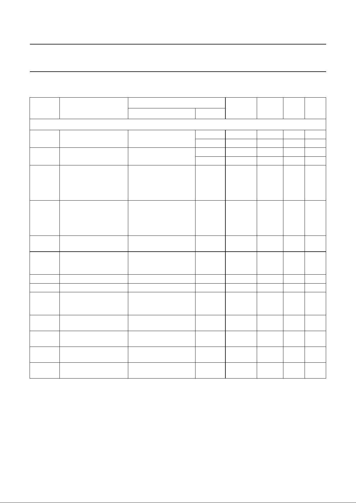
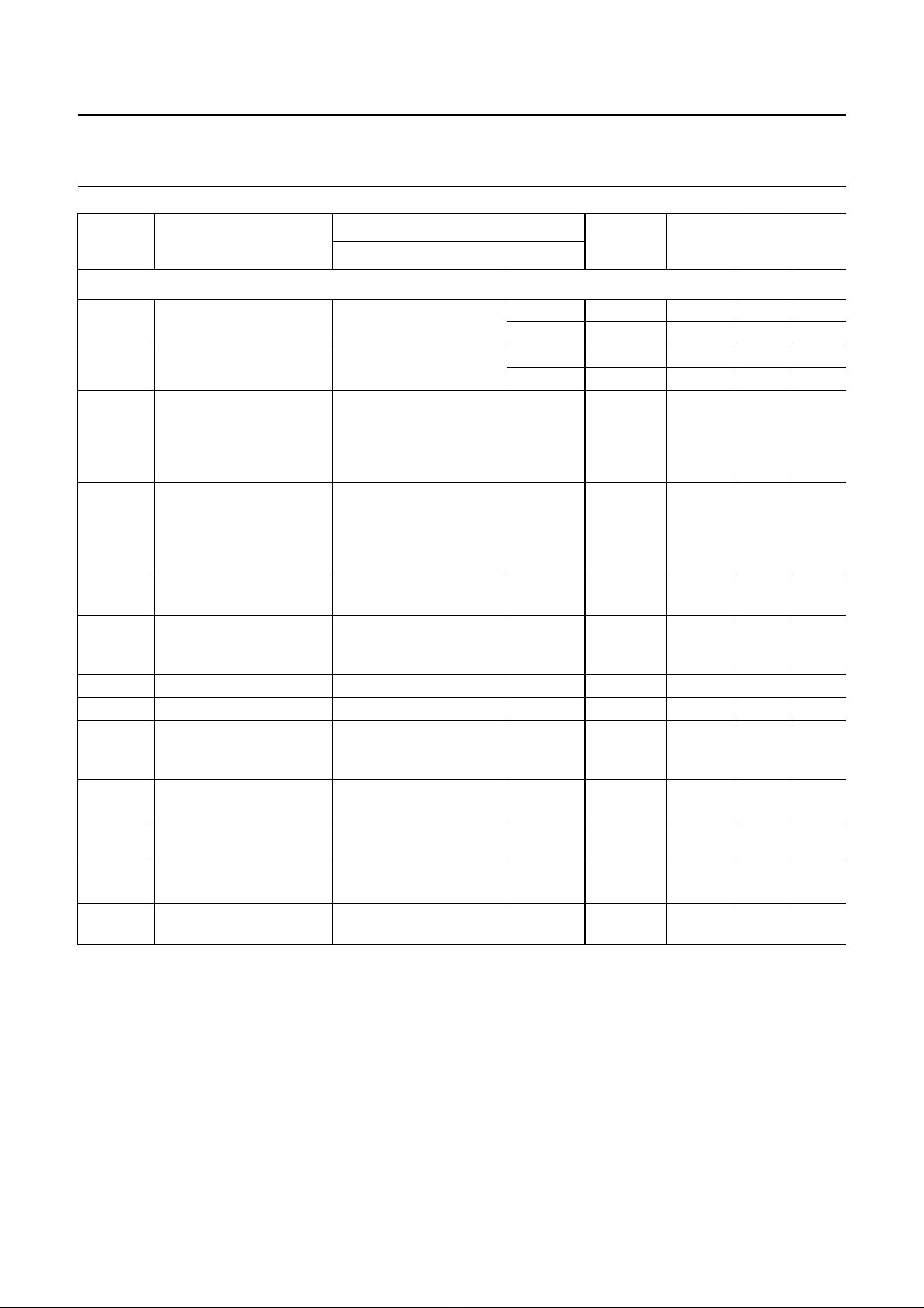
DC CHARACTERISTICS
At recommended operating conditions; voltages are referenced to GND (ground = 0 V).
SYMBOL PARAMETER
T
= −40 to +85 °C; note 1
amb
V
IH
V
IL
V
OH
V
OL
I
LI
I
OZ
HIGH-level input voltage 1.2 V
LOW-level input voltage 1.2 −−GND V
HIGH-level output voltage VI=VIHor V
LOW-level output voltage VI=VIHor V
input leakage current VI= 5.5 Vor GND;
3-state output OFF-state
current
I
I
∆I
off
CC
CC
power-off leakage current VIor VO= 5.5 V 0 −±0.1 ±10 µA
quiescent supply current VI=VCCor GND; IO= 0 3.6 − 0.1 20 µA
additional quiescent
supply current per input
pin
I
BHL
bushold LOW sustaining
current
I
BHH
bushold HIGH sustaining
current
I
BHLO
bushold LOW overdrive
current
I
BHHO
bushold HIGH overdrive
current
note 3
VI=VIHor VIL;
VO= 5.5 Vor GND;
note 3
VI=VCC− 0.6 V; IO= 0 2.7 to 3.6 − 5
VI= 0.8 V; notes 4 and 5 3.0 75 −−µA
VI= 2.0 V; notes 4 and 5 3.0 −75 −−µA
notes 4 and 6 3.6 500 −−µA
notes 4 and 6 3.6 −500 −−µA
TEST CONDITIONS
MIN. TYP. MAX. UNIT
OTHER VCC (V)
CC
2.7 to 3.6 2.0 −−V
2.7 to 3.6 −−0.8 V
IL
IO= −100 µA 2.7 to 3.6 VCC− 0.2 V
IO= −6 mA 2.7 VCC− 0.5 −−V
IO= −12 mA 3.0 VCC− 0.8 −−V
IL
IO= 100 µA 2.7 to 3.6 − GND
IO= 6 mA 2.7 −−0.40 V
IO= 12 mA 3.0 −−0.55 V
3.6 −±0.1 ±5 µA
3.6 −±0.1 ±5 µA
74LVC162373A;
74LVCH162373A
−−V
(2)
(2)
− V
0.20 V
500 µA
CC
(2)
2004 Feb 05 7
Page 8
Philips Semiconductors Product specification
16-bit D-type transparent latch; 30 Ω series termination
resistors; 5 V tolerant inputs/outputs; 3-state
SYMBOL PARAMETER
T
= −40 to +125 °C
amb
V
IH
V
IL
V
OH
V
OL
I
LI
I
OZ
HIGH-level input voltage 1.2 V
LOW-level input voltage 1.2 −−GND V
HIGH-level output voltage VI=VIHor V
LOW-level output voltage VI=VIHor V
input leakage current VI= 5.5 Vor GND;
3-state output OFF-state
current
I
I
∆I
off
CC
CC
power off leakage current VIor VO= 5.5 V 0 −−±20 µA
quiescent supply current VI=VCCor GND; IO= 0 3.6 −−80 µA
additional quiescent
supply current per input
pin
I
BHL
bushold LOW sustaining
current
I
BHH
bushold HIGH sustaining
current
I
BHLO
bushold LOW overdrive
current
I
BHHO
bushold HIGH overdrive
current
note 3
VI=VIHor VIL;
VO= 5.5 Vor GND;
note 3
VI=VCC− 0.6 V; IO= 0 2.7 to 3.6 −−5000 µA
VI= 0.8 V; notes 4 and 5 3.0 60 −−µA
VI= 2.0 V; notes 4 and 5 3.0 −60 −−µA
notes 4 and 6 3.6 500 −−µA
notes 4 and 6 3.6 −500 −−µA
TEST CONDITIONS
OTHER V
CC
(V)
2.7 to 3.6 2.0 −−V
2.7 to 3.6 −−0.8 V
IL
IO= −100 µA 2.7 to 3.6 VCC− 0.3 −−V
IO= −6 mA 2.7 VCC− 0.65 −−V
IO= −12 mA 3.0 VCC− 1 −−V
IL
IO= 100 µA 2.7 to 3.6 −−0.3 V
IO= 6 mA 2.7 −−0.6 V
IO= 12 mA 3.0 −−0.8 V
3.6 −−±20 µA
3.6 −−±20 µA
74LVC162373A;
74LVCH162373A
MIN. TYP. MAX. UNIT
CC
−−V
Notes
1. All typical values are measured at T
amb
=25°C.
2. Measured at VCC= 3.3 V.
3. For bushold parts, the bushold circuit is switched off when VI>VCC allowing 5.5 V on the input pin.
4. Validfor datainputsof busholdparts (LVCH162373A) only.For data inputsonly; control inputsdo not havea bushold
circuit.
5. The specified sustaining current at the data inputs holds the input below the specified VI level.
6. The specified overdrive current at the data input forces the data input to the opposite logic input state.
2004 Feb 05 8
Page 9
Philips Semiconductors Product specification
16-bit D-type transparent latch; 30 Ω series termination
resistors; 5 V tolerant inputs/outputs; 3-state
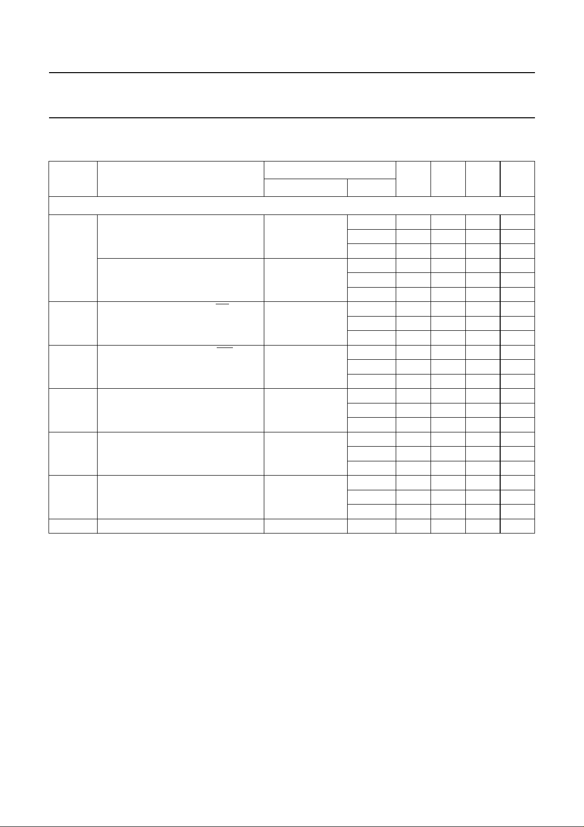
AC CHARACTERISTICS
GND = 0 V; tr=tf≤ 2.5 ns; CL= 50 pF; RL= 500 Ω.
SYMBOL PARAMETER
T
= −40 to +85 °C; note1
amb
t
PHL/tPLH
propagation delay nDn to nQn see Fig 6 and 10 1.2 − 12 − ns
propagation delay nLE to nQn see Fig 7 and 10 1.2 − 14 − ns
t
PZH/tPZL
t
PHZ/tPLZ
t
W
t
su
t
h
t
sk(0)
3-state output enable time nOE to nQn see Fig 8 and 10 1.2 − 18 − ns
3-state output disable time nOE to nQn see Fig 8 and 10 1.2 − 11 − ns
nLE pulse width HIGH see Fig 7 1.2 −−−ns
set-up time nDn to nLE see Fig 9 1.2 −−−ns
hold time nDn to nLE see Fig 9 1.2 −−−ns
skew note 3 3.0 to 3.6 −−1.0 ns
CONDITIONS
WAVEFORMS V
2.7 1.5 − 6.7 ns
3.0 to 3.6 1.0 3.3
2.7 1.5 − 7.0 ns
3.0 to 3.6 1.5 3.5
2.7 1.5 − 7.5 ns
3.0 to 3.6 1.0 4.0
2.7 1.5 − 4.8 ns
3.0 to 3.6 1.5 3.4
2.7 3.0 −−ns
3.0 to 3.6 3.0 2.0
2.7 2.0 −−ns
3.0 to 3.6 2.0 1.0
2.7 0.9 −−ns
3.0 to 3.6 0.9 −1.0
CC
(V)
74LVC162373A;
74LVCH162373A
MIN. TYP. MAX. UNIT
(2)
5.9 ns
(2)
6.1 ns
(2)
6.1 ns
(2)
4.6 ns
(2)
− ns
(2)
− ns
(2)
− ns
2004 Feb 05 9
Page 10
Philips Semiconductors Product specification
16-bit D-type transparent latch; 30 Ω series termination
resistors; 5 V tolerant inputs/outputs; 3-state
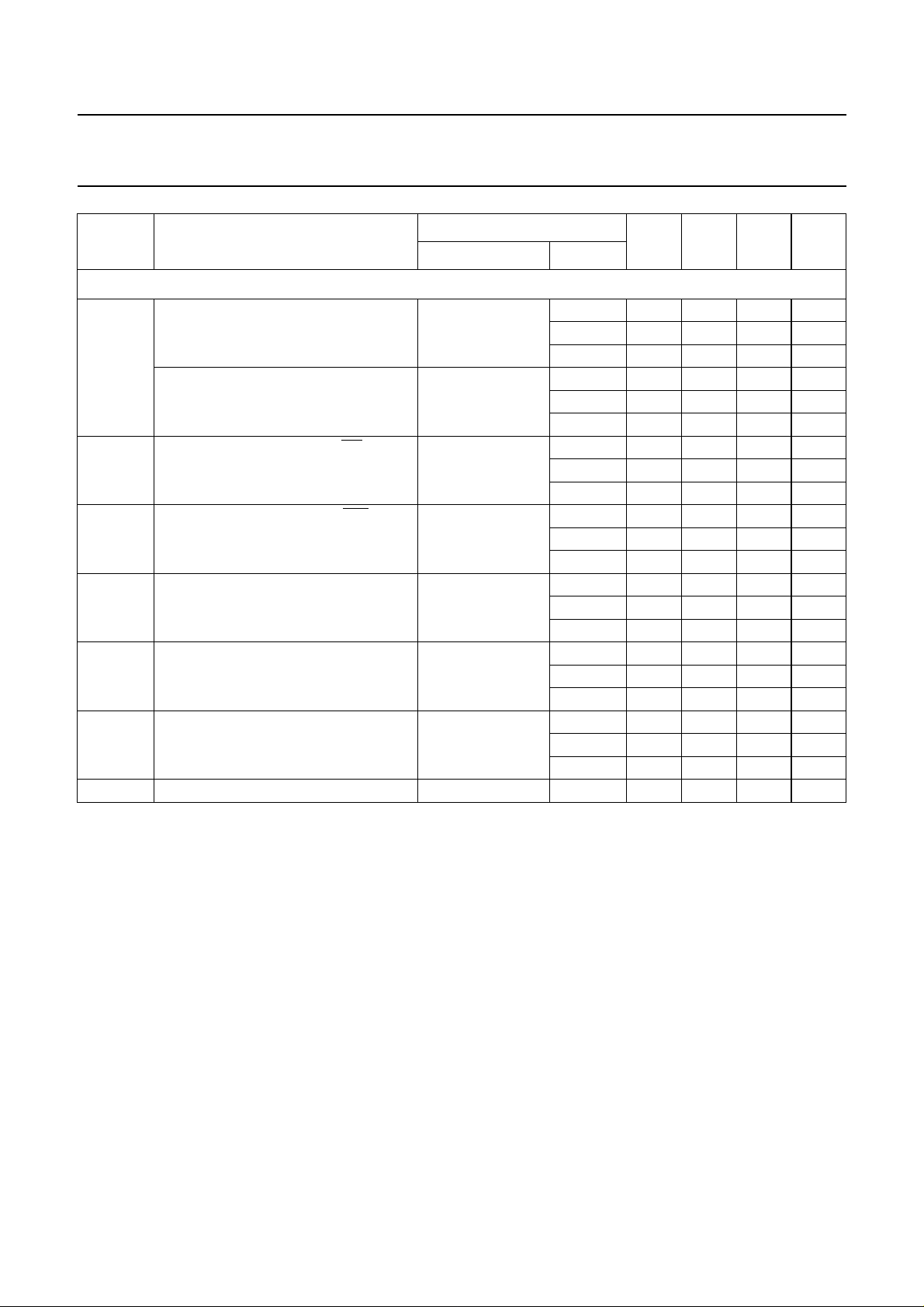
74LVC162373A;
74LVCH162373A
CONDITIONS
SYMBOL PARAMETER
T
= −40 to +125 °C
amb
t
PHL/tPLH
propagation delay nDn to nQn see Fig 6 and 10 1.2 −−−ns
WAVEFORMS V
CC
(V)
MIN. TYP. MAX. UNIT
2.7 1.5 − 8.5 ns
3.0 to 3.6 1.0 − 7.5 ns
propagation delay nLE to nQn see Fig 7 and 10 1.2 −−−ns
2.7 1.5 − 9.0 ns
3.0 to 3.6 1.5 − 8.0 ns
t
PZH/tPZL
3-state output enable time nOE to nQn see Fig 8 and 10 1.2 −−−ns
2.7 1.5 − 9.5 ns
3.0 to 3.6 1.0 − 8.0 ns
t
PHZ/tPLZ
3-state output disable time nOE to nQn see Fig 8 and 10 1.2 −−−ns
2.7 1.5 − 6.0 ns
3.0 to 3.6 1.5 − 6.0 ns
t
W
nLE pulse width HIGH see Fig 7 1.2 −−−ns
2.7 3.0 −−ns
3.0 to 3.6 3.0 −−ns
t
su
set-up time nDn to nLE see Fig 9 1.2 −−−ns
2.7 2.0 −−ns
3.0 to 3.6 2.0 −−ns
t
h
hold time nDn to nLE see Fig 9 1.2 −−−ns
2.7 0.9 −−ns
3.0 to 3.6 0.9 −−ns
t
sk(0)
skew note 3 3.0 to 3.6 −−1.5 ns
Notes
1. All typical values are measured at T
amb
=25°C.
2. Measured at VCC= 3.3 V.
3. Skew between any two outputs of the same package switching in the same direction. This parameter is guaranteed
by design.
2004 Feb 05 10
Page 11
Philips Semiconductors Product specification
16-bit D-type transparent latch; 30 Ω series termination
resistors; 5 V tolerant inputs/outputs; 3-state
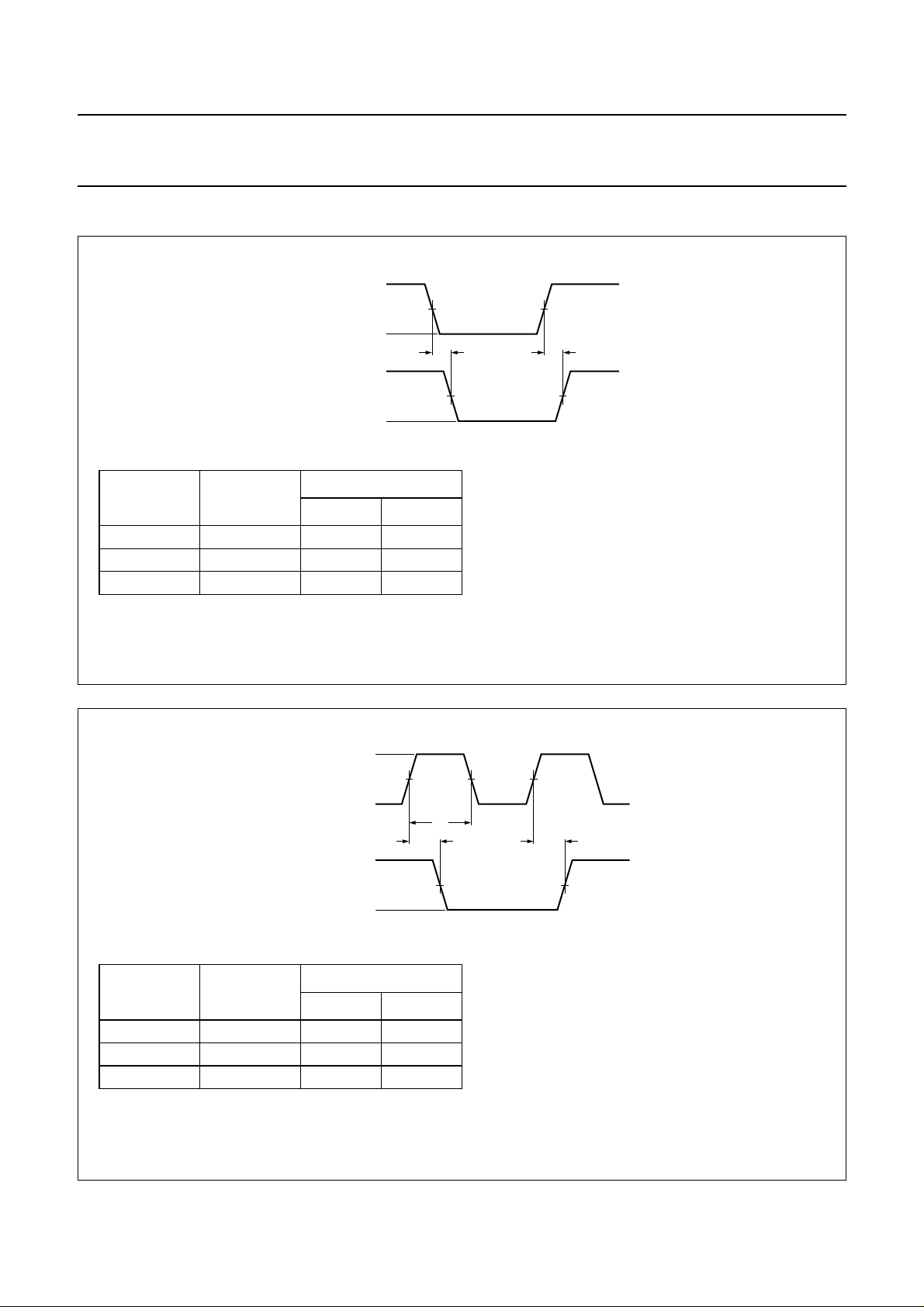
AC WAVEFORMS
V
I
tr=t
V
M
t
PHL
V
M
f
t
PLH
nDn input
GND
V
OH
nQn output
V
OL
INPUT
V
CC
1.2 V 0.5 × V
V
M
CC
V
I
V
CC
≤ 2.5 ns
2.7 V 1.5 V 2.7 V ≤ 2.5 ns
3.0 to 3.6 V 1.5 V 2.7 V ≤ 2.5 ns
74LVC162373A;
74LVCH162373A
mna429
VOL and VOH are the typical output voltage drop that occur with the output load.
Fig.6 Input (nDn) to output (nQn) propagation delays.
V
I
nLE input
nQn output
GND
V
OH
V
OL
V
t
M
PHL
t
W
V
M
INPUT
V
CC
1.2 V 0.5 × V
V
M
CC
V
I
V
CC
tr=t
≤ 2.5 ns
f
2.7 V 1.5 V 2.7 V ≤ 2.5 ns
3.0 to 3.6 V 1.5 V 2.7 V ≤ 2.5 ns
t
PLH
mna430
VOL and VOH are the typical output voltage drop that occur with the output load.
Fig.7 Latch enable input (nLE) pulse width, and the latch enable input to output (nQn) propagation delays.
2004 Feb 05 11
Page 12
Philips Semiconductors Product specification
16-bit D-type transparent latch; 30 Ω series termination
resistors; 5 V tolerant inputs/outputs; 3-state
V
I
nOE input
GND
V
CC
V
OL
V
OH
GND
V
I
V
CC
V
CC
1.2 V 0.5 × V
nQn output
LOW-to-OFF
OFF-to-LOW
nQn output
HIGH-to-OFF
OFF-to-HIGH
V
M
CC
2.7 V 1.5 V 2.7 V ≤ 2.5 ns
3.0 to 3.6 V 1.5 V 2.7 V ≤ 2.5 ns
INPUT
≤ 2.5 ns
V
M
t
PLZ
t
PHZ
outputs
enabled
tr=t
t
PZL
V
M
V
X
t
PZH
V
Y
outputs
disabled
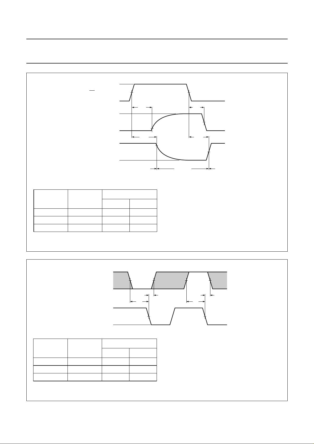
VX=VOL+ 0.3 V at VCC≥ 2.7 V.
f
VX=VOL+ 0.1VCC at VCC< 2.7 V.
VY=VOH− 0.3 V at VCC≥ 2.7 V.
VY=VOH− 0.1VCC at VCC< 2.7 V.
VOL and VOH are the typical output voltage drop that occur with the
output load.
74LVC162373A;
74LVCH162373A
V
M
outputs
enabled
mna432
Fig.8 3-state enable and disable times.
V
I
nDn input
nLE input
GND
GND
V
I
V
M
t
su
INPUT
V
CC
1.2 V 0.5 × V
V
M
CC
V
I
V
CC
tr=t
≤ 2.5 ns
2.7 V 1.5 V 2.7 V ≤ 2.5 ns
3.0 to 3.6 V 1.5 V 2.7 V ≤ 2.5 ns
Fig.9 Data set-up and hold times for the nDn input to the nLE input.
t
h
V
M
f
The shaded areas indicate when the input is permitted to change
for predictable performance.
t
h
t
su
mna431
2004 Feb 05 12
Page 13
Philips Semiconductors Product specification
16-bit D-type transparent latch; 30 Ω series termination
resistors; 5 V tolerant inputs/outputs; 3-state
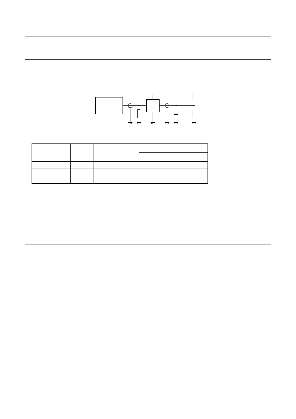
handbook, full pagewidth
V
CC
V
CC
1.2 V V
CC
V
PULSE
GENERATOR
V
I
C
L
50 pF 500 Ω
I
R
L
(1)
D.U.T.
R
T
t
PLH/tPHLtPZH/tPHZtPZL/tPLZ
open GND 2 × V
V
O
V
EXT
2.7 V 2.7 V 50 pF 500 Ω open GND 2 × V
3.0 to 3.6 V 2.7 V 50 pF 500 Ω open GND 2 × V
Note
1. The circuit performs better when RL= 1000 Ω.
V
C
L
EXT
R
R
MNA616
CC
CC
CC
74LVC162373A;
74LVCH162373A
L
L
Definitions for test circuit:
RL= Load resistor.
CL= Load capacitance including jig and probe capacitance.
RT= Termination resistance should be equal to the output impedance Zo of the pulse generator.
Fig.10 Load circuitry for switching times.
2004 Feb 05 13
Page 14
Philips Semiconductors Product specification
16-bit D-type transparent latch; 30 Ω series termination
resistors; 5 V tolerant inputs/outputs; 3-state
PACKAGE OUTLINES
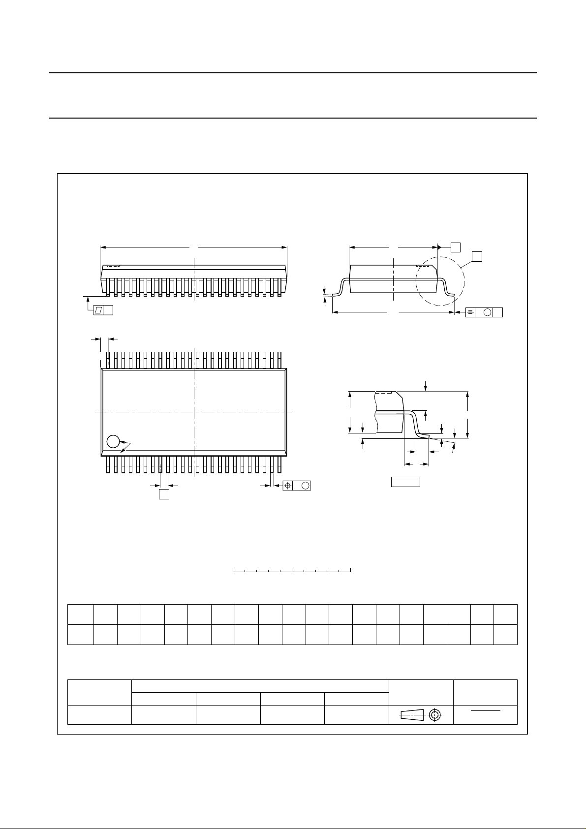
SSOP48: plastic shrink small outline package; 48 leads; body width 7.5 mm
D
c
y
Z
48
25
74LVC162373A;
74LVCH162373A
SOT370-1
E
H
E
A
X
v
M
A
pin 1 index
1
e
0 5 10 mm
DIMENSIONS (mm are the original dimensions)
mm
OUTLINE
VERSION
SOT370-1
A
max.
2.8
0.4
0.2
p
2.35
2.20
IEC JEDEC JEITA
0.25
0.3
0.2
0.22
0.13
MO-118
UNIT A1A2A3b
Note
1. Plastic or metal protrusions of 0.25 mm maximum per side are not included.
(1)E(1)
cD
16.00
15.75
REFERENCES
24
b
p
scale
eHELLpQZywv θ
7.6
0.635 1.4 0.25
7.4
A
2
A
1
w
M
10.4
10.1
1.0
0.6
1.2
1.0
Q
L
p
L
detail X
EUROPEAN
PROJECTION
(A )
3
0.18 0.1
A
θ
(1)
0.85
0.40
ISSUE DATE
99-12-27
03-02-19
o
8
o
0
2004 Feb 05 14
Page 15
Philips Semiconductors Product specification
16-bit D-type transparent latch; 30 Ω series termination
resistors; 5 V tolerant inputs/outputs; 3-state
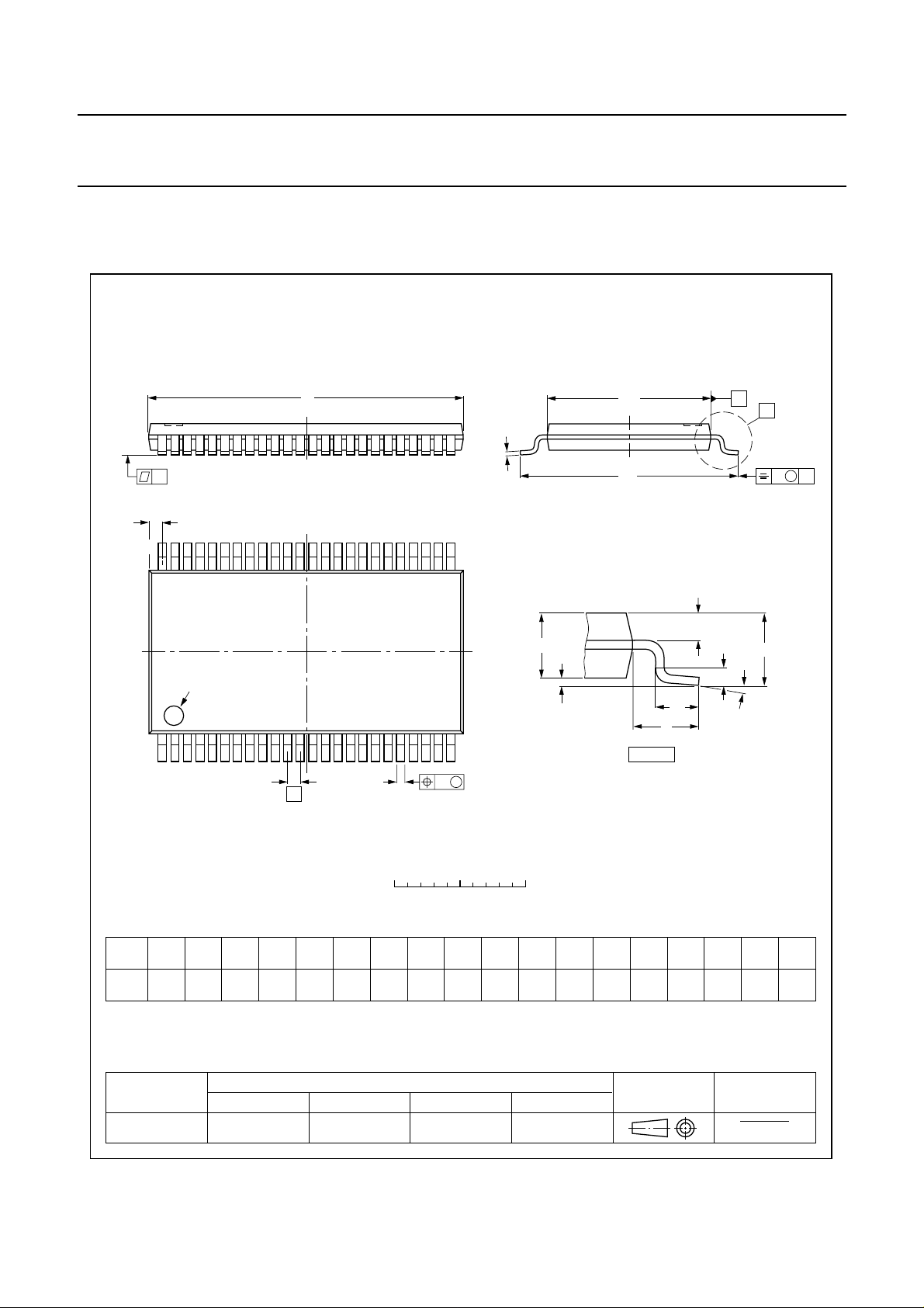
TSSOP48: plastic thin shrink small outline package; 48 leads; body width 6.1 mm
D
c
y
Z
48 25
H
74LVC162373A;
74LVCH162373A
E
E
A
SOT362-1
X
v
M
A
A
2
A
1
pin 1 index
L
p
L
0.50
0.35
detail X
0.08
124
w
b
e
DIMENSIONS (mm are the original dimensions).
mm
A
max.
1.2
0.15
0.05
1.05
0.85
0.25
0.28
0.17
p
cD
0.2
0.2
0.1
0.1
UNIT A1A2A3b
Notes
1. Plastic or metal protrusions of 0.15 mm maximum per side are not included.
2. Plastic interlead protrusions of 0.25 mm maximum per side are not included.
p
0
(1)E(2)
12.6
12.4
M
2.5
scale
eHELLpQZywv θ
6.2
0.5 1 0.25
6.0
8.3
7.9
5 mm
0.8
0.4
Q
(A )
3
A
θ
o
0.8
0.4
8
o
0
0.1
OUTLINE
VERSION
SOT362-1
IEC JEDEC JEITA
REFERENCES
MO-153
2004 Feb 05 15
EUROPEAN
PROJECTION
ISSUE DATE
99-12-27
03-02-19
Page 16

Philips Semiconductors Product specification
16-bit D-type transparent latch; 30 Ω series termination
resistors; 5 V tolerant inputs/outputs; 3-state
DATA SHEET STATUS
LEVEL
I Objective data Development This data sheet contains data from the objective specification for product
II Preliminary data Qualification This data sheet contains data from the preliminary specification.
III Product data Production This data sheet contains data from the product specification. Philips
Notes
1. Please consult the most recently issued data sheet before initiating or completing a design.
2. The product status of the device(s) described in this data sheet may have changed since this data sheet was
3. For data sheets describing multiple typenumbers, thehighest-level productstatus determines the data sheet status.
DATA SHEET
STATUS
published. The latest information is available on the Internet at URL http://www.semiconductors.philips.com.
(1)
PRODUCT
STATUS
(2)(3)
development. Philips Semiconductors reserves the right to change the
specification in any manner without notice.
Supplementary data will be published at a later date. Philips
Semiconductors reserves the right to change the specification without
notice, in order to improve the design and supply the best possible
product.
Semiconductors reserves the right to make changes at any time in order
to improve the design, manufacturing and supply. Relevant changes will
be communicated via a Customer Product/Process Change Notification
(CPCN).
DEFINITION
74LVC162373A;
74LVCH162373A
DEFINITIONS
Short-form specification The data in a short-form
specification is extracted from a full data sheet with the
same type number and title. For detailed information see
the relevant data sheet or data handbook.
Limiting values definition Limiting valuesgiven arein
accordance with the Absolute Maximum Rating System
(IEC 60134). Stress above one or more of the limiting
values may cause permanent damage to the device.
These are stress ratings only and operation of the device
atthese or atanyother conditionsabovethose given inthe
Characteristics sectionsof the specification is not implied.
Exposure to limiting values for extended periods may
affect device reliability.
Application information Applications that are
described herein for any of these products are for
illustrative purposes only. Philips Semiconductors make
norepresentation or warranty thatsuchapplications will be
suitable for the specified use without further testing or
modification.
DISCLAIMERS
Life support applications These products are not
designed for use in life support appliances, devices, or
systems where malfunction of these products can
reasonably be expectedto resultin personal injury. Philips
Semiconductorscustomersusing or sellingtheseproducts
for use in such applications do so at their own risk and
agree to fully indemnify Philips Semiconductors for any
damages resulting from such application.
Right to make changes Philips Semiconductors
reserves the right to make changes in the products including circuits, standard cells, and/or software described or contained herein in order to improve design
and/or performance. When the product is in full production
(status ‘Production’), relevant changes will be
communicated via a Customer Product/Process Change
Notification (CPCN). Philips Semiconductors assumes no
responsibility or liability for the use of any of these
products, conveys no licence or title under any patent,
copyright, or mask work right to these products, and
makes no representations or warranties that these
products are free from patent, copyright, or mask work
right infringement, unless otherwise specified.
2004 Feb 05 16
Page 17

Philips Semiconductors – a w orldwide compan y
Contact information
For additional information please visit http://www.semiconductors.philips.com. Fax: +31 40 27 24825
For sales offices addresses send e-mail to: [email protected].
© Koninklijke Philips Electronics N.V. 2004
All rights are reserved. Reproduction in whole or in part is prohibited without the prior written consent of the copyright owner.
The information presented in this document does not form part of any quotation or contract, is believed to be accurate and reliable and may be changed
without notice. No liability will be accepted by the publisher for any consequence of its use. Publication thereof does not convey nor imply any license
under patent- or other industrial or intellectual property rights.
Printed in The Netherlands R20/02/pp17 Date of release: 2004 Feb 05 Document order number: 9397 750 12674
SCA76
 Loading...