

Page 1

INTEGRATED CIRCUITS
74LV4799
Timer for NiCd and NiMH chargers
Product specification
Supersedes data of 1998 Apr 07
IC24 Data Handbook
1998 Apr 20
Page 2
Philips Semiconductors Product specification
74L V4799Timer for NiCd and NiMH chargers
FEA TURES
•Wide supply voltage range of 0.9 V to 6 V allows 1 to 4-cell
applications
•10 V allowed on special inputs
•Supports virtually all battery chargers, including switched-mode
power supplies
•On-chip timer calculates the actual capacity of the battery by
measuring the charger time, discharge time and self-discharge time
•Automatic switch-over to trickle charge after completion of the
charge time
•Can be adjusted for use with different types of batteries:
– Charge time: 4 to 16 hours
– Discharge time: 15 minutes to 4.7 hours
– Self-discharge time: 50 to 100 days
•Battery status indication included:
– LED output for charging/full indication
– MOLLI
output for battery-low indication
•LED mode select allows two different methods of indication
•Automatic power-ON reset
•Low-power consumption
•Requires only a few peripheral components
•Very accurate on-chip oscillator
•Scan test facilities included
•I
category: non-standard.
CC
APPLICATIONS
•Time-controlled NiCd and NiMH low-current chargers
•Domestic appliances such as rechargeable battery shavers,
electric toothbrushes etc.
•Portable equipment such as notebook PCs, laptop PCs, camera
flash units etc.
•Personal communications like cordless telephones, personal
mobile radios, pagers, etc.
DESCRIPTION
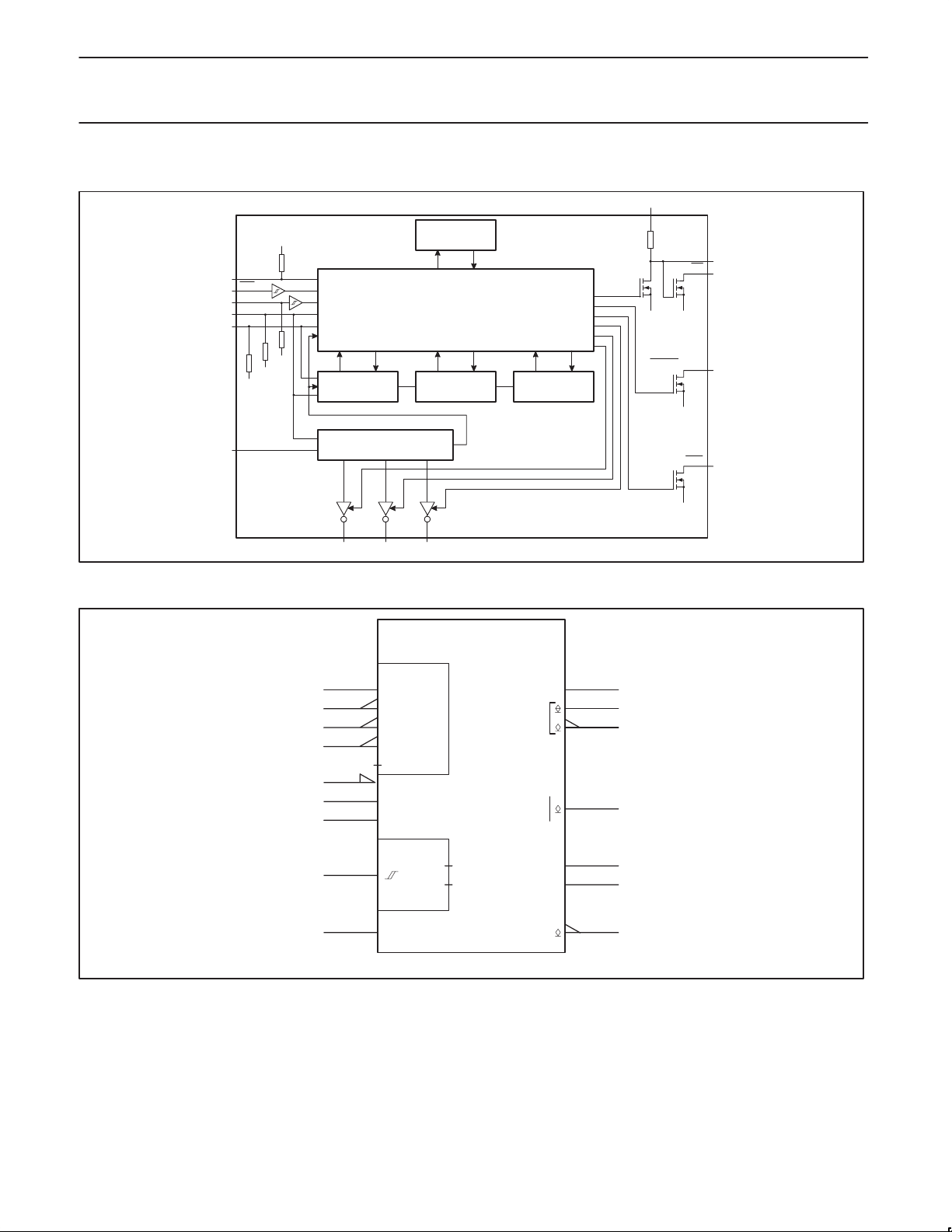
The 74LV4799 is a low-voltage Si-gate CMOS control IC for battery
management. It consists of:
•17-stage divider
•10-stage up/down counter
•Control logic
•Integrated precision oscillator (using external timing components)
•Automatic power-ON reset
•Scan test facilities
•Battery charging/full indication output (LED)
•Battery-low indication output (MOLLI)
•Open-drain-N outputs for driving the load transistor
Battery management with the 74LV4799 is based on the principle of
time measurement. It measures the charge time, discharge time and
self-discharge time by means of a very accurate on-chip oscillator, a
divider and an up/down counter.
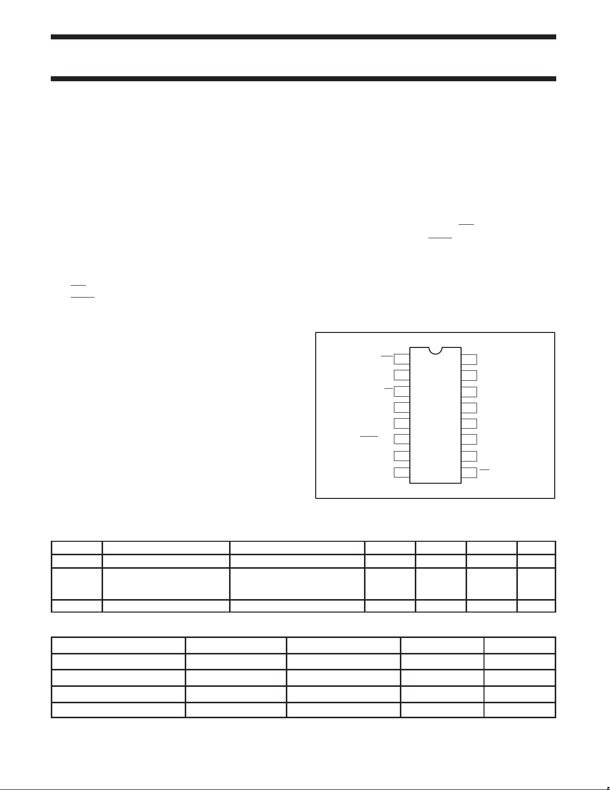
PIN CONFIGURATION
MOLLI
LED
EN
EN
V
PWRS
/SCO
SEL
GND
1
2
3
4
in
5
6
7
8
16
15
14
13
12
11
10
9
SV01643
V
CC
SCI
SCAN
I
OSC
R
S
R
D
R
C
DIS
QUICK REFERENCE DA TA
GND = 0V; T
SYMBOL PARAMETER CONDITIONS TYPICAL TYPICAL TYPICAL UNIT
V
CC
I
CC
f
= 25°C
amb
DC supply voltage 0.9 6.0 V
VCC = 3.3V; self-discharge mode;
= 100 k;
Operating supply current
Oscillator frequency tolerance VCC = 1 to 6 V 7 %
R
s
C
= 220nF
1
36 µA
ORDERING INFORMATION
PACKAGES TEMPERATURE RANGE OUTSIDE NORTH AMERICA NORTH AMERICA CODE
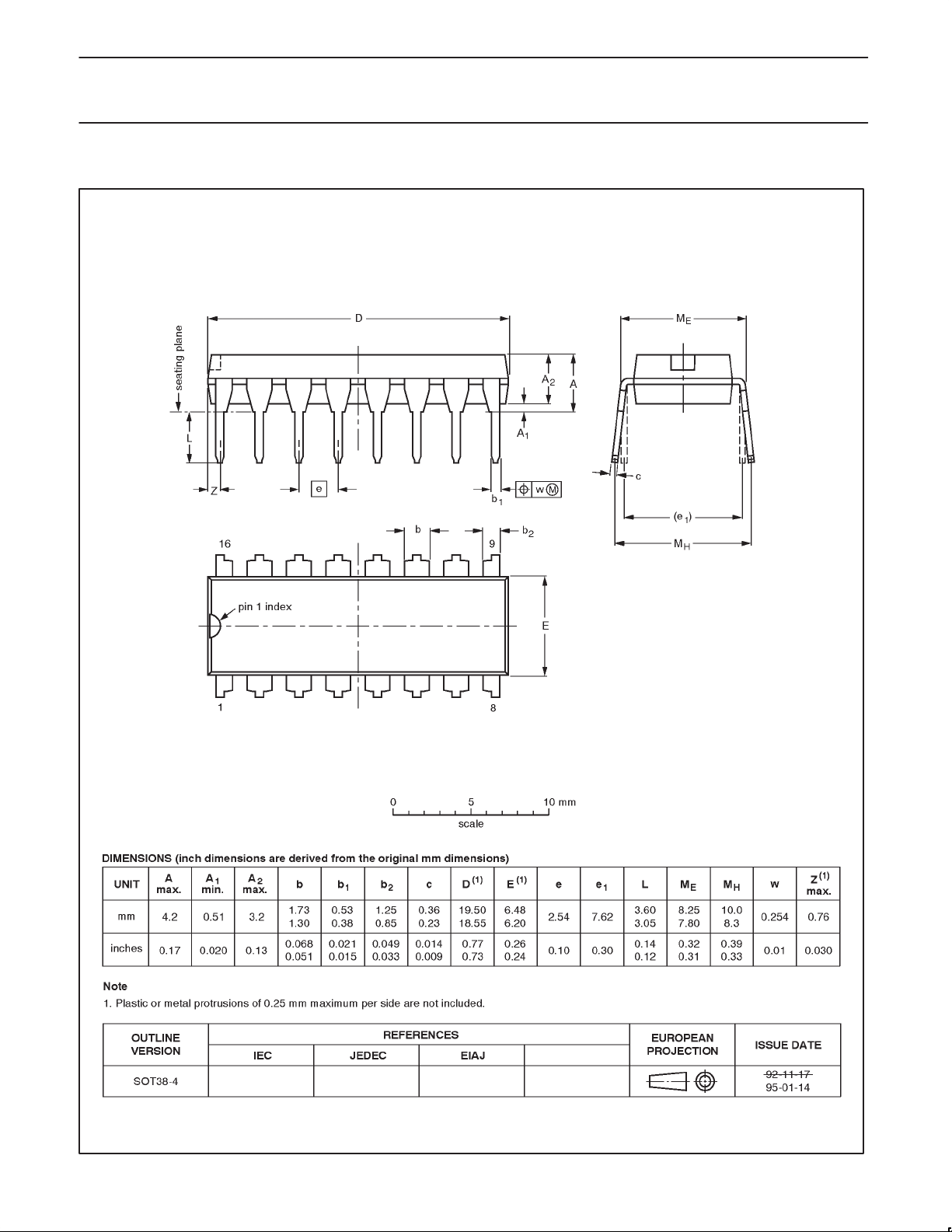
16-Pin Plastic DIL 0°C to +70°C 74LV4799 N 74LV4799 N SOT38-4
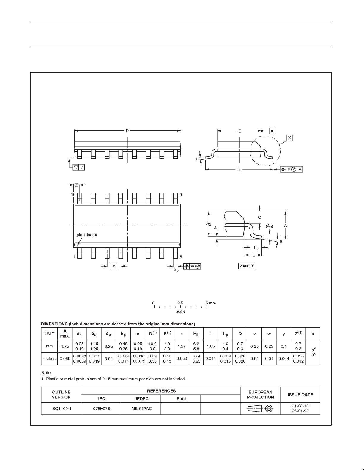
16-Pin Plastic SO 0°C to +70°C 74LV4799 D 74LV4799 D SOT109-1
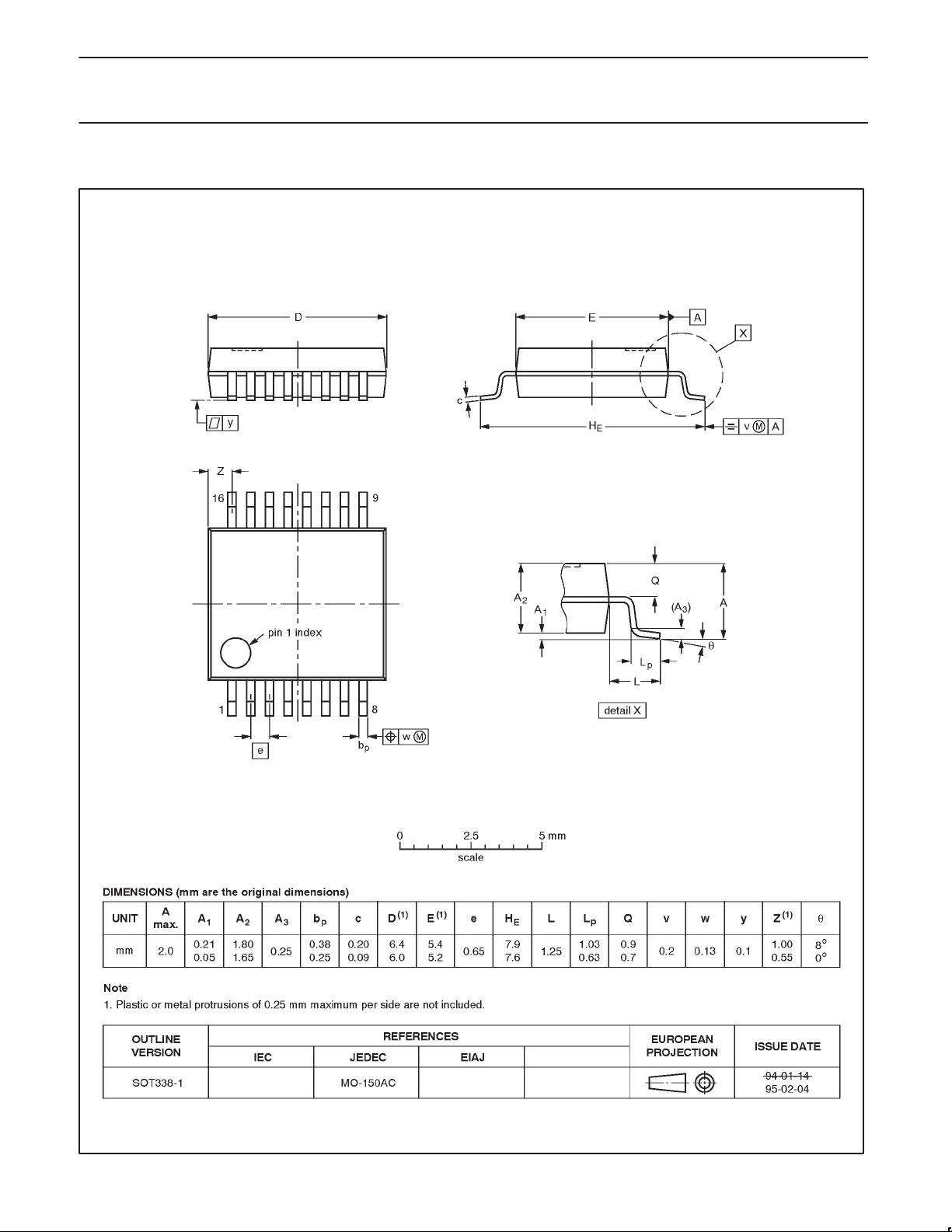
16-Pin Plastic SSOP Type II 0°C to +70°C 74LV4799 DB 74LV4799 DB SOT338-1
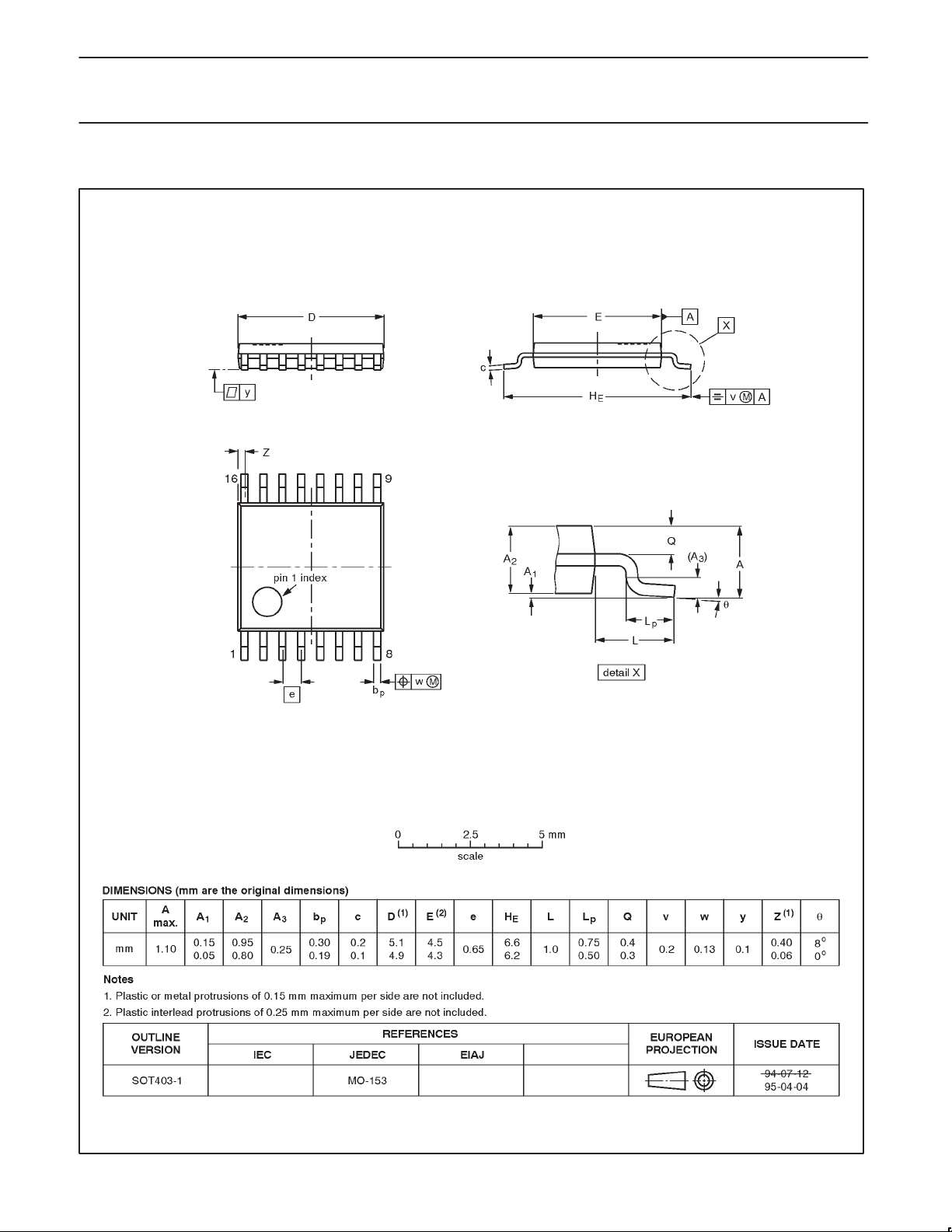
16-Pin Plastic TSSOP Type I 0°C to +70°C 74LV4799 PW 74LV4799PW DH SOT403-1
1998 Apr 20 853-2058 19258
2
Page 3
Philips Semiconductors Product specification
74LV4799Timer for NiCd and NiMH chargers
FUNCTIONAL DIAGRAM
4
V
GND
in
EN
2
EN
3
GND
V
CC
SEL
7
DIS
9
PWRS
5
SCAN
14
SCI
15
POWER–ON
RESET
CONTROL LOGIC
IEC LOGIC SYMBOL
GND
GND
GND
I
OSC
13
3–STAGE
CP
DIVIDER
OSCILLATOR CP
R
C
10 11
13
12
11
10
9
15
14
5–14 STAGE
DIVIDER
R
R
D
S
12
F
BATT. TIMER
G
IOSC
RS
RD
RC
1
DIS
SCI SCO
SCAN/Z1
MOLLI
10–STAGE
UP/DOWN
COUNTER
U+[1]
EN
MOLLI/SCO
4
2
3
6
GND
LED
GND
SV01644
6
1
1998 Apr 20
I=0
5
7
PWRS
SEL
CT=0
U+[2]
0V
LED
16
8
1
SV01645
3
Page 4

Philips Semiconductors Product specification
74LV4799Timer for NiCd and NiMH chargers
PIN DESCRIPTION
PIN NO. SYMBOL NAME AND FUNCTION
1 LED LED driver output pin (active LOW)
2 EN Enable output (active HIGH)
3 EN Enable output (active LOW)
4 V
in
5 PWRS Power sense input
6 MOLLI/SCO More-or-less-low-indication output (active LOW)/scan test output
7 SEL LED mode select input
8 GND Ground (0 V)
9 DIS Discharge input (active LOW)
10 R
11 R
12 R
13 I
C
D
S
OSC
14 SCAN Scan test mode select input (active HIGH)
15 SCI Scan test input
16 V
CC
External power input
External resistor pin 3-State oscillator output (charge)
External resistor pin 3-State output (discharge)
External resistor pin 3-State output (self-discharge)
Oscillator input
Positive supply voltage
Power On Reset.
An automatic Power On Reset initiates the IC when the battery is
discharged and power is connected to the circuit. The initial
condition is the charge mode in which the counter is reset and
counts from zero up to maximum. At start up, the battery therefore
always receives a full charge cycle. When a partially charged battery
is inserted, it may be over-charged during the first cycle. To guard
against this, simply replace the resistor at the R
pin with an NTC
C
type which is in good thermal contact with the battery. If the
temperature of the battery increases, the frequency of the oscillator
also increases to quickly reach a counter full indication and
switch-over to trickle charge. With a battery that is almost
completely discharged, the POR input can also be activated during
discharge or self-discharge. The counter will then be reset to zero.
This is a correct action while returning to the initial condition.
Power-on sensing.
Because this IC supports virtually all battery chargers, the PWRS input
has a broad input frequency spectrum (active HIGH to 100 kHz). A
pull-down circuit at the PWRS input allows detection of the open state
which corresponds to an inactive charger. A HIGH level on the PWRS
input, or an AC signal up to 100 kHz, enables the charge mode.
Start-up with low battery voltage.
Good start-up, even with an un-charged battery, is assured by using
the V
input. The voltage on the VIN input biases the external
IN
bipolar transistors at the EN or EN
output, even if the IC is not yet
functioning. After the battery has received sufficient charge, the
internal control logic takes over control of the EN and EN outputs.
Charge mode.
This mode is selected when PWRS is active (HIGH or pulsed) and
the discharge input DIS
EN
output is LOW initiating continuous charge of the battery. The
is HIGH. The EN output is HIGH, and the
counter then counts from the zero state up to the maximum value.
The clock frequency is determined by the external capacitor and
resistor connected to the R
output. The counter stops when it
C
reaches its maximum value and the EN and EN
outputs switch over
from the continuous charge to the trickle charge mode.
Trickle charge mode.
At the maximum counter value, it is assumed that the battery is fully
charged. The counter stops and remains on this maximum value.
The EN and EN
outputs switch over from the continues charge to
the trickle charge mode. In the trickle charge mode, the average
charge current is reduced to only compensate the self-discharge of
the battery by using the dedicated duty cycle control. The control is
dedicated because it adjusts the duty cycle in inverse proportion to
the load current, resulting in a fixed charger current irrespective of
the kind of charger (e.g. 4-hour or 16-hour charger). In the trickle
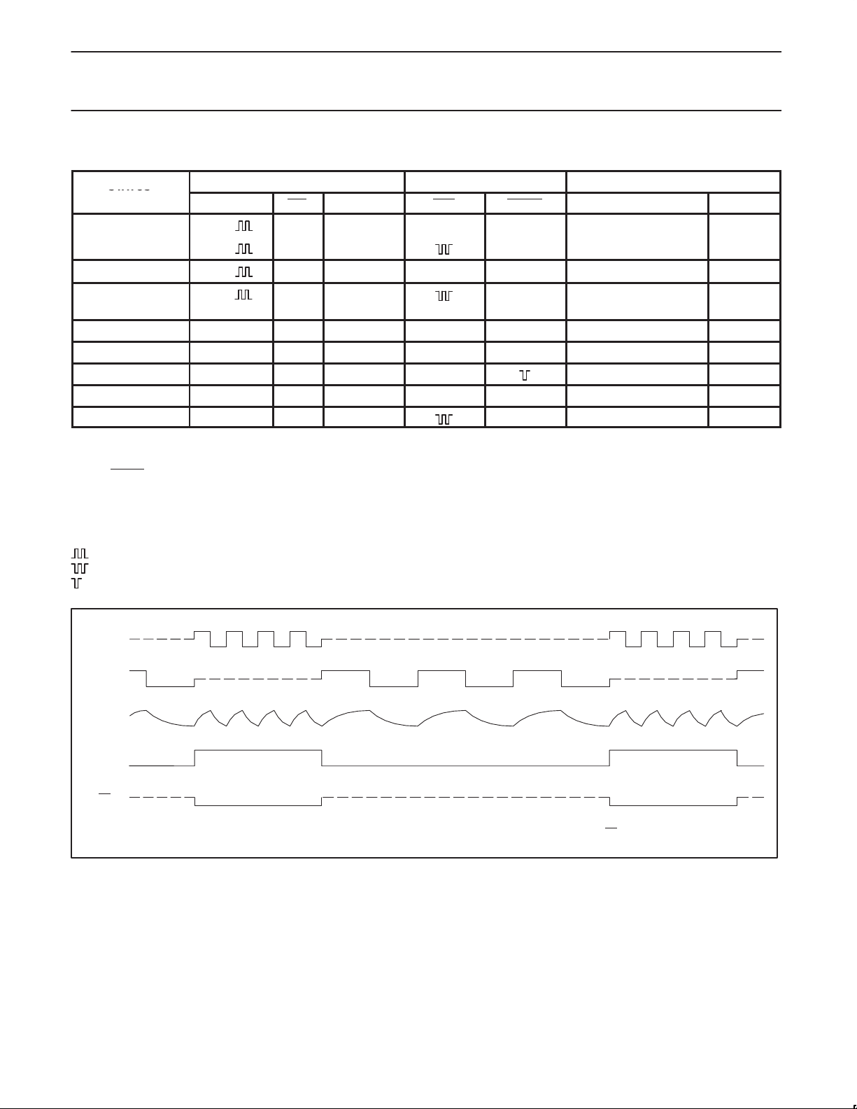
charge mode, the oscillator circuitry alternately generates 4 periods
of R
-C1 time-constant, and 3 periods of the RS -C1 time-constant
C
(See Figure 1).
Discharge mode.
The discharge input (DIS
battery. If DIS
is LOW, the counter counts down. The clock
) is used to detect the discharge of the
frequency is determined by the external capacitor and resistor at the
RD output. If PWRS is inactive (LOW or open), the EN output is
LOW, and the EN
output is in the high impedance OFF-state (no
charge of the battery). This is called the discharge mode. If PWRS is
active, the circuit is in the charge/discharge mode.
Charge/Discharge mode.
If DIS
is LOW and PWRS is active (HIGH or pulsed), the circuit is in
the charge/discharge mode. The counter counts down. The clock
frequency is determined by the external capacitor and resistor tied
at the R
output. The EN output is HIGH, and the EN output is LOW
D
initiating continuous charge of the battery. The battery is therefore
charged and discharged at the same instant, thereby maintaining a
better load condition of the battery.
1998 Apr 20
4
Page 5
Philips Semiconductors Product specification
OPERATING
74LV4799Timer for NiCd and NiMH chargers
Self-discharge mode.
is HIGH and PWRS is inactive (LOW or open), the battery is
If DIS
being neither charged nor discharged. The circuit is in the
self-discharge mode. This mode represents the battery leakage
(self-discharge). The counter counts down. The clock frequency is
determined by the external capacitor and resistor at the R
When the counter reaches the zero state, it stops.
LED mode select.
The LED
charge/full status of the battery. For optimum flexibility, two modes of
operation are built-in.
output drives a battery status LED which indicates the
output.
S
•Mode 1: If SEL is LOW, the LED output is active LOW in the
charge mode, and the LED blinks with a frequency of
about 1 Hz during trickle charge.
•Mode 2: If SEL is HIGH or open, the LED output blinks with a
frequency of about 0.25 Hz in the charge mode, and is
active LOW during trickle charge. In the discharge or
self-discharge mode, the LED
when PWRS is active (HIGH or pulsed). Then, the
battery is charging and discharging simultaneously.
Although the discharge mode is dominant, the LED
output is active when PWRS is also active.
NOTE: The blink frequency depends on the oscillator frequency.
(See application information)
Low indication.
As part of the user interface, the MOLL
battery needs to be charged. MOLLI
Indication (active LOW). The function is as follows: In the discharge
mode, (DIS
reaches the zero state, it stops. If DIS
output gives an output signal of four periods of about one second,
with a 50% duty cycle. This can be used to activate a buzzer. The
MOLLI
PWRS is activated.
Alarm indication.
If an almost completely discharged battery is connected to the
charger, it may not be noticed by the user if the load switch is still
is active LOW), the counter counts down and, when it
output signal of four periods will be interrupted as soon as
output is open except
I output shows when the
stands for More Or Less Low
is switched HIGH, the MOLLI
on. To prevent damaging the battery , an alarm signal on the LED
output will alert the user to switch off the load. The alarm signal is
easily recognized, because the LED
frequency than normal (about 5 Hz instead of 1 Hz). This alarm
indication is only active if the SEL input is HIGH or open. If the SEL
input is LOW, no alarm indication is present, because in many
applications simultaneous charging and discharging is quite
acceptable. (See charge/discharge mode)
Scan test mode.
If the SCAN input (pin 14) is made active HIGH, the circuit is in the
test mode. The tester clock is connected to the I
the scan mode, the on–chip oscillator is bypassed to allow rapid
testing of the divider/counter. The scan test patterns are available on
request. The scan test data is entered serially through the SCI input
(pin 15). The scan out data is present on the MOLLI
(pin 6), which then acts as a scan output.
Remaining energy indication.
The scan test facility can be used as a remaining energy indication
because the value of the counter can be read out at the scan output
(MOLLI
/SCO). This is done by briefly interrupting the normal mode
of operation, putting the circuit in the scan mode, and reading out
the counter value. The circuit then reverts to the normal mode. This
only works correctly with the MOLLI
linked (round coupled loop) and with exactly 49 clock pulses applied
to the I
The serial scan-out data is available on the MOLLI/SCO output. The
value of the counter can be decoded by reading the correct bits.
Details are given later in the section “Application information”.
Output drivers EN and EN
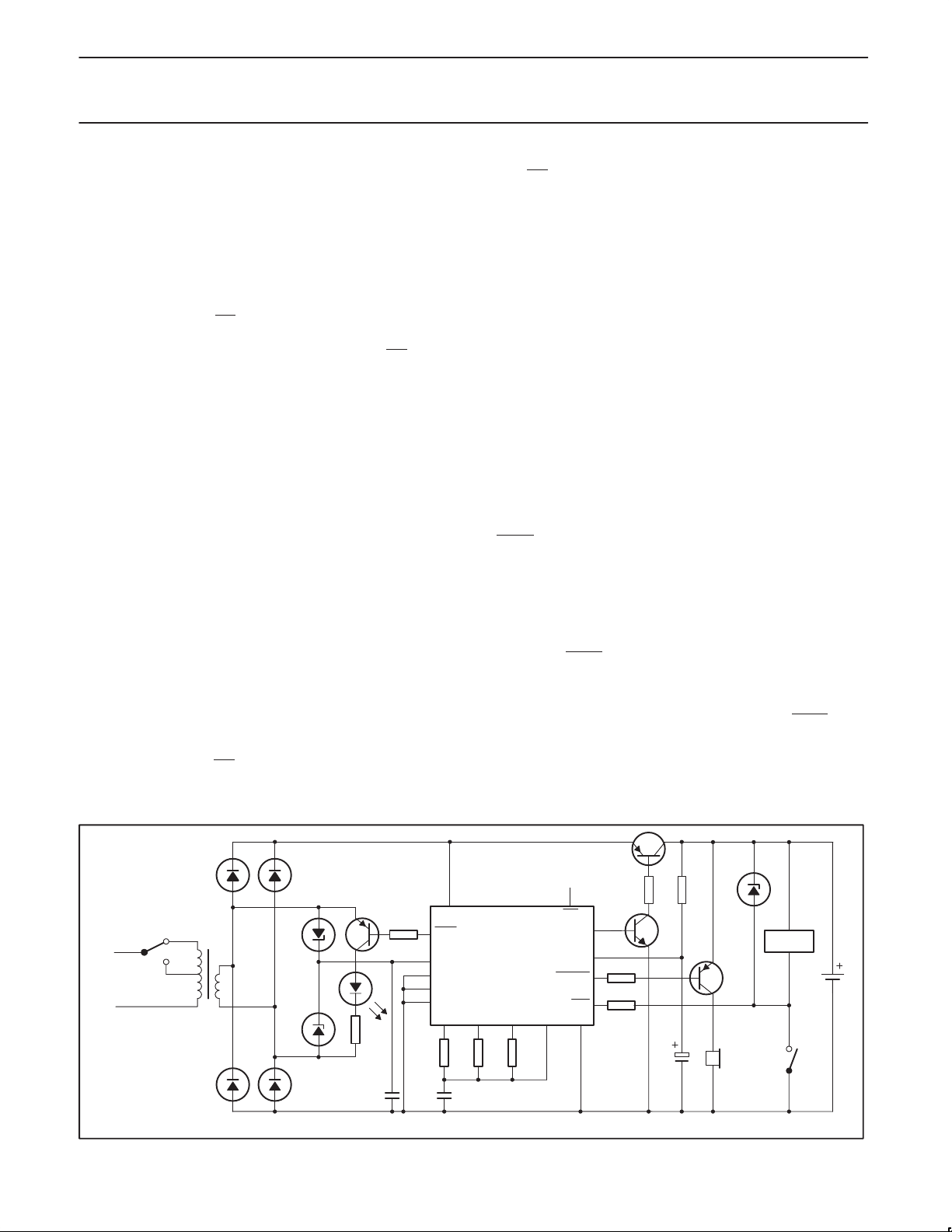
In one-cell battery (low-voltage) applications, the drive from the
ENABLE output (EN
for the external bipolar PNP regulator transistor. The inverse signal has
therefore been made available at the ENABLE output (EN) to drive an
extra bipolar NPN transistor that can provide the base current for the
bipolar PNP regulator transistor as shown in Figure 2.
OSC
input.
) is insufficient to provide the base current directly
output will blink at a higher
/SCO output and SCI input
.
pin (pin 13). In
OSC
/SCO output
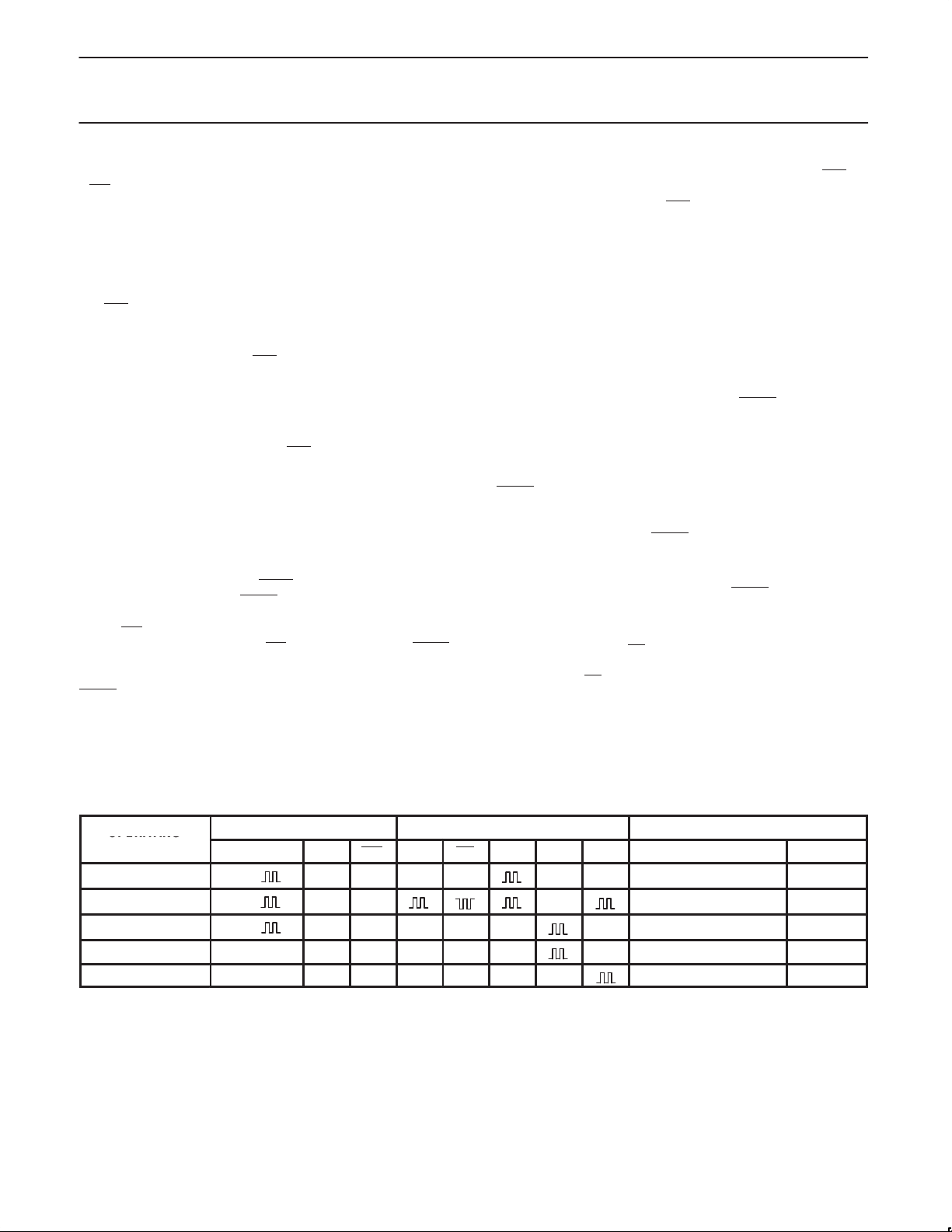
FUNCTION TABLE 1
Charge
Trickle charge
Charge/discharge
Discharge L or open X L L Z Z Z Count down 18 sections ≥ min
Self-discharge L or open X H L Z Z Z Count down 27 sections ≥ min
1998 Apr 20
OPERATING
MODES
INPUTS OUTPUTS DIVIDER/COUNTER
PWRS V
H or
H or
H or
DIS EN EN R
IN
H H H L Z Z Count up 22 sections < max
H H Z Stop max
H L H L Z Z Count down 18 sections ≥ min
5
R
C
R
D
S
MODE VALUE
Page 6
Philips Semiconductors Product specification
STATUS
Ch
Trickle charge
74LV4799Timer for NiCd and NiMH chargers
FUNCTION TABLE 2
STATUS
INDICATION
arge
PWRS DIS SEL
H or
H or
Charge/discharge
H or
H or
H or H H or open L
Discharge L or open L X Z Z Count down > min
Self-discharge L or open H X Z Z Count down > min
Low L or open ↑ X Z Stop min
Low ↑ ↑ X Z Z
Alarm H or L H or open
INPUTS OUTPUTS COUNTER
(1)
LED MOLLI MODE VALUE
H L L Z Count up < max
H H or open Z Count up < max
L L L Z Count down ≥ min
H L
Z
Z
(2)
Z
Stop max
Stop max
Count up ≥ min
Count down ≥ min
NOTES:
1. Don’t change SEL during operation.
2. The MOLLI
function will be interrupted as soon as PWRS is activated.
H = HIGH voltage level
L = LOW voltage level
Z = high impedance OFF-state
X = don’t care
= pulsed (H/L)
= pulsed (Z/L)
= 4 periods of about one second (Z/L)
↑ = LOW-to-HIGH level transition
Z–state
C
S
Operation in the trickle charge mode. The duration of the RC cycle determines the duty cycle of the enable outputs (EN and EN), allowing a dedicated
control. The average trickle charge current will compensate for the self-discharge, independent of the charge current.
Z–state
I
R
R
OSC
EN
EN
Z–state
Z–state
Z–state
SV01646
Figure 1. Trickle charge mode characteristics.
1998 Apr 20
6
Page 7
Philips Semiconductors Product specification
V
Power dissi ation er ackage
for tem erature range: 40 to +125 C
P
y
mW
Pl
(SSOP
TSSOP)
W/K
74LV4799Timer for NiCd and NiMH chargers
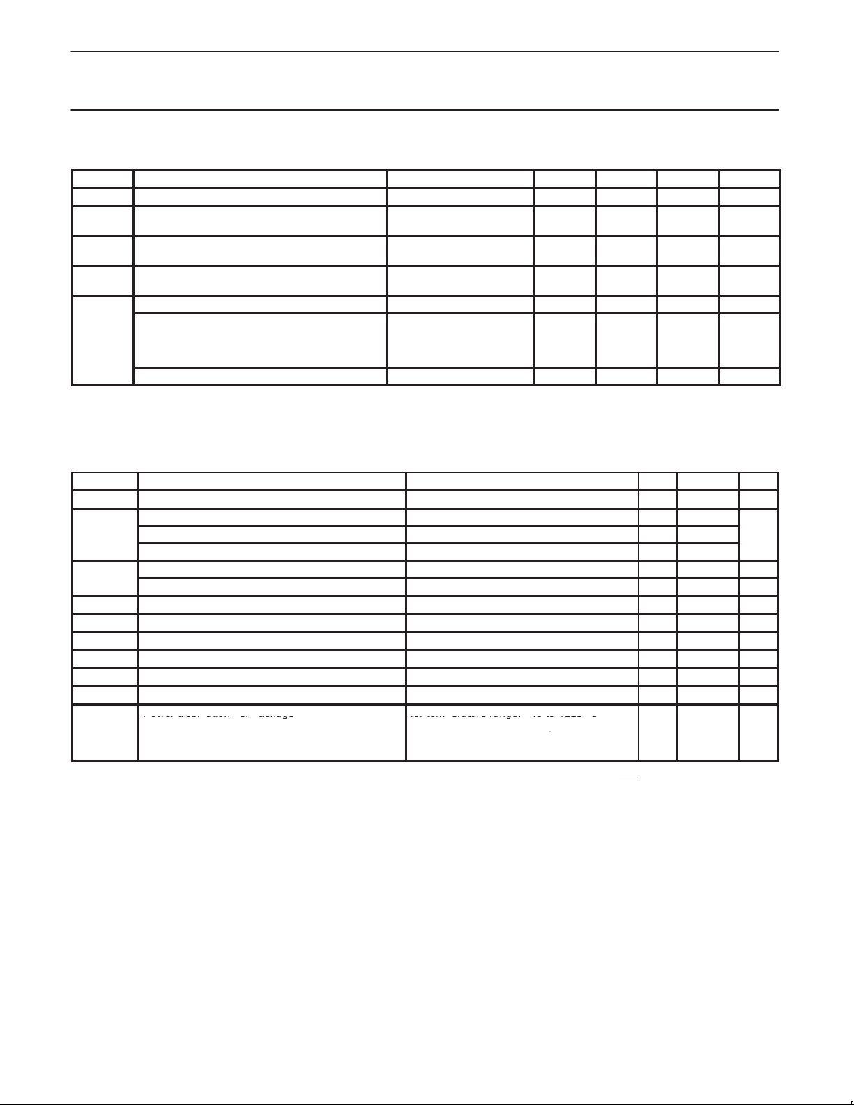
RECOMMENDED OPERATING CONDITIONS
SYMBOL PARAMETER CONDITIONS MIN TYP MAX UNIT
V
V
V
T
amb
tr, t
NOTE:
1. Single sided input protection applied on pins 4, 5, and 9.
DC supply voltage See Note 1 0.9 1.2 6 V
CC
Input voltage pins 4, 5, and 9
I
Input voltage pins 7, 13, 14, and 15
Output voltage pins 10, 11, and 12
O
Output voltage pins 1, 2, 3, and 6
Operating ambient temperature range in free air
See DC and AC
characteristics per device
0
0
0
0
–
–
–
–
0 +70 °C
Input rise and fall times pin 5 – – 10 ms
Input rise and fall times pins 7, 14 and 15
f
VCC = 1.0V; VI = 1.0V
VCC = 2.0V; VI = 2.0V
V
= 3.0V; VI = 4.5V
CC
VCC = 3.6V; VI = 6.0V
–
–
–
–
–
–
–
–
Input rise and fall times pin 9 – – 2 µs
10
V
V
10
500
200
100
50
CC
CC
V
V
ns
ABSOLUTE MAXIMUM RATINGS
2, 3
In accordance with the Absolute Maximum Rating System (IEC 134).
Voltages are referenced to GND (ground = 0 V).
SYMBOL
V
CC
I
IK
I
I
OK
I
O
I
OK
I
O
I
, I
GND
CC
T
stg
DC supply voltage –0.5 +7.0 V
DC input diode current pins 4, 5 and 9 V
DC input diode current pins 7, 13, 14 and 15 V
NON repetitive peak DC input diode current pin 9
DC input voltage range pins 4, 5 and 9 –0.5 +12 V
DC input voltage range pins 7, 13, 14 and 15 –0.5 VCC + 0.5 V
DC output diode current pins 1, 2, 3 and 6 VO < –0.5 V –20 mA
DC output sink current pins 1, 2, 3 and 6 VO > 0 V –25 mA
DC output diode current pins 10, 11 and 12 VO < –0.5 or V
DC output sink or source current pins 10, 11 and 12 –0.5 V < VO < VCC + 0.5 V ±25 mA
DC GND or VCC current ±50 mA
Storage temperature range –65 +150 °C
PARAMETER CONDITIONS MIN MAX UNIT
< –0.5 or VI > 12 V ±20
I
< –0.5 or VI > VCC + 0.5 V +20
I
V
> 10 V and t < 10 s; see note 1
I
> VCC + 0.5 V ±20 mA
O
10
Power dissipation per package for temperature range: –40 to +125 °C
Plastic DIL
tot
Plastic mini-pack (SO)
astic shrink mini-pack
and
above + 70 °C derate linearly with 12 mW/K 750
above + 70 °C derate linearly with 8 mW/K
above + 60 °C derate linearly with 5.5 m
500
400
NOTES:
1. In applications where a motor is present, the input voltage may exceed the maximum V
when the motor is switched off.
, level of 10 V at the DIS input for a very short period
I
2. Stresses beyond those listed may cause permanent damage to the device. These are stress ratings only and functional operation of the
device at these or any other conditions beyond those under “recommended operating conditions” is not implied. Exposure to absolute
maximum rated conditions for extended periods may affect device reliability .
3. The input and output voltage ratings may be exceeded if the input and output current ratings are observed.
mA
1998 Apr 20
7
Page 8
Philips Semiconductors Product specification
g
V
V
g
g
g
g
g
g
nA
Pull-u current in 7
µA
Pull-down current in 5
I
A
74LV4799Timer for NiCd and NiMH chargers
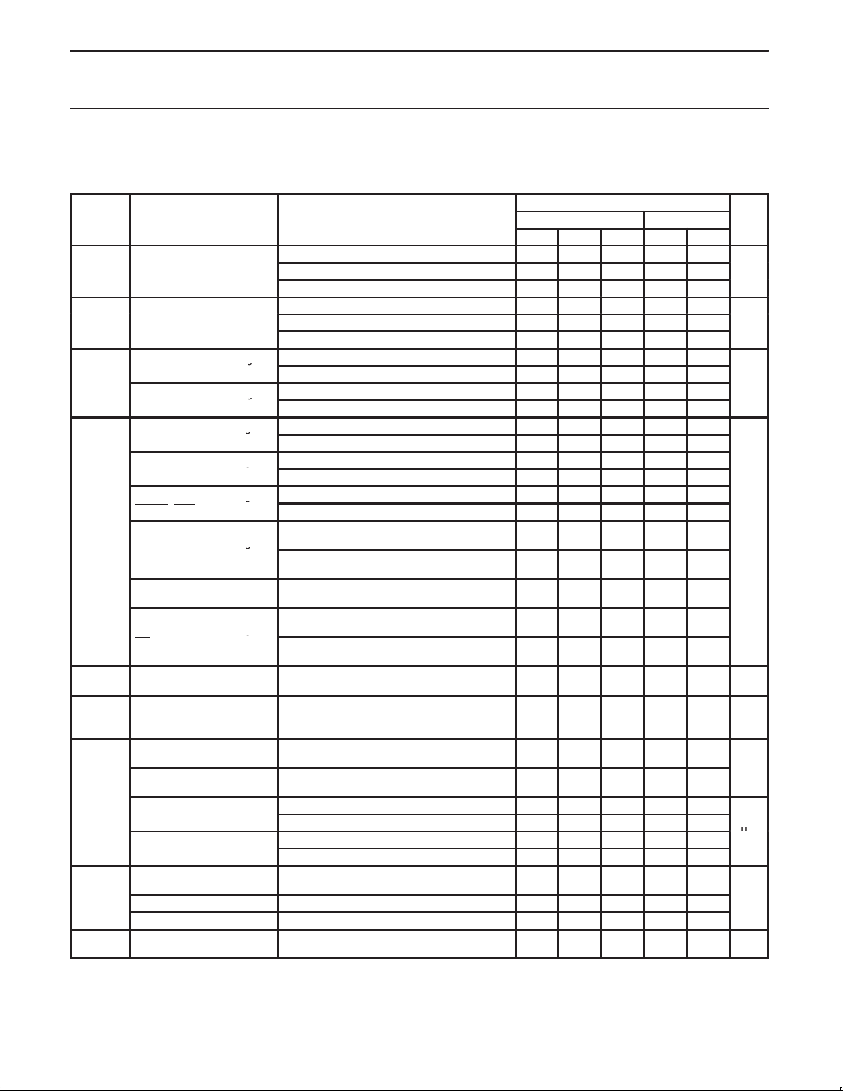
DC ELECTRICAL CHARACTERISTICS
Over recommended operating conditions.
Voltages are referenced to GND (ground = 0 V).
LIMITS
SYMBOL PARAMETER TEST CONDITIONS
VCC = 1.0 V 0.8 0.5 – 0.8 –
V
HIGH level Input voltage
IH
VCC = 4.5 V 3.6 2.4 – 3.6 –
VCC = 6.0 V 4.8 3.2 – 4.8 –
VCC = 1.0 V – 0.5 0.2 – 0.2
V
LOW level Input voltage
IL
VCC = 4.5 V – 2.1 0.9 – 0.9
VCC = 6.0 V – 2.8 1.2 – 1.2
HIGH level output voltage;
RC, RD outputs
OH
HIGH level output voltage;
RS output
LOW level output voltage;
RC, RD outputs
LOW level output voltage;
RS output
LOW level output voltage;
MOLLI, LED outputs
VCC = 1.0 V; VI = VIH or V
VCC = 6.0 V; VI = VIH or V
VCC = 1.0 V; VI = VIH or V
VCC = 6.0 V; VI = VIH or V
VCC = 1.0 V; VI = VIH or V
VCC = 6.0 V; VI = VIH or V
VCC = 1.0 V; VI = VIH or V
VCC = 6.0 V; VI = VIH or V
VCC = 1.0 V; VI = VIH or V
VCC = 6.0 V; VI = VIH or V
VCC = 1.0 V; VI = VIH or V
V
OL
LOW level output voltage;
EN output
pin 4 open
VCC = 6.0 V; VI = VIH or V
pin 4 open
LOW level output voltage;
EN output
VCC = 1.3 V; VI = VIH or V
VCC = 1.0 V; VI = VIH or V
LOW level output voltage;
EN output
pin 4 HIGH
VCC = 6.0 V; VI = VIH or V
pin 4 HIGH
CC
POR level
active inactive
V
IO = –190µA 0.90 0.96 – 0.89 –
IL;
IO = –6.1mA 5.73 5.84 – 5.66 –
IL;
IO =–24µA 0.90 0.96 – 0.89 –
IL;
IO =–760µA 5.73 5.84 – 5.66 –
IL;
IO = 190µA – 0.04 0.10 – 0.11
IL;
IO = 6.1mA – 0.16 0.26 – 0.33
IL;
IO =24µA – 0.04 0.10 – 0.11
IL;
IO =760µA – 0.16 0.26 – 0.33
IL;
IO = 220µA – 0.04 0.10 – 0.11
IL;
IO = 7.4mA – 0.17 0.26 – 0.33
IL;
IO =360µA;
IL;
IO =13.0mA;
IL;
pin 4 = 10 V
IL;
IO =140µA;
IL;
IO =5.0mA;
IL;
1
VCC = 6.0 V; VI = VCC or GND;
I
CC
I
OZH
Quiescent supply current
Input leakage current
pins 4 and 9
Input leakage current
pins 14 and15
I
p
p
p
OFF-state current
pin 1, 3, and 6
OFF-state current pin 2 VCC = 6.0 V; VO = 6 V; Vin = open – – 100 – –
pins 5, 14, and 15 at GND;
pins 7 and 9 at V
CC
2
VCC = 1.0 V; VI = 10 V – – 500 – –
VCC = 6.0 V; VI = VCC or GND – – 100 – –
VCC = 1.0 V; VI = GND –0.5 –2.4 –10 – –
VCC = 6.0 V; VI = GND –0.5 –2.4 –10 – –
VCC = 1.0 V; VI = V
VCC = 6.0 V; VI = V
CC
CC
VCC = 6.0 V; VI = VIH or V IL; VO = 10 V – – 500 – –
OFF-state current pin 3 VCC = 6.0 V; VI = VIH or V IL; VO = 6 V – – 100 – –
OZ
OFF-state current
pins 10, 11, and 12
I
VCC = 6.0 V; VI = VIH or V IL;
VO = VCC or GND
NOTE:
1. This item guarantees that an external bipolar NPN-transistor can be switched off by the EN output.
2. Oscillator disabled. This can be done by I
= HIGH or LOW.
OC
+25°C 0°C to +70°C
MIN TYP MAX MIN MAX
– 0.04 0.10 – 0.11
– 0.17 0.26 – 0.33
– 0.12 0.35 – 0.40
– 0.04 0.10 – 0.11
– 0.17 0.26 – 0.33
0.25
–
–
0.65
–
0.9
–
–
–
–
– 34 50 – 400 µA
0.5 2.4 10 – –
0.5 2.4 10 – –
– – ±100 – – nA
UNIT
V
V
V
V
n
1998 Apr 20
8
Page 9
Philips Semiconductors Product specification
TEST CONDITIONS
∆f
Oscillator frequency s read
yg
%
δ
Duty factor at in 1
See Note 2
%
δ
Duty factor at in 6
See Note 3
%
t
Debounce su ression at in 9
ms
f
qy
kHz
f
qy
Hz
TEST CONDITIONS
k
RC/R
Resistor range
C1
µF
k
k
R
Resistor range
C1
µF
k
F
C1
Ca acitor range
F
74LV4799Timer for NiCd and NiMH chargers
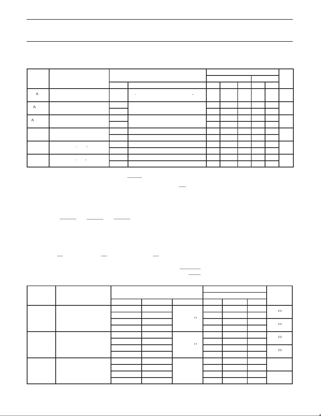
AC CHARACTERISTICS
GND = 0V; tr = tf ≤ 2.5ns; CL = 50pF
T
(°C)
amb
SYMBOL PARAMETER
VCC(V) MIN TYP MAX MIN MAX
1.0
Any resistor or capacitor according to
the application information, see note 1
6.0
1.0
6.0
1.0
6.0
1.0 – 67
6.0 – 65
1.0 100
6.0 100
1.0 50
6.0 50
LED
MOLLI
deb
i(max)
i(min)
p
p
p
pp
p
Maximum frequency at power
sense input
Minimum frequency at power
sense input
NOTES:
1. The oscillator frequency can be calculated by:
2. During blinking.
f
0.36
R C1
3. An output signal of four periods will appear in case of discharged batteries and DIS
is switched HIGH.
+25 0 to +70
–11 –4 +3
–9 –2 +5
– 50
– 50
– 50
– 50
UNIT
APPLICATION INFORMATION
Oscillator.
The frequency will be determined by the external components R
0.36
expressions:
R
and C1 determine the charge time.
C
and C1 determine the discharge time.
R
D
R
and C1 determine the self-charge time.
S
f
R
C1
C
;
f
R
D
0.36
C1
0.36
;
f
R
C1
S
.
The charge, discharge and self-discharge times can be calculated as follows:
Charge time
22
2
;
Discharge time
f
C
18
2
;
Self-discharge time
f
D
In the trickle charge mode, the average charge current will be reduced by a factor:
External components range
SYMBOL PARAMETER
VCC(V) V
1.0 5.360 100
D
2.0
4.5
6.0 0.511 100
1.0 42.20 825
S
2.0
4.5
6.0 3.32 825
1.0 no limit
p
2.0 no limit
4.5 no limit
6.0 no limit
, RD, RS, and C1. The frequencies can be calculated by the following
C
27
2
f
S
1
1
3xR
4xR
S
C
T
(°C)
amb
1
+25
OTHER MIN TYP MAX
= 0.22
= 0.22
1.150 100
0.562 100
9.09 825
4.22 825
UNIT
p
p
1998 Apr 20
9
Page 10
Philips Semiconductors Product specification
C
ithin th
g
given in Section External com onents range
SYMBOL
PARAMETER
CC
UNIT
V
Offset voltage
t
Pro agation delay
R
P-channel resistance R
R
out uts
R
N-channel resistance R
R
out uts
R
P-channel resistance R
out ut
R
N-channel resistance R
out ut
74LV4799Timer for NiCd and NiMH chargers
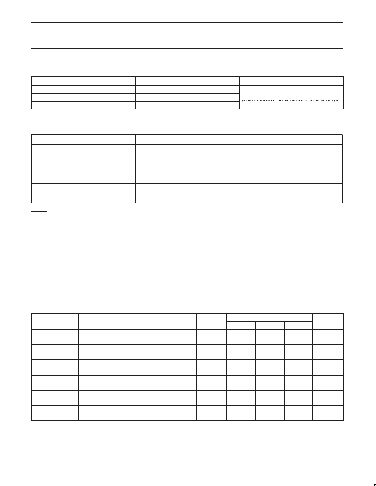
Charge discharge times
PARAMETER
TIME RANGE CONDITIONS
Charge time 4 hours to 16 hours
Discharge time 15 minutes to to 4.7 hours
Self-discharge time 50 days to 100 days
LED frequency
The frequency of the LED
output (pin1) is determined by the oscillator frequency.
Three modes of operation, each with its own frequency, are possible.
Mode SEL LED frequency
Charge
H or open
Trickle charge
Alarm
pulse duration
MOLLI
The MOLLI output gives an output signal of four periods with a 50%
duty cycle. The duration of one period is determined by: 16/f
s
Timing accuracy .
The timing accuracy depends on the accuracy of the on–chip
oscillator and on the external R and C components. The inaccuracy
of the on–chip oscillator is specified as maximum +/–7%. In most
cases the actual inaccuracy will be significantly lower. This depends
on the supply voltage as well as the value of the external
components.
Influence of Resistor value.
Low resistor values cause some spread because the RC
combination is biased by a 3–State push–pull output. The spread of
omponents ranges are w
e values
iven in Section “External components range”
f
C
256
1
8
L
H
the R
of the push–pull stage will contribute to the frequency
on
6
f
f
C
S
f
D
32
spread. When high–value resistors are used, any possible output
leakage of the not–selected 3–State outputs will cause a frequency
deviation. For these reasons, the resistor values must be within the
specified ranges.
Influence of supply voltage
The trip levels of the oscillator are fixed at 20% and 80% of V
higher supply voltages the spread of the trip levels decreases in
greater proportion because the offset voltage remains constant, and
the propagation delay decreases. Furthermore, the R
values of
on
the push–pull driving stage decrease at higher voltages.
. At
cc
SPREAD-CAUSING FACTORS
off
P
ON
ON
ON
ON
1998 Apr 20
p
T
(°C)
V
(V)
MIN TYP MAX
amb
1.0 7 mV
6.0 7 mV
1.0 22
6.0 5.5
p
,
C
D
p
,
C
D
p
S
p
S
1.0 170
6.0 25
1.0 250
6.0 35
1.0 1300
6.0 180
1.0 1300
6.0 180
ms
ms
W
W
W
W
W
W
W
W
10
Page 11
Philips Semiconductors Product specification
74LV4799Timer for NiCd and NiMH chargers
Error free operation, even under extreme conditions.
Several measures are taken in the circuit design to ensure
error–free operation, even with very low supply voltages. Moreover,
the circuit has been made very insensitive to the effects of external
fields. The measures taken during the design are:
•Use of synchronous logic
•Bistable POR instead of monostable POR
•Data retention assured below a supply voltage of 0.9 V .
•Debounce circuitry on DIS input (maximum expected debounce
time = 10 ms)
•Schmitt trigger on PWRS (power sense) input and on DIS input
•Special oscillator security to prevent any malfunction.
Synchronous logic and bistable POR.
Use of synchronous logic results in much lower sensitivity to spikes
on input pins. The POR is adapted to fit well into a synchronous
environment. An increasing supply voltage sets the POR. The POR
output signal is routed to the control logic and divider/counter. it is
synchronized with the on–chip clock. After all flip–flops are reset, a
reset acknowledge signal is generated which resets the POR. This
method ensures that the POR signal is acknowledged in all cases,
even at very low voltages.
Data retention.
The circuit may be used in an application where an electric motor is
present. When the motor is switched on, it will disturb the supply
voltage for a short period. The POR level is set at such a level that,
even with very low supply voltages, the POR will not respond during
motor switch on. The flip–flops will retain their data during the supply
voltage disturbance because of the inherent data retention of any
CMOS gate. However, when the battery is almost completely
discharged and the motor switch is activated, the dip on the supply
voltage line can be too large. The retention of the POR is therefore
made deliberately worse than that of the internal flip–fops. The POR
will therefore respond long before the flip–flops will loose their data.
This results in a proper start condition for a new charge cycle.
Debounce circuitry on DIS
A discharge cycle is activated by a switch. To protect the circuit from
any bounce of the switch contacts, de–bounce circuitry is provided
input.
at the DIS
input. The circuitry allows a switch de–bounce time of
max. 10 ms.
Schmitt trigger on PWRS (power sense) input.
The PWRS input can be corrupted by high transients due to
disturbances on the mains supply. To suppress any false triggering,
the PWRS input is provided with a Schmitt–trigger. However, for
some applications, it is advisable to connect a low–value capacitor
(150 pF min.) between the PWRS input and GND.
Special oscillator security to prevent any malfunction.
The excellent performance of the oscillator is achieved by using
linear op–amp techniques. The oscillator consists of an internal
reference, two comparators and a latch. Care was taken to design a
very reliable oscillator even with a supply voltage below 0.9 V . If one
of the comparators ceases to operate with a supply voltage below
0.9 V , the latch will not be corrupted. Priority was given to stop the
oscillator rather than allow uncontrolled oscillation.
All these measures result in reliable 1-cell to 4-cell battery charge
management.
Remaining energy indication:
The scan test facility can be used as a remaining energy indication
because the value of the counter can be read–out at the scan output
(MOLLI
/SCO). This is achieved by briefly interrupting the normal
mode of operation, putting the circuit in the scan mode
(pin 14 = HIGH), and reading–out of the counter value. The circuit is
then returned to the normal mode (pin 14 = LOW or open).
Read–out procedure: The contents of the counter flip–flops can be
read–out in the scan mode. To ensure that there is no disturbance of
the circuit function, it is essential to either create a round coupled loop
by linking the MOLLI
/SCO output (pin 6) directly to the SCI input
pin 15), or to shift–in the serial data of the scan line at the SCI input
after completion of the read out cycle. 49 clock pulses are needed on
the Iosc input (pin 13) to shift–out the contents of the whole scan line.
The most–significant bit of the counter will appear at the MOLLI
/SCO
output after the last clock pulse. The least–significant bit after the
penultimate clock pulse, etc. Selecting the last three or four bits will
yield sufficiently high accuracy to obtain the counter value which
represents the remaining energy of the battery.
AC
mains
1998 Apr 20
BYD13D BYD13D
220 V
BZD23
110 V
BZD23
BYD13D
BC327/
BC636
n.c.
BYD13D
BC557
43
V
in
1
LED
5
PWRS
7
SEL
14
SCAN
15
SCI
R
74LV4799
RDRSI
C
10 11 12 13 8
OSC
EN
V
MOLLI
DIS
EN
CC
BC547
2
16
6
9
Figure 2. Typical application of the low-voltage 74LV4799.
11
R
Z
BC557
LOAD
battery
buzzer
SV01647
Page 12
Philips Semiconductors Product specification
74LV4799Timer for NiCd and NiMH chargers
33E
100–240 VAC
12/24 VDC
1
V
in
6
VAC2
7
VAC1
8
PWR/LED
9
EN
10
TEA1400
1µF
DRN
VAT
SRC
VIC
GNDC
1.0 mH
2µ2
2µ2
20
16
15
14
13
S2
12
S1
11
1µF
TR1
1E
10µ
TR1
16
V
3
EN
R
5
PWRS
CC
RDRSI
C
10 11 12 13
V
in
74LV4799
OSC
14
LED
DIS
GNDSEL
78
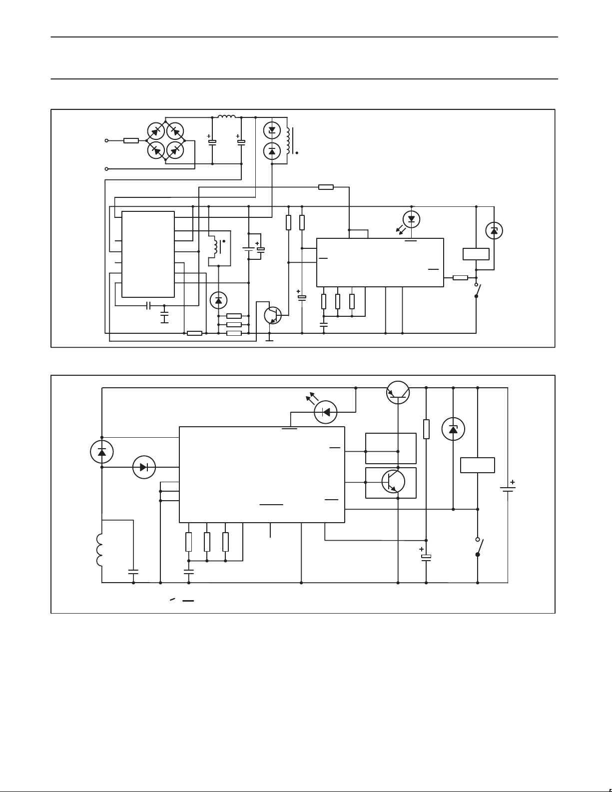
Figure 3. Application diagram of the 74LV4799 in combination with the high-voltage IC TEA1400.
Q1
1
BYD13D
BYD13D
4
V
in
5
PWRS
7
SEL
14
SCAN
15
SCI
R
RDRSI
C
10 11 12 13 8 166
74LV4799
OSC
MOLLI/
SCO
LED
GND
A
3
EN
B
2
EN
DIS
V
CC
Q2
9
R
Z
LOAD
9
S
SV01648
Z
1
LOAD
battery
1998 Apr 20
L
S
Option A: At V
be directly biased by EN
CC
> 2.0 V Q1 may
Option B: At V
an extra NPN transistor (Q2)
< 2.0 V add
CC
Figure 4. Inductive loader, showing the two options A and B.
12
SV01649
Page 13
Philips Semiconductors Product specification
Timer for NiCd and NiMH chargers
DIP16: plastic dual in-line package; 16 leads (300 mil) SOT38-4
74LV4799
1998 Apr 20
13
Page 14
Philips Semiconductors Product specification
Timer for NiCd and NiMH chargers
SO16: plastic small outline package; 16 leads; body width 3.9 mm SOT109-1
74LV4799
1998 Apr 20
14
Page 15
Philips Semiconductors Product specification
Timer for NiCd and NiMH chargers
SSOP16: plastic shrink small outline package; 16 leads; body width 5.3 mm SOT338-1
74LV4799
1998 Apr 20
15
Page 16
Philips Semiconductors Product specification
Timer for NiCd and NiMH chargers
TSSOP16: plastic thin shrink small outline package; 16 leads; body width 4.4 mm SOT403-1
74LV4799
1998 Apr 20
16
Page 17

Philips Semiconductors Product specification
Timer for NiCd and NiMH chargers
74LV4799
NOTES
1998 Apr 20
17
Page 18

Philips Semiconductors Product specification
74LV4799Timer for NiCd and NiMH chargers
Data sheet status
Data sheet
status
Objective
specification
Preliminary
specification
Product
specification
Product
status
Development
Qualification
Production
Definition
This data sheet contains the design target or goal specifications for product development.
Specification may change in any manner without notice.
This data sheet contains preliminary data, and supplementary data will be published at a later date.
Philips Semiconductors reserves the right to make chages at any time without notice in order to
improve design and supply the best possible product.
This data sheet contains final specifications. Philips Semiconductors reserves the right to make
changes at any time without notice in order to improve design and supply the best possible product.
[1]
[1] Please consult the most recently issued datasheet before initiating or completing a design.
Definitions
Short-form specification — The data in a short-form specification is extracted from a full data sheet with the same type number and title. For
detailed information see the relevant data sheet or data handbook.
Limiting values definition — Limiting values given are in accordance with the Absolute Maximum Rating System (IEC 134). Stress above one
or more of the limiting values may cause permanent damage to the device. These are stress ratings only and operation of the device at these or
at any other conditions above those given in the Characteristics sections of the specification is not implied. Exposure to limiting values for extended
periods may affect device reliability.
Application information — Applications that are described herein for any of these products are for illustrative purposes only. Philips
Semiconductors make no representation or warranty that such applications will be suitable for the specified use without further testing or
modification.
Disclaimers
Life support — These products are not designed for use in life support appliances, devices or systems where malfunction of these products can
reasonably be expected to result in personal injury . Philips Semiconductors customers using or selling these products for use in such applications
do so at their own risk and agree to fully indemnify Philips Semiconductors for any damages resulting from such application.
Right to make changes — Philips Semiconductors reserves the right to make changes, without notice, in the products, including circuits, standard
cells, and/or software, described or contained herein in order to improve design and/or performance. Philips Semiconductors assumes no
responsibility or liability for the use of any of these products, conveys no license or title under any patent, copyright, or mask work right to these
products, and makes no representations or warranties that these products are free from patent, copyright, or mask work right infringement, unless
otherwise specified.
Philips Semiconductors
811 East Arques Avenue
P.O. Box 3409
Sunnyvale, California 94088–3409
Telephone 800-234-7381
Copyright Philips Electronics North America Corporation 1998
All rights reserved. Printed in U.S.A.
print code Date of release: 05-96
Document order number: 9397-750-04664
yyyy mmm dd
18
 Loading...