

Page 1
Low-voltage CMOS hex buffer (open drain)
Features
■ 5 V tolerant inputs
■ High speed
–t
= 5.2 ns (max) at V
PD
■ Power-down protection on inputs and outputs
■ Symmetrical output impedance
–|I
■ PCI bus levels guaranteed at 24 mA
■ Operating voltage range
–V
■ Pin and function compatible with 74 series 07
■ Latch-up performance exceeds 500 mA
| = IOL = 24 mA (min) at VCC = 3 V
OH
(opr) = 2.0 V to 3.6 V
CC
(JESD 17)
■ ESD performance
– HBM > 2000V
(MIL STD 883 method 3015); MM > 200V
Applications
■ Automotive
■ Industrial
■ Computer
■ Consumer
CC
= 3 V
74LCX07
with 5 V tolerant inputs
Datasheet − production data
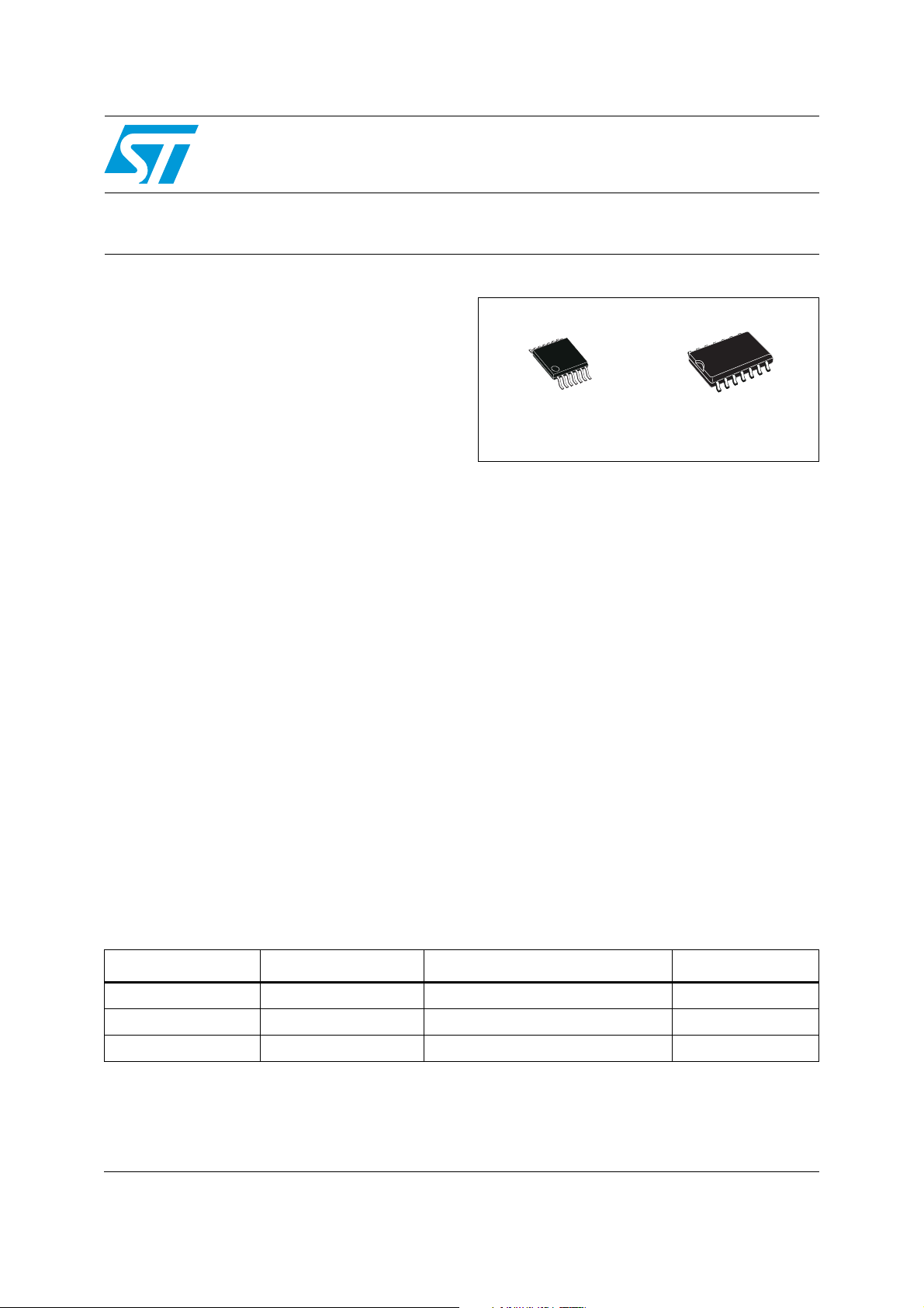
TSSOP14
Description
The 74LCX07 is a low-voltage CMOS open drain
hex buffer manufactured with sub-micron silicon
gate and double-layer metal wiring C
technology. It is ideal for low-power and highspeed 3.3 V applications and can be interfaced to
a 5 V signal environment for inputs.
The internal circuit is composed of 2 stages
including a buffer output, which provides high
noise immunity and stable output.
It has the same speed performance at 3.3 V as
the 5 V AC/ACT family, combined with lower
power consumption.
All inputs and outputs are equipped with
protection circuits against static discharge, giving
them 2 kV ESD immunity and transient excess
voltage.
SO-14
2
MOS
Table 1. Device summary
Part number Temperature range Package Packaging
74LCX07TTR -40/+85 °C TSSOP14 Tape and reel
74LCX07YTTR
74LCX07MTR -40/+85 °C SO-14 Tape and reel
1. Qualification and characterization (according to AEC Q100 and Q003 or equivalent) and advanced screening (according to
AEC Q001 and Q002 or equivalent) are ongoing.
June 2012 Doc ID 6818 Rev 7 1/16
This is information on a product in full production.
(1)
-40/+125 °C TSSOP14 (automotive grade) Tape and reel
www.st.com
16
Page 2

Contents 74LCX07
Contents
1 Logic symbols and I/O equivalent circuit . . . . . . . . . . . . . . . . . . . . . . . . 3
2 Pin settings . . . . . . . . . . . . . . . . . . . . . . . . . . . . . . . . . . . . . . . . . . . . . . . . 4
2.1 Pin connections . . . . . . . . . . . . . . . . . . . . . . . . . . . . . . . . . . . . . . . . . . . . . 4
2.2 Pin description . . . . . . . . . . . . . . . . . . . . . . . . . . . . . . . . . . . . . . . . . . . . . . 4
2.3 Truth table . . . . . . . . . . . . . . . . . . . . . . . . . . . . . . . . . . . . . . . . . . . . . . . . . . 4
3 Maximum ratings . . . . . . . . . . . . . . . . . . . . . . . . . . . . . . . . . . . . . . . . . . . . 5
3.1 Recommended operating conditions . . . . . . . . . . . . . . . . . . . . . . . . . . . . . 5
4 Electrical characteristics . . . . . . . . . . . . . . . . . . . . . . . . . . . . . . . . . . . . . 6
5 Test circuit . . . . . . . . . . . . . . . . . . . . . . . . . . . . . . . . . . . . . . . . . . . . . . . . . 8
6 Waveforms . . . . . . . . . . . . . . . . . . . . . . . . . . . . . . . . . . . . . . . . . . . . . . . . . 9
7 Package mechanical data . . . . . . . . . . . . . . . . . . . . . . . . . . . . . . . . . . . . 10
8 Revision history . . . . . . . . . . . . . . . . . . . . . . . . . . . . . . . . . . . . . . . . . . . 15
2/16 Doc ID 6818 Rev 7
Page 3
74LCX07 Logic symbols and I/O equivalent circuit
1 Logic symbols and I/O equivalent circuit
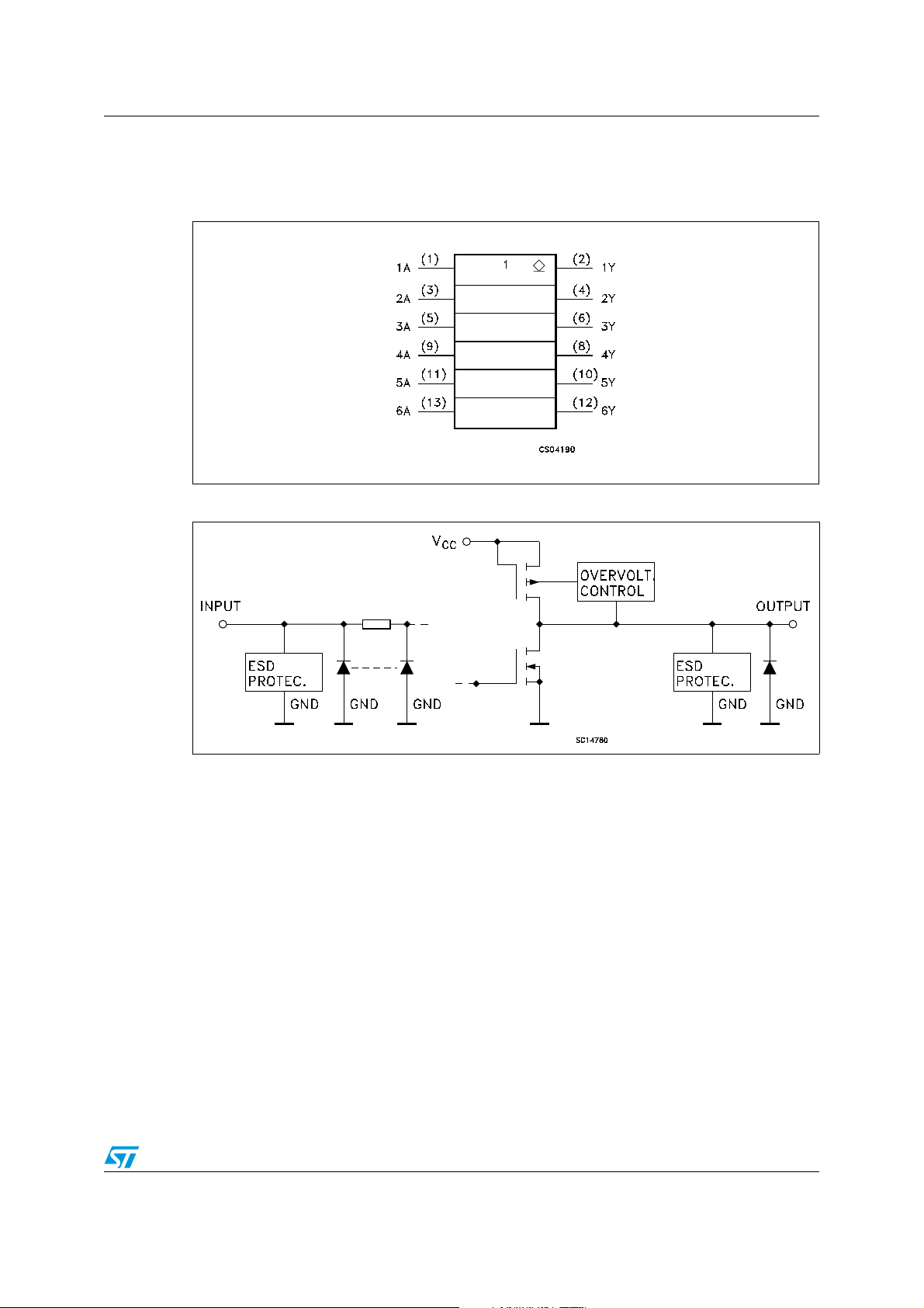
Figure 1. IEC logic symbols
Figure 2. Input and output equivalent circuit
Doc ID 6818 Rev 7 3/16
Page 4
Pin settings 74LCX07
2 Pin settings
2.1 Pin connections
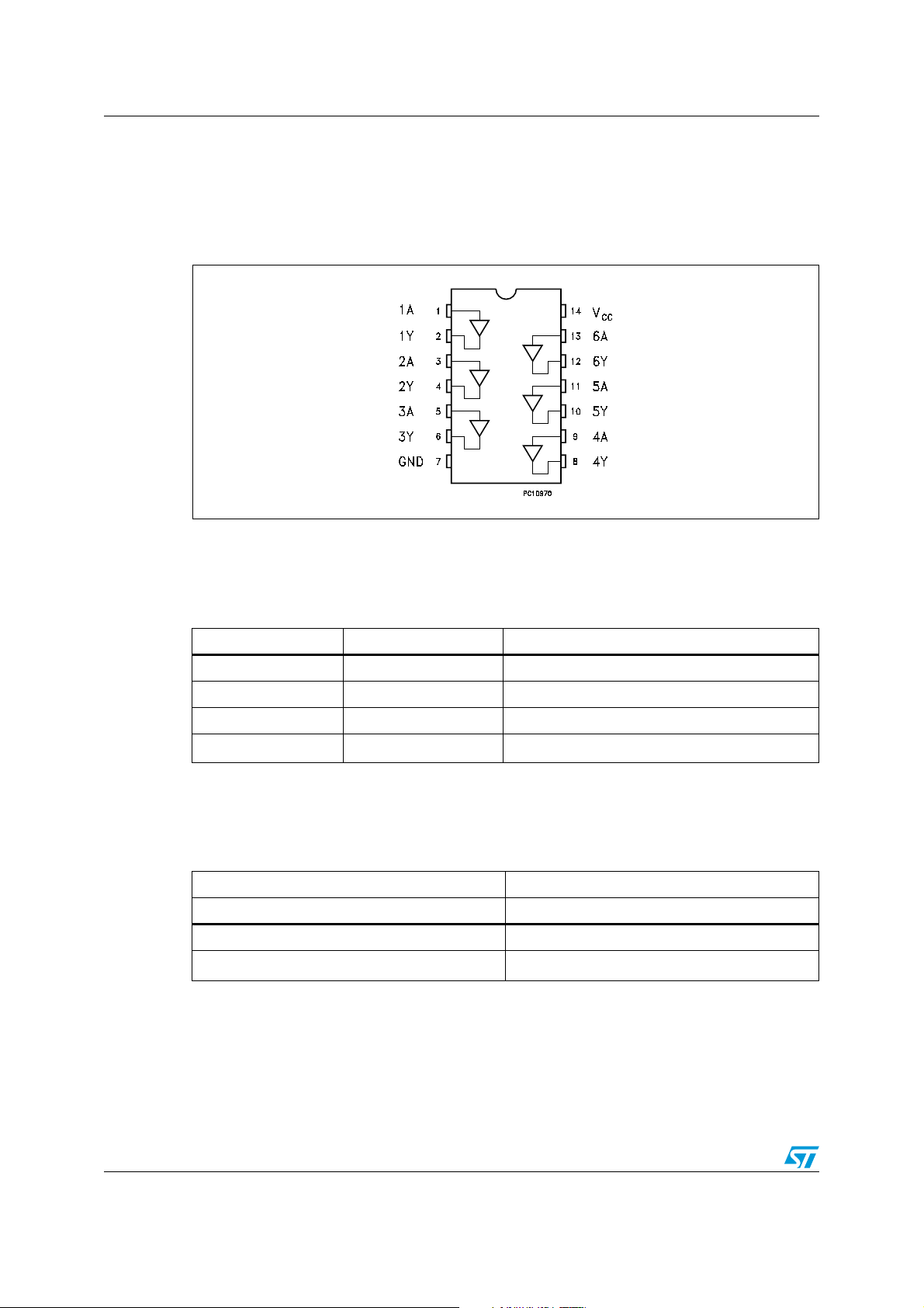
Figure 3. Pin connections (top through view)
2.2 Pin description
Table 2. Pin description
Pin number Symbol Name and function
1, 3, 5, 9, 11, 13 1A to 6A Data inputs
2, 4, 6, 8, 10, 12 1Y to 6Y Data outputs
7 GND Ground (0 V)
14 V
2.3 Truth table
Table 3. Truth table
Input Output
1. High impedance
CC
AY
LL
H
Positive supply voltage
Z
(1)
4/16 Doc ID 6818 Rev 7
Page 5
74LCX07 Maximum ratings
3 Maximum ratings
Stressing the device above the rating listed in the “absolute maximum ratings” table may
cause permanent damage to the device. These are stress ratings only and operation of the
device at these or any other conditions above those indicated in the operating sections of
this specification is not implied. Exposure to absolute maximum rating conditions for
extended periods may affect device reliability.
Table 4. Absolute maximum ratings
Symbol Parameter Value Unit
V
I
I
I
GND
T
1. IO absolute maximum rating must be observed
2. VO < GND
Supply voltage -0.5 to +7.0 V
CC
DC input voltage -0.5 to +7.0 V
V
I
V
DC output voltage (VCC = 0 V) -0.5 to +7.0 V
O
V
DC output voltage (high or low state)
O
I
DC input diode current -50 mA
IK
DC output diode current
OK
I
DC output current ± 50 mA
O
DC supply current per supply pin ± 100 mA
CC
(2)
(1)
DC ground current per supply pin ± 100 mA
Storage temperature -65 to +150 °C
stg
Lead temperature (10 sec) 300 °C
T
L
3.1 Recommended operating conditions
Table 5. Recommended operating conditions
Symbol Parameter Value Unit
Supply voltage
CC
Input voltage 0 to 5.5 V
I
Output voltage (VCC = 0 V) 0 to 5.5 V
O
Output voltage (high or low state) 0 to V
O
, IOLHigh or low level output current (VCC = 3.0 to 3.6 V) ± 24 mA
, IOLHigh or low level output current (VCC = 2.7 V) ± 12 mA
Operating temperature
op
I
I
V
V
V
V
OH
OH
T
dt/dv Input rise and fall time
(1)
TSSOP14, SO-14 -40 to +85 °C
TSSOP14 (automotive grade) -40 to +125 °C
(2)
-0.5 to VCC + 0.5
-50 mA
2.0 to 3.6 V
0 to 10 ns/V
CC
V
V
1. Truth table guaranteed: 1.5 V to 3.6 V
2. VIN from 0.8 V to 2 V at VCC = 3.0 V
Doc ID 6818 Rev 7 5/16
Page 6
Electrical characteristics 74LCX07
4 Electrical characteristics
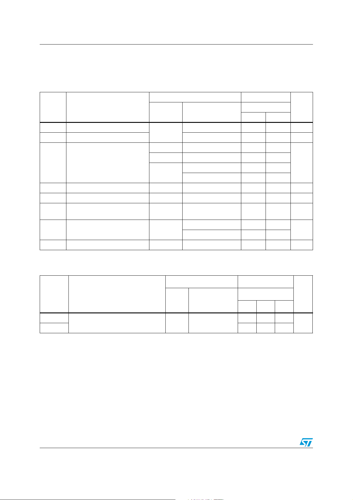
Table 6. DC specifications
Test condition Value
Symbol Parameter
V
V
V
I
I
I
ΔI
High level input voltage
IH
Low level input voltage 0.8 V
IL
Low level output voltage
OL
Input leakage current 2.7 to 3.6 VI = 0 to 5.5 V ± 5 μA
I
I
Power OFF leakage current 0 VI or VO = 5.5 V 10 μA
off
High impedance output leakage
OZ
current
Quiescent supply current 2.7 to 3.6
CC
I incr. per input 2.7 to 3.6 VIH = VCC - 0.6 V 500 μA
CC
V
CC
(V)
2.7 to 3.6
2.7 to 3.6 I
2.7 I
3.0
2.7 to 3.6
VI = VCC or GND 10
or VO = 3.6 to 5.5 V ± 10
V
I
-40 to 85 °C
Min Max
2.0 V
= 100 μA0.2
O
= 12 mA 0.4
O
I
= 16 mA 0.4
O
I
= 24 mA 0.55
O
VI = VIH or V
VO = 0 to V
CC
IL
± 5 μA
Unit
V
μA
Table 7. Dynamic switching characteristics
Test condition Value
Symbol Parameter
V
CC
(V)
V
OLP
V
OLV
1. Number of outputs defined as "n". Measured with "n-1" outputs switching from HIGH to LOW or LOW to HIGH. The
remaining output is measured in the LOW state.
Dynamic low level quiet output
(1)
3.3
V
IL
V
IH
= 0 V
= 3.3 V
= 25 °C
T
A
Min Typ Max
0.8
-0.8
Unit
V
6/16 Doc ID 6818 Rev 7
Page 7
74LCX07 Electrical characteristics
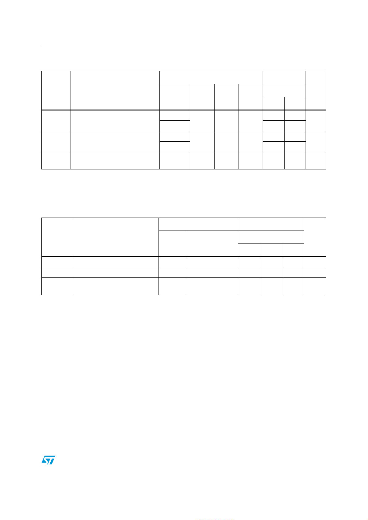
Table 8. AC electrical characteristics
Test condition Value
Symbol Parameter
V
CC
(V)
C
(pF)
L
R
(Ω)
ts = t
L
(ns)
2.7
t
PLZ
Propagation delay time
3.0 to 3.6 1.0 5.2
50 500 2.5
2.7
t
PZL
t
OSLH
t
OSHL
1. Skew is defined as the absolute value of the difference between the actual propagation delay for any two outputs of the
same device switching in the same direction, either HIGH or LOW (t
2. Parameter guaranteed by design
Propagation delay time
Output to output skew time
(1) (2)
3.0 to 3.6 1.0 5.2
50 500 2.5
3.0 to 3.6 50 500 2.5 1.0 ns
OSLH
= | t
PLHm
- t
PLHn
|, t
OSHL
-40 to 85 °C
r
Min Max
= | t
PHLm
- t
7.0
7.0
PHLn
|)
Table 9. Capacitive characteristics
Test condition Value
Symbol Parameter
C
C
OUT
C
PD
1. CPD is defined as the value of the IC’s internal equivalent capacitance which is calculated from the operating current
consumption without load. (Refer to Test Circuit). Average operating current can be obtained by the following equation.
I
CC(opr)
Input capacitance 3.3 VIN = 0 to V
IN
Output capacitance 3.3 VIN = 0 to V
Power dissipation capacitance
= CPD x VCC x fIN + ICC/6 (per gate)
(1)
V
CC
(V)
3.3
= 10 MHz
f
IN
VIN = 0 or V
Min Typ Max
CC
CC
CC
= 25 °C
T
A
6pF
14 pF
4.3 pF
Unit
ns
ns
Unit
Doc ID 6818 Rev 7 7/16
Page 8
Test circuit 74LCX07
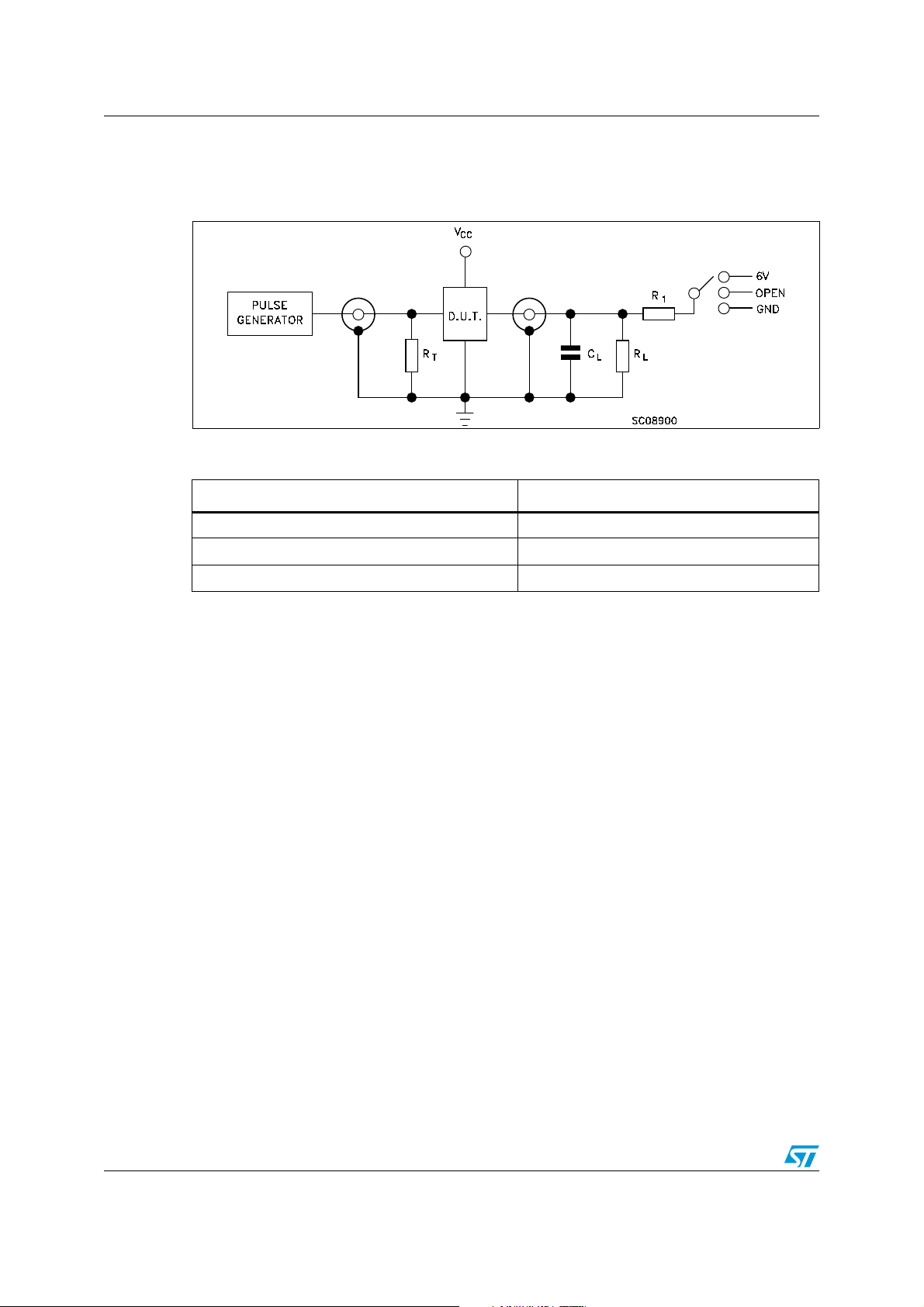
5 Test circuit
Figure 4. Test circuit
Table 10. Test circuit
Tes t Sw itch
, t
t
PLH
PHL
t
, t
PZL
PLZ
, t
t
PZH
PHZ
= 50 pF or equivalent (includes jig and probe capacitance)
C
L
R
= 500 Ω or equivalent
L
R
= Z
T
of pulse generator (typically 50 Ω)
OUT
Open
6 V
GND
8/16 Doc ID 6818 Rev 7
Page 9
74LCX07 Waveforms
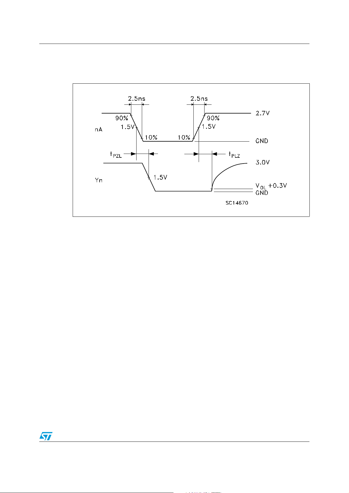
6 Waveforms
Figure 5. Waveform - propagation delay (f = 1 MHz; 50% duty cycle)
Doc ID 6818 Rev 7 9/16
Page 10

Package mechanical data 74LCX07
7 Package mechanical data
In order to meet environmental requirements, ST offers these devices in different grades of
ECOPACK
specifications, grade definitions and product status are available at: www.st.com.
ECOPACK
®
packages, depending on their level of environmental compliance. ECOPACK®
®
is an ST trademark.
10/16 Doc ID 6818 Rev 7
Page 11
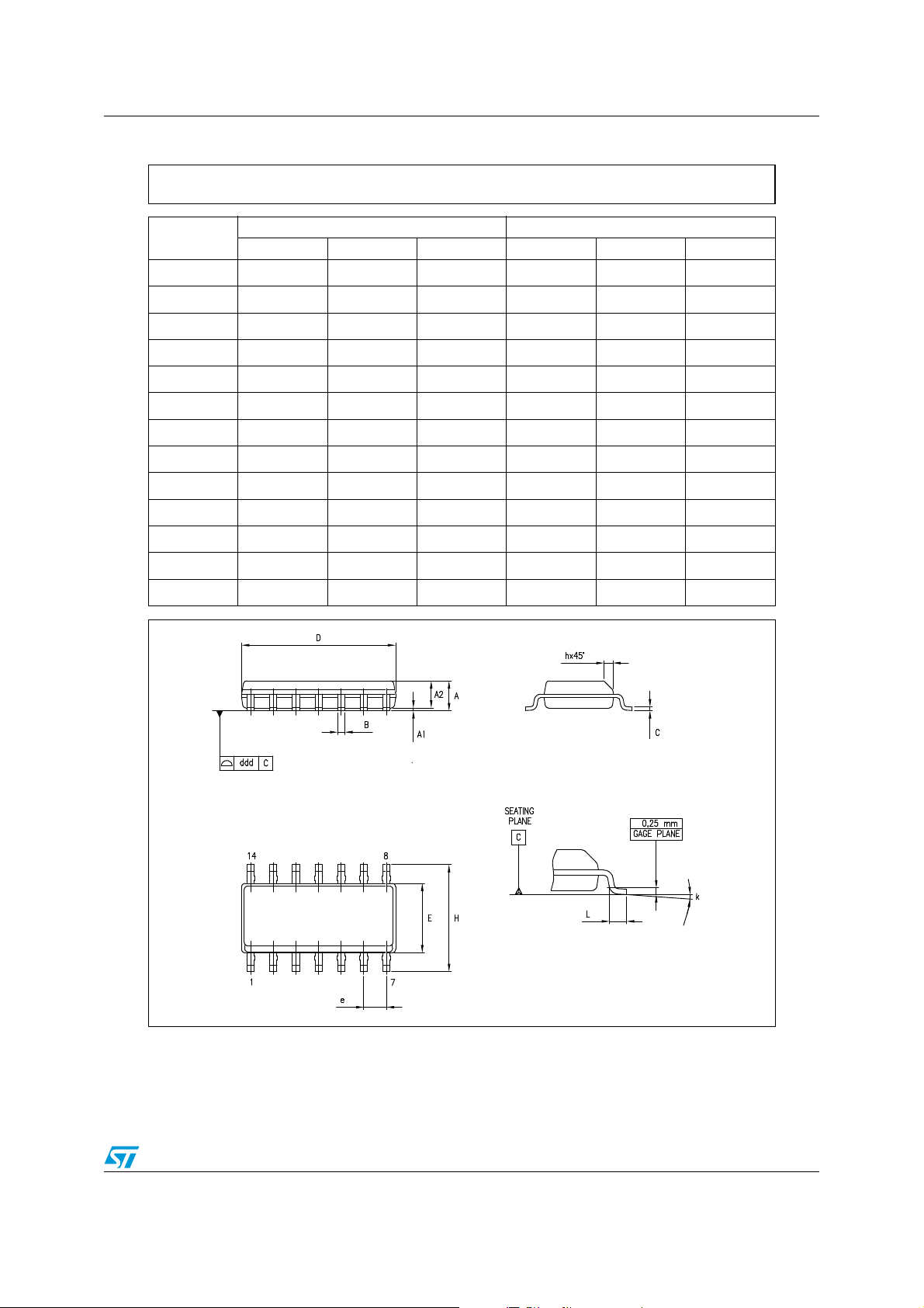
74LCX07 Package mechanical data
SO-14 MECHANICAL DATA
DIM.
A 1.35 1.75 0.053 0.069
A1 0.1 0.25 0.004 0.010
A2 1.10 1.65 0.043 0.065
B 0.33 0.51 0.013 0.020
C 0.19 0.25 0.007 0.010
D 8.55 8.75 0.337 0.344
E 3.8 4.0 0.150 0.157
e 1.27 0.050
H 5.8 6.2 0.228 0.244
h 0.25 0.50 0.010 0.020
L 0.4 1.27 0.016 0.050
k0° 8°0° 8°
ddd 0.100 0.004
MIN. TYP MAX. MIN. TYP. MAX.
mm. inch
0016019D
Doc ID 6818 Rev 7 11/16
Page 12
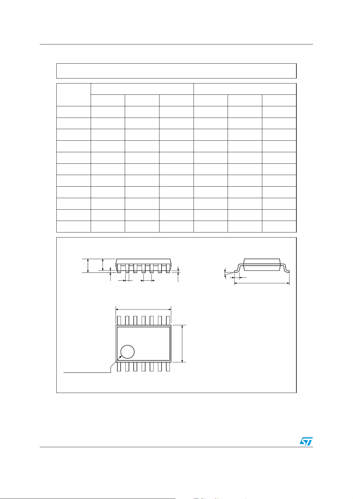
Package mechanical data 74LCX07
TSSOP14 MECHANICAL DATA
DIM.
MIN. TYP MAX. MIN. TYP. MAX.
A 1.2 0.047
A1 0.05 0.15 0.002 0.004 0.006
A2 0.8 1 1.05 0.031 0.039 0.041
b 0.19 0.30 0.007 0.012
c 0.09 0.20 0.004 0.0089
D 4.9 5 5.1 0.193 0.197 0.201
E 6.2 6.4 6.6 0.244 0.252 0.260
E1 4.3 4.4 4.48 0.169 0.173 0.176
e 0.65 BSC 0.0256 BSC
K0˚ 8˚0˚ 8˚
L 0.45 0.60 0.75 0.018 0.024 0.030
mm. inch
A2
A
PIN 1 IDENTIFICATION
A1
b
e
c
K
L
E
D
E1
1
0080337D
12/16 Doc ID 6818 Rev 7
Page 13
74LCX07 Package mechanical data
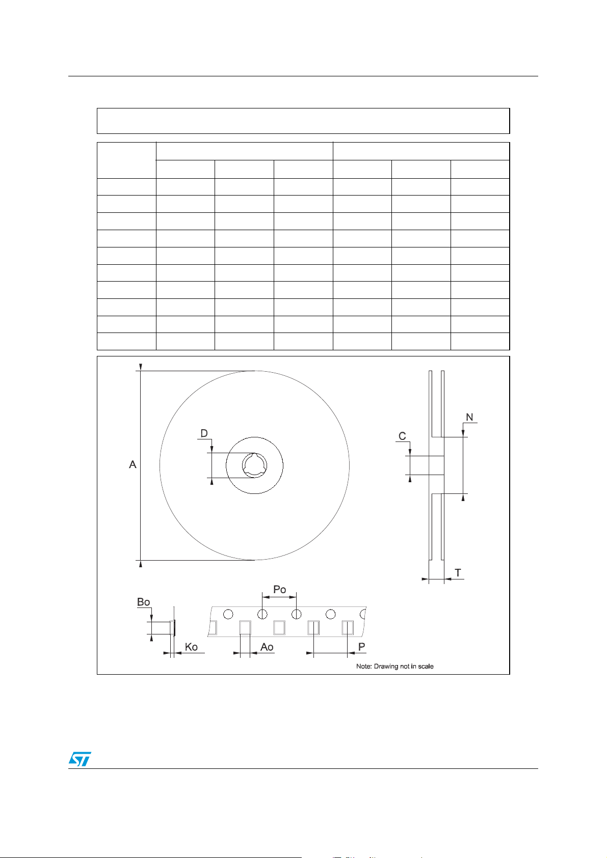
Tape & Reel SO-14 MECHANICAL DATA
DIM.
MIN. TYP MAX. MIN. TYP. MAX.
A 330 12.992
C 12.8 13.2 0.504 0.519
D 20.2 0.795
N 60 2.362
T 22.4 0.882
Ao 6.4 6.6 0.252 0.260
Bo 9 9.2 0.354 0.362
Ko 2.1 2.3 0.082 0.090
Po 3.9 4.1 0.153 0.161
P 7.9 8.1 0.311 0.319
mm. inch
Doc ID 6818 Rev 7 13/16
Page 14
Package mechanical data 74LCX07
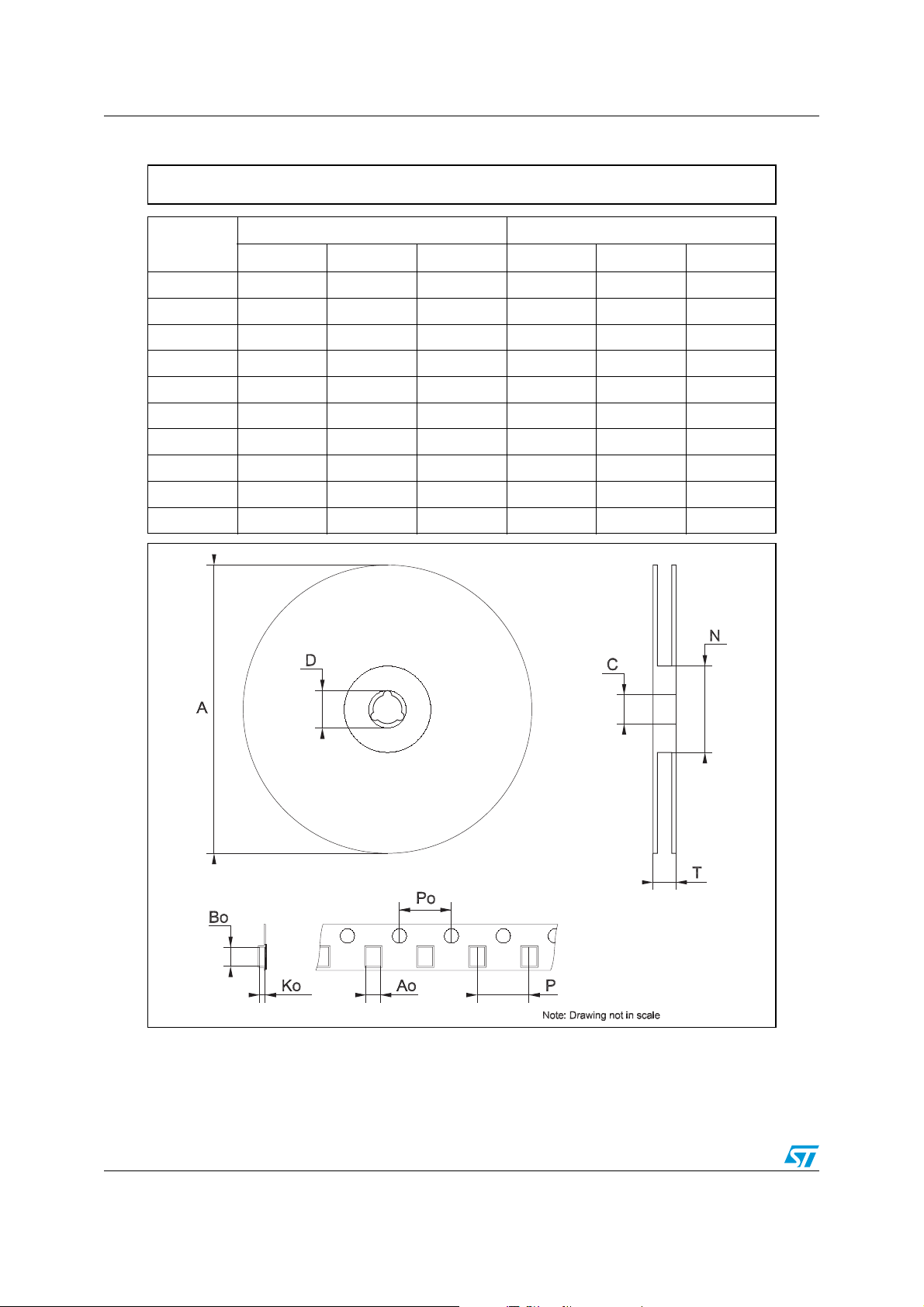
Tape & Reel TSSOP14 MECHANICAL DATA
DIM.
MIN. TYP MAX. MIN. TYP. MAX.
A 330 12.992
C 12.8 13.2 0.504 0.519
D 20.2 0.795
N 60 2.362
T 22.4 0.882
Ao 6.7 6.9 0.264 0.272
Bo 5.3 5.5 0.209 0.217
Ko 1.6 1.8 0.063 0.071
Po 3.9 4.1 0.153 0.161
P 7.9 8.1 0.311 0.319
mm. inch
14/16 Doc ID 6818 Rev 7
Page 15
74LCX07 Revision history
8 Revision history
Table 11. Revision history
Date Revision Changes
15-Sep-2004 4 Ordering codes revision - pag. 1.
10-Jul-2006 5 New template, temperature ranges updated
Added Applications on page 1
Updated Table 1: Device summary on page 1
20-Jun-2012 6
21-Jun-2012 7 Updated Table 1: Device summary
Updated T
Updated ECOPACK® text in Section 7: Package mechanical data
Minor textual updates
in Table 5: Recommended operating conditions
op
Doc ID 6818 Rev 7 15/16
Page 16

74LCX07
Please Read Carefully:
Information in this document is provided solely in connection with ST products. STMicroelectronics NV and its subsidiaries (“ST”) reserve the
right to make changes, corrections, modifications or improvements, to this document, and the products and services described herein at any
time, without notice.
All ST products are sold pursuant to ST’s terms and conditions of sale.
Purchasers are solely responsible for the choice, selection and use of the ST products and services described herein, and ST assumes no
liability whatsoever relating to the choice, selection or use of the ST products and services described herein.
No license, express or implied, by estoppel or otherwise, to any intellectual property rights is granted under this document. If any part of this
document refers to any third party products or services it shall not be deemed a license grant by ST for the use of such third party products
or services, or any intellectual property contained therein or considered as a warranty covering the use in any manner whatsoever of such
third party products or services or any intellectual property contained therein.
UNLESS OTHERWISE SET FORTH IN ST’S TERMS AND CONDITIONS OF SALE ST DISCLAIMS ANY EXPRESS OR IMPLIED
WARRANTY WITH RESPECT TO THE USE AND/OR SALE OF ST PRODUCTS INCLUDING WITHOUT LIMITATION IMPLIED
WARRANTIES OF MERCHANTABILITY, FITNESS FOR A PARTICULAR PURPOSE (AND THEIR EQUIVALENTS UNDER THE LAWS
OF ANY JURISDICTION), OR INFRINGEMENT OF ANY PATENT, COPYRIGHT OR OTHER INTELLECTUAL PROPERTY RIGHT.
UNLESS EXPRESSLY APPROVED IN WRITING BY TWO AUTHORIZED ST REPRESENTATIVES, ST PRODUCTS ARE NOT
RECOMMENDED, AUTHORIZED OR WARRANTED FOR USE IN MILITARY, AIR CRAFT, SPACE, LIFE SAVING, OR LIFE SUSTAINING
APPLICATIONS, NOR IN PRODUCTS OR SYSTEMS WHERE FAILURE OR MALFUNCTION MAY RESULT IN PERSONAL INJURY,
DEATH, OR SEVERE PROPERTY OR ENVIRONMENTAL DAMAGE. ST PRODUCTS WHICH ARE NOT SPECIFIED AS "AUTOMOTIVE
GRADE" MAY ONLY BE USED IN AUTOMOTIVE APPLICATIONS AT USER’S OWN RISK.
Resale of ST products with provisions different from the statements and/or technical features set forth in this document shall immediately void
any warranty granted by ST for the ST product or service described herein and shall not create or extend in any manner whatsoever, any
liability of ST.
ST and the ST logo are trademarks or registered trademarks of ST in various countries.
Information in this document supersedes and replaces all information previously supplied.
The ST logo is a registered trademark of STMicroelectronics. All other names are the property of their respective owners.
© 2012 STMicroelectronics - All rights reserved
STMicroelectronics group of companies
Australia - Belgium - Brazil - Canada - China - Czech Republic - Finland - France - Germany - Hong Kong - India - Israel - Italy - Japan -
Malaysia - Malta - Morocco - Philippines - Singapore - Spain - Sweden - Switzerland - United Kingdom - United States of America
www.st.com
16/16 Doc ID 6818 Rev 7
 Loading...