

Page 1

INTEGRATED CIRCUITS
DATA SH EET
For a complete data sheet, please also download:
•The IC06 74HC/HCT/HCU/HCMOS Logic Family Specifications
•The IC06 74HC/HCT/HCU/HCMOS Logic Package Information
•The IC06 74HC/HCT/HCU/HCMOS Logic Package Outlines
74HC/HCT7731
Quad 64-bit static shift register
Product specification
File under Integrated Circuits, IC06
September 1993
Page 2
Philips Semiconductors Product specification
Quad 64-bit static shift register 74HC/HCT7731
FEATURES
• Frequency range DC to 100 MHz.
• Separate serial data inputs
• Cascadable
• Functionally compatible with
HEF 4731
• Includes recycling mode
• Direct shift out
• Output capability: Standard
• ICC category: LSI.
APPLICATIONS
• Data storage
• Delay line.
GENERAL DESCRIPTION
The HC/HCT7731 are high-speed
Si-gate CMOS devices. They are
specified in compliance with JEDEC
standard no. 7A.
The HC/HCT7731 are quad 64-bit
static shift registers with a recycling
mode. Each register has separate
data inputs D
to Dd, clock inputs CP
a
to CPd and data outputs Qa to Qd.
Data shifts one place towards the
output, each LOW to HIGH transition
of the clock pulse. Each recycling
mode input controls two registers
RECab for registers A and B and
RECcd for registers C and D. When
the REC input is HIGH, the device is
in the recycling mode and data at the
output is shifted back into the input of
the register, so after 64 clock pulses
the contents of a register is again in
its original position. This enables the
user to tap off data from any position.
When the REC input is LOW external
data can be shifted in.
QUICK REFERENCE DATA
GND = 0 V; T
= 25 °C; tr = tf = 6 ns.
amb
TYP.
SYMBOL PARAMETER CONDITIONS
HC HCT
t
PHL/tPLH
f
max
propagation delay
CP
to Q
a-d
a-d
maximum clock
CL = 15 pF;
VCC = 5 V
15 20 ns
100 100 MHz
frequency
C
I
C
PD
input capacitance 3.5 3.5 pF
power dissipation
capacitance per register
notes 1, 2
and 3
58 61 pF
Notes
1. C
is used to determine the dynamic power dissipation (PD in µW):
PD
PD = (CPD x V
2
x fi) + (CL + V
CC
CC
2
x fo) + (I
pull-up
x VCC)
where:
fi = input frequency in MHz.
fo = output frequency in MHz.
VCC = supply voltage in V.
CL = output load capacitance in pF.
I
= pull-up currents in µA.
pull-up
2. For HC the condition is VI = GND to V
CC
For HCT the condition is VI = GND to VCC− 1.5 V.
3. See also power dissipation information.
a
ORDERING INFORMATION
EXTENDED TYPE
NUMBER
PINS PIN POSITION MATERIAL CODE
PACKAGE
74HC/HCT7731N 16 DIL plastic SOT38Z
74HC/HCT7731D 16 SO16 plastic SOT109A
UNIT
September 1993 2
Page 3
Philips Semiconductors Product specification
Quad 64-bit static shift register 74HC/HCT7731
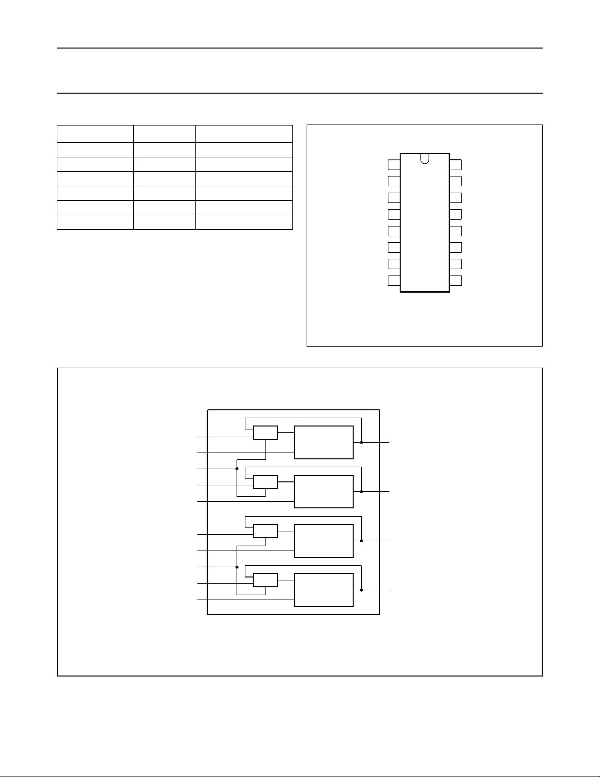
PINNING
SYMBOL PIN DESCRIPTION
Q
to Q
a
d
CP
to CP
D
to D
a
REC
a
, REC
ab
d
d
cd
GND 8 ground (0 V)
V
CC
1, 7, 9, 15 data outputs
2, 6, 10, 14 clock inputs
3, 5, 11, 13 data inputs
4, 12 recycled enable input
16 positive supply
handbook, halfpage
REC
Q
CP
D
D
CP
Q
GND
1
a
2
a
3
a
4
ab
b
b
b
7731
5
6
7
8
MBA341
V
16
CC
Q
15
d
CP
14
d
D
13
d
12
REC
cd
D
11
c
CP
10
c
Q
9
c
handbook, full pagewidth
Fig.1 Pin configuration.
D
a
3
CP
a
2
REC
ab
4
D
5
b
CP
b
6
D
c
11
CP
c
10
REC
cd
12
D
13
d
CP
d
14
MUX
MUX
MUX
MUX
64 - BIT
STATIC SHIFT
REGISTER
64 - BIT
STATIC SHIFT
REGISTER
64 - BIT
STATIC SHIFT
REGISTER
64 - BIT
STATIC SHIFT
REGISTER
Q
a
1
Q
7
b
Q
9
c
Q
15
d
Fig.2 Functional diagram.
September 1993 3
MBA342
Page 4

Philips Semiconductors Product specification
Quad 64-bit static shift register 74HC/HCT7731
handbook, full pagewidth
REC
n
D
n
DQ
FF1
CP
DQ DQ
FF2
FF64
CPCP
Q
n
CP
n
to second shift register
FUNCTION TABLE
INPUT OUTPUT
REC CP MODE
L ↑ shift
H ↑ recycle
Notes
1. L = LOW voltage level
H = HIGH voltage Level
↑ = LOW-to-HIGH CP transition
MBA345
Fig.3 Logic diagram.
September 1993 4
Page 5

Philips Semiconductors Product specification
Quad 64-bit static shift register 74HC/HCT7731
DC CHARACTERISTICS FOR 74HC
For the DC characteristics see
“74HC/HCT/HCU/HCMOS Logic Family Specifications”
Output capability: standard
ICC category: LSI.
AC CHARACTERISTICS FOR 74HC
GND = 0 V; tr = tf = 6 ns; CL = 50 pF.
SYMBOL PARAMETER
MIN TYP MAX MIN MAX MIN MAX
t
PHL/tPLH
t
THL/tTLH
propagation
delay time CP
to Q
n
output transition
time
−
−
−
−
−
−
t
W
t
su
clock pulse
width
HIGH or LOW
set-up time D
to CP
n
80
16
14
60
n
12
10
t
su
set-up time
RECn to CP
75
15
n
13
t
h
hold time Dn to
CP
n
25
5
4
t
h
hold time REC
to CP
n
10
n
2
2
f
max
maximum clock
pulse frequency630
35
(°C)
T
amb
+25 −40 to +85 −40 to +125
50
18
15
19
7
6
19
7
6
8
3
3
22
8
7
−3
−1
−1
−8
−3
−3
26
78
93
155
31
26
75
15
13
−
−
−
−
−
−
−
−
−
−
−
−
−
−
−
−
−
−
−
−
−
−
−
−
100
20
17
75
15
13
90
18
15
30
6
5
10
2
2
4.8
24
28
190
38
32
90
18
15
−
−
−
−
−
−
−
−
−
−
−
−
−
−
−
−
−
−
−
−
−
−
−
−
120
24
20
90
18
15
110
22
19
35
7
6
15
3
3
4
20
23
230
46
39
110
22
19
−
−
−
−
−
−
−
−
−
−
−
−
−
−
−
−
−
−
UNIT
ns
ns
ns
ns
ns
ns
ns
ns
ns
ns
ns
ns
ns
ns
ns
ns
ns
ns
ns
ns
ns
MHz
MHZ
MHz
.
TEST CONDITION
V
CC
(V)
2.0
WAVEFORMS
Fig.4
4.5
6.0
2.0
Fig.4
4.5
6.0
2.0
Fig.4
4.5
6.0
2.0
Fig.4
4.5
6.0
2.0
Fig.5
4.5
6.0
2.0
Fig.4
4.5
6.0
2.0
Fig.5
4.5
6.0
2.0
Fig.4 (note 1)
4.5
6.0
Note
1. The maximum power dissipation has to be observed. See power dissipation information.
September 1993 5
Page 6

Philips Semiconductors Product specification
Quad 64-bit static shift register 74HC/HCT7731
UNIT LOAD COEFFICIENT
INPUT
CP
n
REC
D
n
n
UNIT LOAD
COEFFICIENT
0.7
0.4
0.5
Notes
1. The RS input has CMOS input switching levels.
2. The value of additional quiescent supply current (∆I
) for a unit load of 1 is given in the family specifications. To
CC
determine ∆ICC per input, multiply this value by the unit load coefficient shown in Table 1.
AC CHARACTERISTICS FOR 74HCT
GND = 0 V; tr = tf = 6 ns; CL = 50 pF.
(°C)
T
amb
SYMBOL PARAMETER
+25 −40 to +85 −40 to +125
MIN TYP MAX MIN MAX MIN MAX
t
PHL/tPLH
t
THL/tTLH
t
W
propagation delay time
CP to Q
n
output transmission time − 715−18 − 22 ns 4.5 Fig.4
clock pulse width
− 24 42 − 52 − 63 ns 4.5 Fig.4
16 7 − 20 − 24 − ns 4.5 Fig.4
HIGH or LOW
t
su
set-up time Dn to CP
12 3 − 15 − 18 − ns 4.5 Fig.4
n
UNIT
TEST CONDITION
V
CC
WAVEFORMS
(V)
t
su
t
h
t
h
f
max
set-up time RECn to CPn15 6 − 18 − 22 − ns 2 Fig.5
hold time Dn to CP
n
hold time RECn to CP
maximum clock pulse
50− 6− 7− ns 2 Fig.4
2 −3 − 2 − 3 − ns 4.5 Fig.5
n
30 80 − 24 − 20 − MHz 4.5 Fig.4 (note 1)
frequency
September 1993 6
Page 7

Philips Semiconductors Product specification
Quad 64-bit static shift register 74HC/HCT7731
AC WAVEFORMS
1/ f
handbook, full pagewidth
max
CP INPUT
n
D INPUT
n
Q OUTPUT
n
MBA320
(1) HC : VM= 50%; VI= GND to V
HCT : VM= 1.3 V; VI= GND to 3 V.
CC
(1)
V
M
t
su
(1)
V
M
t
PLH
t
W
t
t
PHL
su
t
h
t
THL
t
h
(1)
V
M
t
TLH
Fig.4 Waveforms showing the clock (CP) and data (D) input to output (Q) propagation delay, set-up, hold and
transition times.
1/ f
handbook, full pagewidth
max
CP INPUT
n
REC INPUT
n
(1) HC : VM= 50%; VI= GND to V
HCT : VM= 1.3 V; VI= GND to 3 V.
CC
(1)
V
M
t
su
t
(1)
V
M
Fig.5 Waveforms showing the clock (CP) to recycle (REC) set-up and hold times.
September 1993 7
t
W
t
su
h
t
h
MBA321
Page 8

Philips Semiconductors Product specification
Quad 64-bit static shift register 74HC/HCT7731
POWER DISSIPATION INFORMATION
The power dissipation per register operating at the same
frequency is given by:
60
handbook, halfpage
C
PD
(pF)
40
20
0
0
Fig.6 CPD as a function of the duty factor.
0.2 0.4
MLA166
duty factor
0.6
PD = (CPD x V
f
f
C
V
As P
= clock input frequency
i
= data output frequency
o
= output load capacitance in pF
L
= power supply voltage in V.
CC
also depends on the frequency at which the
D
2
x fi) + (CL + V
CC
contents of the internal bits are changing, the value of C
2
x fo) + (I
CC
pull-up
x VCC)
PD
is a function of the duty factor (df) being the ration between
data and clock frequency, see Fig.6.
Example:
f
f
C
V
d
C
P
= 12 MHz
i
= 3 MHz
o
= 25 pF
L
=5 V
CC
= 3/12 = 0.25
f
= 42.5 pF
PD
= (42.5 × 52× 12) + (25 × 52× 3) = 14625 µW
D
September 1993 8
As the maximum allowable power dissipation in an SO
package at T
= 125 °C is 60 mW, it is allowed to apply
amb
4 registers at the same time under these conditions.
PACKAGE OUTLINES
“74HC/HCT/HCU/HCMOS Logic Package Outlines”
See
.
 Loading...