

Datasheet 74HCT7046AU, 74HCT7046AN, 74HCT7046AD, 74HC7046AU, 74HC7046ANB Datasheet (Philips)
...Page 1
DATA SH EET
Product specification
File under Integrated Circuits, IC06
December 1990
INTEGRATED CIRCUITS
74HC/HCT7046A
Phase-locked-loop with lock
detector
For a complete data sheet, please also download:
•The IC06 74HC/HCT/HCU/HCMOS Logic Family Specifications
•The IC06 74HC/HCT/HCU/HCMOS Logic Package Information
•The IC06 74HC/HCT/HCU/HCMOS Logic Package Outlines
Page 2

December 1990 2
Philips Semiconductors Product specification
Phase-locked-loop with lock detector 74HC/HCT7046A
FEATURES
• Low power consumption
• Centre frequency up to 17 MHz
(typ.) at VCC= 4.5 V
• Choice of two phase comparators:
EXCLUSIVE-OR;
edge-triggered JK flip-flop;
• Excellent VCO frequency linearity
• VCO-inhibit control for ON/OFF
keying and for low standby power
consumption
• Minimal frequency drift
• Operation power supply voltage
range:
VCO section 3.0 to 6.0 V
digital section 2.0 to 6.0 V
• Zero voltage offset due to op-amp
buffering
• Output capability: standard
• ICC category: MSI
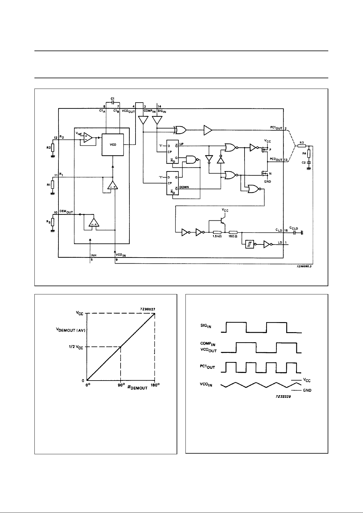
GENERAL DESCRIPTION
The 74HC/HCT7046 are high-speed
Si-gate CMOS devices and are
specified in compliance with JEDEC
standard no. 7.
The 74HC/HCT7046 are
phase-locked-loop circuits that
comprise a linear voltage-controlled
oscillator (VCO) and two different
phase comparators (PC1 and PC2)
with a common signal input amplifier
and a common comparator input.
A lock detector is provided and this
gives a HIGH level at pin 1 (LD) when
the PLL is locked. The lock detector
capacitor must be connected
between pin 15 (C
LD
) and pin 8
(GND). The value of the CLD capacitor
can be determined, using information
supplied in Fig.32. The input signal
can be directly coupled to large
voltage signals, or indirectly coupled
(with a series capacitor) to small
voltage signals. A self-bias input
circuit keeps small voltage signals
within the linear region of the input
amplifiers. With a passive low-pass
filter, the “7046” forms a second-order
loop PLL. The excellent VCO linearity
is achieved by the use of linear
op-amp techniques.
VCO
The VCO requires one external
capacitor C1 (between C1
A
and C1B)
and one external resistor R1
(between R1 and GND) or two
external resistors R1 and R2
(between R1 and GND, and R2 and
GND). Resistor R1 and capacitor C1
determine the frequency range of the
VCO. Resistor R2 enables the VCO
to have a frequency offset if required.
The high input impedance of the VCO
simplifies the design of low-pass
filters by giving the designer a wide
choice of resistor/capacitor ranges. In
order not to load the low-pass filter, a
demodulator output of the VCO input
voltage is provided at pin 10
(DEM
OUT
). In contrast to conventional
techniques where the DEM
OUT
voltage is one threshold voltage lower
than the VCO input voltage, here the
DEM
OUT
voltage equals that of the
VCO input. If DEM
OUT
is used, a load
resistor (RS) should be connected
from DEM
OUT
to GND; if unused,
DEM
OUT
should be left open. The
VCO output (VCO
OUT
) can be
connected directly to the comparator
input (COMPIN), or connected via a
frequency-divider. The VCO output
signal has a duty factor of 50%
(maximum expected deviation 1%), if
the VCO input is held at a constant
DC level. A LOW level at the inhibit
input (INH) enables the VCO and
demodulator, while a HIGH level turns
both off to minimize standby power
consumption.
The only difference between the HC
and HCT versions is the input level
specification of the INH input. This
input disables the VCO section. The
comparators’ sections are identical,
so that there is no difference in the
SIG
IN
(pin 14) or COMPIN (pin 3)
inputs between the HC and HCT
versions.
Phase comparators
The signal input (SIG
IN
) can be
directly coupled to the self-biasing
amplifier at pin 14, provided that the
signal swing is between the standard
HC family input logic levels.
Capacitive coupling is required for
signals with smaller swings.
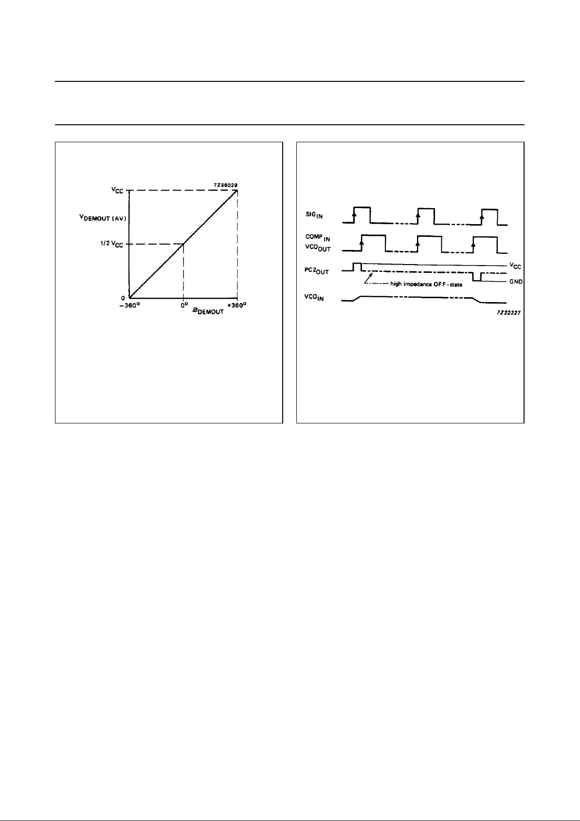
Phase comparator 1 (PC1)
This is an EXCLUSIVE-OR network.
The signal and comparator input
frequencies (fi) must have a 50% duty
factor to obtain the maximum locking
range. The transfer characteristic of
PC1, assuming ripple (f
r
=2fi) is
suppressed,
is:
where V
DEMOUT
is the demodulator
output at pin 10;
V
DEMOUT=VPC1OUT
(via low-pass
filter).
The phase comparator gain
is:
The average output voltage from
PC1, fed to the VCO input via the
low-pass filter and seen at the
demodulator output at pin 10
(V
DEMOUT
), is the resultant of the
phase differences of signals (SIGIN)
and the comparator input (COMPIN)
as shown in Fig.6. The average of
V
DEMOUT
is equal to 1/2 VCC when
there is no signal or noise at SIG
IN
and with this input the VCO oscillates
at the centre frequency (fo). Typical
V
DEMOUT
V
CC
π
---------- -
φ
SIGINφCOMPIN
–()=
K
p
V
CC
π
---------- -
Vr⁄().=
Page 3

December 1990 3
Philips Semiconductors Product specification
Phase-locked-loop with lock detector 74HC/HCT7046A
waveforms for the PC1 loop locked at
fo are shown in Fig.7.
The frequency capture range (2fc) is
defined as the frequency range of
input signals on which the PLL will
lock if it was initially out-of-lock. The
frequency lock range (2fL) is defined
as the frequency range of input
signals on which the loop will stay
locked if it was initially in lock. The
capture range is smaller or equal to
the lock range.
With PC1, the capture range depends
on the low-pass filter characteristics
and can be made as large as the lock
range. This configuration retains lock
even with very noisy input signals.
Typical behaviour of this type of
phase comparator is that it can lock to
input frequencies close to the
harmonics of the VCO centre
frequency.
Phase comparator 2 (PC2)
This is a positive edge-triggered
phase and frequency detector. When
the PLL is using this comparator, the
loop is controlled by positive signal
transitions and the duty factors of
SIGIN and COMPIN are not important.
PC2 comprises two D-type flip-flops,
control-gating and a 3-state output
stage. The circuit functions as an
up-down counter (Fig.5) where SIG
IN
causes an up-count and COMPIN a
down-count. The transfer function of
PC2, assuming ripple (f
r=fi
) is
suppressed,
is:
where V
DEMOUT
is the demodulator
output at pin 10;
V
DEMOUT=VPC2OUT
(via low-pass
filter).
V
DEMOUT
V
CC
4π
---------- -
φ
SIGINφCOMPIN
–()=
The phase comparator gain is:
V
DEMOUT
is the resultant of the initial
phase differences of SIG
IN
and
COMP
IN
as shown in Fig.8. Typical
waveforms for the PC2 loop locked at
f
o
are shown in Fig.9.
When the frequencies of SIG
IN
and
COMP
IN
are equal but the phase of
SIG
IN
leads that of COMPIN, the
p-type output driver at PC2
OUT
is held
“ON” for a time corresponding to the
phase difference (φ
DEMOUT
). When
the phase of SIG
IN
lags that of
COMP
IN
, the n-type driver is held
“ON”.
When the frequency of SIG
IN
is higher
than that of COMPIN, the p-type
output driver is held “ON” for most of
the input signal cycle time, and for
the remainder of the cycle both n and
p- type drivers are “OFF” (3-state). If
the SIGINfrequency is lower than the
COMPIN frequency, then it is the
n-type driver that is held “ON” for
most of the cycle. Subsequently, the
voltage at the capacitor (C2) of the
low-pass filter connected to PC2
OUT
varies until the signal and comparator
inputs are equal in both phase and
frequency. At this stable point the
voltage on C2 remains constant as
the PC2 output is in 3-state and the
VCO input at pin 9 is a high
impedance.
Thus, for PC2, no phase difference
exists between SIGIN and COMP
IN
over the full frequency range of the
VCO. Moreover, the power
dissipation due to the low-pass filter is
reduced because both p and n-type
drivers are “OFF” for most of the
signal input cycle. It should be noted
that the PLL lock range for this type of
phase comparator is equal to the
capture range and is independent of
K
p
V
CC
4π
---------- -
Vr⁄().=
the low-pass filter. With no signal
present at SIG
IN
the VCO adjusts, via
PC2, to its lowest frequency.
APPLICATIONS
• FM modulation and demodulation
• Frequency synthesis and
multiplication
• Frequency discrimination
• Tone decoding
• Data synchronization and
conditioning
• Voltage-to-frequency conversion
• Motor-speed control
Page 4
December 1990 4
Philips Semiconductors Product specification
Phase-locked-loop with lock detector 74HC/HCT7046A
QUICK REFERENCE DATA
GND = 0 V; T
amb
=25°C;
Notes
1. Applies to the phase comparator section only (VCO disabled).
For power dissipation of VCO and demodulator sections see Figs 20, 21 and 22.
2. C
PD
is used to determine the dynamic power dissipation (PD in µW):
PD=CPD× V
CC
2
× fi+∑(CL× V
CC
2
× fo) where:
fi= input frequency in MHz
fo= output frequency in MHz
∑ (CL× V
CC
2
× fo) = sum of outputs
CL= output load capacitance in pF
VCC= supply voltage in V
ORDERING INFORMATION
See
“74HC/HCT/HCU/HCMOS Logic Package Information”
.
SYMBOL PARAMETER CONDITIONS
TYPICAL
UNIT
HC HCT
f
o
VCO centre frequency C1 = 40 pF; R1 = 3 kΩ; VCC= 5 V 19 19 MHz
C
I
input capacitance (pin 5) 3.5 3.5 pF
C
PD
power dissipation capacitance per package notes 1 and 2 24 24 pF
Page 5
December 1990 5
Philips Semiconductors Product specification
Phase-locked-loop with lock detector 74HC/HCT7046A
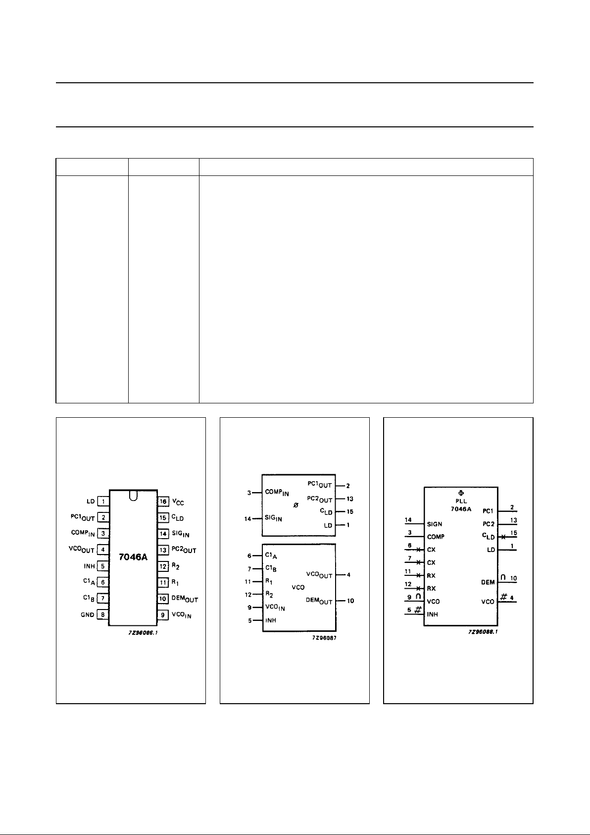
PIN DESCRIPTION
PIN NO. SYMBOL NAME AND FUNCTION
1 LD lock detector output (active HIGH)
2 PC1
OUT
phase comparator 1 output
3 COMP
IN
comparator input
4 VCO
OUT
VCO output
5 INH inhibit input
6C1
A
capacitor C1 connection A
7C1
B
capacitor C1 connection B
8 GND ground (0 V)
9 VCO
IN
VCO input
10 DEM
OUT
demodulator output
11 R
1
resistor R1 connection
12 R
2
resistor R2 connection
13 PC2
OUT
phase comparator 2 output
14 SIG
IN
signal input
15 C
LD
lock detector capacitor input
16 V
CC
positive supply voltage
Fig.1 Pin configuration. Fig.2 Logic symbol. Fig.3 IEC logic symbol.
Page 6
December 1990 6
Philips Semiconductors Product specification
Phase-locked-loop with lock detector 74HC/HCT7046A
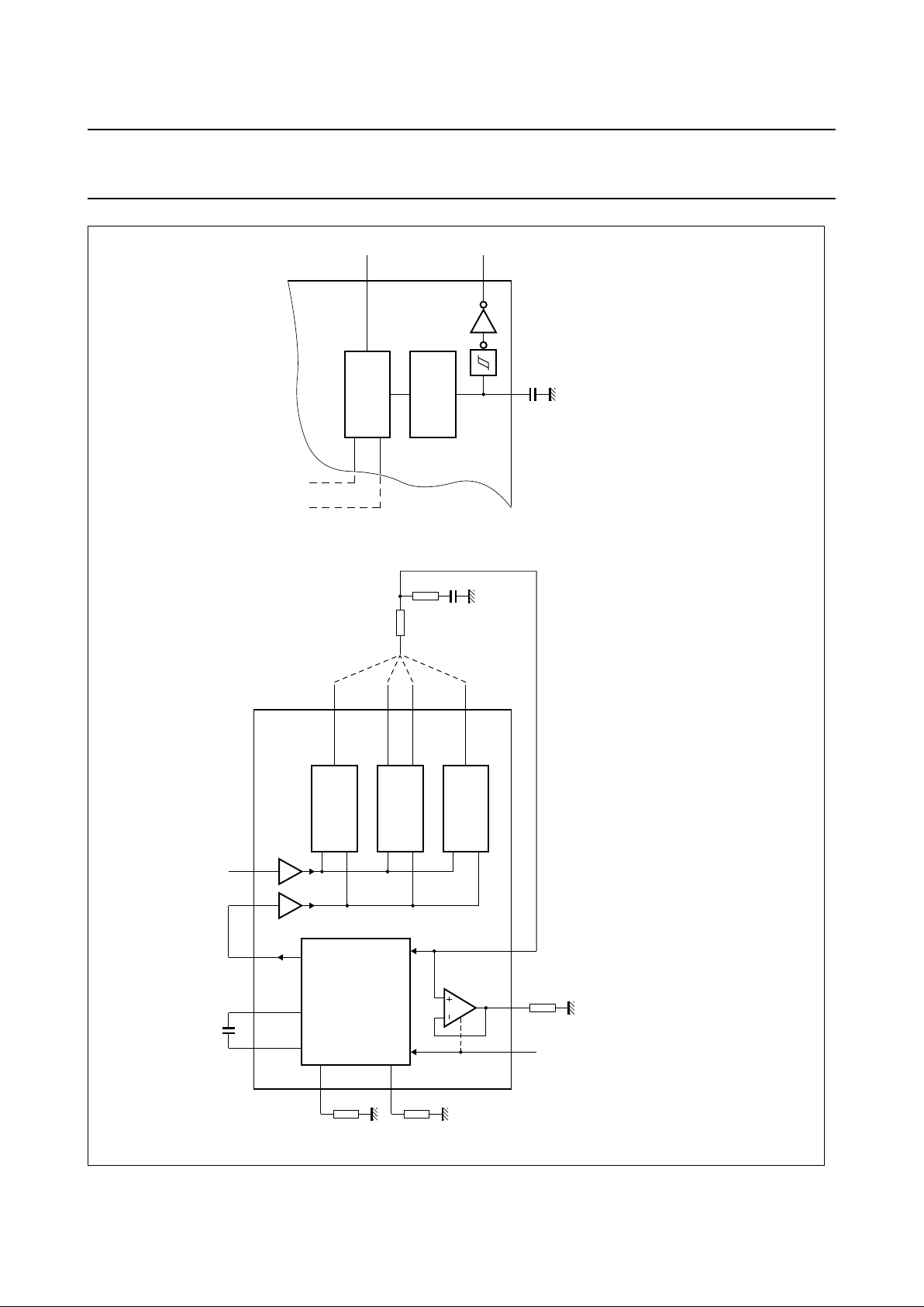
Fig.4 Functional diagram.
MGA847
PHASE
COMPARATOR
2
LOCK
DETECTOR
PC2
OUT
LD
13
1
identical to 4046A
C
LD
C
CLD
15
7046A
PHASE
COMPARATOR
2
PC2
OUT 13
PHASE
COMPARATOR
3
PC3
OUT 15
PHASE
COMPARATOR
1
PC1
OUT
2
PCP
OUT
1
SIG
IN
COMP
IN
V
CO OUT
C1
A
C1
B
DEM
OUTINH
VCO
IN
R
2
R
1
R2
12
11
314476
5109
(a)
(b)
C1
4046A
VCO
R
S
R1
R4
R3
C2
Page 7
December 1990 7
Philips Semiconductors Product specification
Phase-locked-loop with lock detector 74HC/HCT7046A
Fig.5 Logic diagram.
Fig.6 Phase comparator 1: average output
voltage versus input phase difference:
V
DEMOUT
V
PC1OUT
V
CC
π
---------- -
φ
SIGINφCOMPIN
–()==
φ
DEMOUTφSIGINφCOMPIN
–=
Fig.7 Typical waveforms for PLL using phase
comparator 1, loop locked at fo.
Page 8
December 1990 8
Philips Semiconductors Product specification
Phase-locked-loop with lock detector 74HC/HCT7046A
Fig.8 Phase comparator 2: average output
voltage versus input phase difference:
V
DEMOUT
V
PC2OUT
=
V
CC
4π
---------- -
φ
SIGINφCOMPIN
–()=
φ
DEMOUT
φ
SIGINφCOMPIN
–()
˙
.=
Fig.9 Typical waveforms for PLL using phase
comparator 2, loop locked at f
o.
Page 9
December 1990 9
Philips Semiconductors Product specification
Phase-locked-loop with lock detector 74HC/HCT7046A
RECOMMENDED OPERATING CONDITIONS FOR 74HC/HCT
RATINGS
Limiting values in accordance with the Absolute Maximum System (IEC 134)
Voltages are referenced to GND (ground = 0 V)
SYMBOL PARAMETER
74HC 74HCT
UNIT CONDITIONS
min. typ. max. min. typ. max.
V
CC
DC supply voltage 3.0 5.0 6.0 4.5 5.0 5.5 V
V
CC
DC supply voltage if VCO section is
not used
2.0 5.0 6.0 4.5 5.0 5.5 V
V
I
DC input voltage range 0 V
CC
0V
CC
V
V
O
DC output voltage range 0 V
CC
0V
CC
V
T
amb
operating ambient temperature range −40 +85 −40 +85 °C see DC and AC
CHARACTERISTICS
T
amb
operating ambient temperature range −40 +125 −40 +125 °C
tr, t
f
input rise and fall times (pin 5)
6.0
1000
500
400
6.0 500 ns
VCC= 2.0 V
VCC= 4.5 V
VCC= 6.0 V
SYMBOL PARAMETER MIN. MAX. UNIT CONDITIONS
V
CC
DC supply voltage −0.5 +7V
±I
IK
DC input diode current 20 mA for VI<−0.5 V or VI> VCC+ 0.5 V
±I
OK
DC output diode current 20 mA for VO<−0.5 V or VO> VCC+ 0.5 V
±I
O
DC output source or sink current 25 mA for − 0.5 V < VO< VCC+ 0.5 V
±I
CC
;
±I
GND
DC VCC or GND current
50 mA
T
stg
storage temperature range −65 +150 °C
P
tot
power dissipation per package
plastic DIL 750 mW
for temperature range: −40 to +125 °C
74HC/HCT
above +70 °C: derate linearly with 12 mW/K
plastic mini-pack (SO) 500 mW above +70 °C: derate linearly with 8 mW/K
Page 10
December 1990 10
Philips Semiconductors Product specification
Phase-locked-loop with lock detector 74HC/HCT7046A
DC CHARACTERISTICS FOR 74HC
Quiescent supply current
Voltages are referenced to GND (ground = 0 V)
SYMBOL PARAMETER
T
amb
(°C)
UNIT
TEST CONDITIONS
74HC
V
CC
(V)
OTHER+25 −40 to +85 −40 to +125
min. typ. max. min. max. min. max.
I
CC
quiescent supply
current
(VCO disabled)
8.0 80.0 160.0 µA 6.0 pins 3, 5, and 14 at
VCC; pin 9 at GND;
II at pins 3 and 14
to be excluded
Page 11
December 1990 11
Philips Semiconductors Product specification
Phase-locked-loop with lock detector 74HC/HCT7046A
Phase comparator section
Voltages are referenced to GND (ground = 0 V)
SYMBOL PARAMETER
T
amb
(°C)
UNIT
TEST CONDITIONS
74HC
V
CC
(V)
V
I
OTHER+25 −40 to +85 −40 to +125
min. typ. max. min. max. min. max.
V
IH
DC coupled HIGH
level input voltage
SIGIN, COMP
IN
1.5
3.15
4.2
1.2
2.4
3.2
1.5
3.15
4.2
1.5
3.15
4.2
V
2.0
4.5
6.0
V
IL
DC coupled LOW level
input voltage
SIGIN, COMP
IN
0.8
2.1
2.8
0.5
1.35
1.8
0.5
1.35
1.8
0.5
1.35
1.8
V
2.0
4.5
6.0
V
OH
HIGH level output
voltage
LD, PC
nOUT
1.9
4.4
5.9
2.0
4.5
6.0
1.9
4.4
5.9
1.9
4.4
5.9
V
2.0
4.5
6.0
V
IH
or
V
IL
−IO=20µA
−IO=20µA
−IO=20µA
V
OH
HIGH level output
voltage
LD, PC
nOUT
3.98
5.48
4.32
5.81
3.84
5.34
3.7
5.2
V
4.5
6.0
V
IH
or
V
IL
−IO= 4.0 mA
−I
O
= 5.2 mA
V
OL
LOW level output
voltage
LD, PC
nOUT
0
0
0
0.1
0.1
0.1
0.1
0.1
0.1
0.1
0.1
0.1
V
2.0
4.5
6.0
V
IH
or
V
IL
IO=20µA
IO=20µA
IO=20µA
V
OL
LOW level output
voltage
LD, PC
nOUT
0.15
0.16
0.26
0.26
0.33
0.33
0.4
0.4
V
4.5
6.0
V
IH
or
V
IL
IO= 4.0 mA
I
O
= 5.2 mA
±I
I
input leakage current
SIGIN, COMP
IN
3.0
7.0
18.0
30.0
4.0
9.0
23.0
38.0
5.0
11.0
27.0
45.0
µA 2.0
3.0
4.5
6.0
V
CC
or
GND
±I
OZ
3-state
OFF-state current
PC2
OUT
0.5 5.0 10.0 µA 6.0 V
IH
or
V
IL
VO=V
CC
or GND
R
I
input resistance
SIGIN, COMP
IN
800
250
150
kΩ 3.0
4.5
6.0
VI at self-bias
operating point;
∆V
I
= 0.5 V; see
Figs 10, 11 and 12
Page 12
December 1990 12
Philips Semiconductors Product specification
Phase-locked-loop with lock detector 74HC/HCT7046A
VCO section
Voltages are referenced to GND (ground = 0 V)
Note
1. The parallel value of R1 and R2 should be more than 2.7 kΩ. Optimum performance is achieved when R1 and/or R2
are/is > 10 kΩ.
SYM-
BOL
PARAMETER
T
amb
(°C)
UNIT
TEST CONDITIONS
74HC
V
CC
(V)
V
I
OTHER+25 −40 to +85 −40 to +125
min. typ. max. min. max. min. max.
V
IH
HIGH level
input voltage
INH
2.1
3.15
4.2
1.7
2.4
3.2
2.1
3.15
4.2
2.1
3.15
4.2
V
3.0
4.5
6.0
V
IL
LOW level
input voltage
INH
1.3
2.1
2.8
0.9
1.35
1.8
0.9
1.35
1.8
0.9
1.35
1.8
V
3.0
4.5
6.0
V
OH
HIGH level
output voltage
VCO
OUT
2.9
4.4
5.9
3.0
4.5
6.0
2.9
4.4
5.9
2.9
4.4
5.9
V
3.0
4.5
6.0
V
IH
or
V
IL
−IO=20µA
−IO=20µA
−IO=20µA
V
OH
HIGH level
output voltage
VCO
OUT
3.98
5.48
4.32
5.81
3.84
5.34
3.7
5.2
V
4.5
6.0
V
IH
or
V
IL
−IO= 4.0 mA
−IO= 5.2 mA
V
OL
LOW level
output voltage
VCO
OUT
0
0
0
0.1
0.1
0.1
0.1
0.1
0.1
0.1
0.1
0.1
V
3.0
4.5
6.0
V
IH
or
V
IL
IO=20µA
IO=20µA
IO=20µA
V
OL
LOW level
output voltage
VCO
OUT
0.15
0.16
0.26
0.26
0.33
0.33
0.4
0.4
V
4.5
6.0
V
IH
or
V
IL
IO= 4.0 mA
IO= 5.2 mA
V
OL
LOW level output
voltage C1A,C1
B
(test purposes only)
0.40
0.40
0.47
0.47
0.54
0.54
V
4.5
6.0
V
IH
or
V
IL
IO= 4.0 mA
IO= 5.2 mA
±I
I
input leakage current
INH, VCO
IN
0.1 1.0 1.0 µA 6.0
V
CC
or
GND
R1 resistor range
3.0
3.0
3.0
300
300
300
kΩ
3.0
4.5
6.0
note 1
R2 resistor range
3.0
3.0
3.0
300
300
300
kΩ
3.0
4.5
6.0
note 1
C1 capacitor range
40
40
40
no
limit
pF
3.0
4.5
6.0
V
VCOIN
operating voltage
range at VCO
IN
1.1
1.1
1.1
1.9
3.4
4.9
V
3.0
4.5
6.0
over the range
specified for R1;
for linearity see
Figs 18 and 19.
Page 13

December 1990 13
Philips Semiconductors Product specification
Phase-locked-loop with lock detector 74HC/HCT7046A
Demodulator section
Voltages are referenced to GND (ground = 0 V)
SYMBOL PARAMETER
T
amb
(°C)
UNIT
TEST CONDITIONS
74HC
V
CC
(V)
OTHER+25 −40 to +85 −40 to +125
min. typ. max. min. max. min. max.
R
S
resistor range 50
50
50
300
300
300
kΩ 3.0
4.5
6.0
at RS> 300 kΩ
the leakage
current can
influence
V
DEMOUT
V
OFF
offset voltage
VCOIN to V
DEMOUT
±30
±20
±10
mV 3.0
4.5
6.0
VI=V
VCOIN
=
1/2 VCC;
values taken
over RS range;
see Fig.13
R
D
dynamic output
resistance at DEM
OUT
25
25
25
Ω 3.0
4.5
6.0
V
DEMOUT
=
1/2 V
CC
Page 14

December 1990 14
Philips Semiconductors Product specification
Phase-locked-loop with lock detector 74HC/HCT7046A
AC CHARACTERISTICS FOR 74HC
Phase comparator section
GND = 0 V; tr=tf= 6 ns; CL= 50 pF
VCO section
GND = 0 V; t
r=tf
= 6 ns; CL= 50 pF
SYMBOL PARAMETER
T
amb
(°C)
UNIT
TEST CONDITIONS
74HC
V
CC
(V)
OTHER+25 −40 to +85 −40 to +125
min. typ. max. min. max. min. max.
t
PHL
/ t
PLH
propagation delay
SIGIN, COMP
IN
to PC1
OUT
58
21
17
200
40
34
250
50
43
300
60
51
ns 2.0
4.5
6.0
Fig.14
t
PZH
/ t
PZL
3-state output enable
time SIGIN, COMP
IN
to PC2
OUT
74
27
22
280
56
48
350
70
60
420
84
71
ns 2.0
4.5
6.0
Fig.15
t
PHZ
/ t
PLZ
3-state output disable
time SIGIN, COMP
IN
to PC2
OUT
96
35
28
325
65
55
405
81
69
490
98
83
ns 2.0
4.5
6.0
Fig.15
t
THL
/ t
TLH
output transition time 19
7
6
75
15
13
95
19
16
110
22
19
ns 2.0
4.5
6.0
Fig.14
V
I(p-p)
AC coupled input sensitivity
(peak-to-peak value) at
SIGIN or COMP
IN
9
11
15
33
mV 2.0
3.0
4.5
6.0
fi= 1 MHz
SYMBOL
PARAMETER
T
amb
(°C)
UNIT
TEST CONDITIONS
74HC
V
CC
(V)
OTHER
+25 −40 to +85 −40
to +125
min. typ. max. typ. max. min. max.
∆f/T frequency stability
with temperature
change
0.20
0.15
0.14
%/K 3.0
4.5
6.0
V
I=VVCOIN
=1/2 VCC;
R1 = 100 kΩ; R2 = ∞;
C1 = 100 pF; see Fig.16
f
o
VCO centre
frequency
(duty factor = 50%)
7.0
11.0
13.0
10.0
17.0
21.0
MHz 3.0
4.5
6.0
V
VCOIN
= 1/2 VCC;
R1 = 3 kΩ; R2 = ∞;
C1 = 40 pF; see Fig.17
∆f
VCO
VCO frequency
linearity
1.0
0.4
0.3
% 3.0
4.5
6.0
R1 = 100 kΩ; R2 = ∞;
C1 = 100 pF; see Figs 18
and 19
δ
VCO
duty factor at
VCO
OUT
50
50
50
% 3.0
4.5
6.0
Page 15

December 1990 15
Philips Semiconductors Product specification
Phase-locked-loop with lock detector 74HC/HCT7046A
DC CHARACTERISTICS FOR 74HCT
Quiescent supply current
Voltages are referenced to GND (ground = 0 V)
Note
1. The value of additional quiescent supply current (∆I
CC
) for a unit load of 1 is given above.
To determine ∆ICC per input, multiply this value by the unit load coefficient shown in the table below.
SYMBOL PARAMETER
T
amb
(°C)
UNIT
TEST CONDITIONS
74HCT
V
CC
(V)
OTHER+25 −40 to +85 −40 to +125
min. typ. max. min. max. min. max.
I
CC
quiescent supply current
(VCO disabled)
8.0 80.0 160.0 µA 6.0 pins 3, 5 and 14
at VCC; pin 9 at
GND; II at pins 3
and 14 to be
excluded
∆I
CC
additional quiescent
supply current per input
pin for unit load coefficient
is 1 (note 1)
VI=VCC− 2.1 V
100 360 450 490 µA 4.5
to
5.5
pins 3 and 14 at
VCC; pin 9 at
GND; II at pins 3
and 14 to be
excluded
INPUT UNIT LOAD COEFFICIENT
INH 1.00
Page 16

December 1990 16
Philips Semiconductors Product specification
Phase-locked-loop with lock detector 74HC/HCT7046A
Phase comparator section
Voltages are referenced to GND (ground = 0 V)
SYM
BOL
PARAMETER
T
amb
(°C)
UNIT
TEST CONDITIONS
74HCT
V
CC
(V)
V
I
OTHER+25 −40 to +85 −40 to +125
min. typ. max min. max. min. max.
V
IH
DC coupled
HIGH level input voltage
SIGIN, COMP
IN
3.15 2.4 V 4.5
V
IL
DC coupled
LOW level input voltage
SIGIN, COMP
IN
2.1 1.35 V 4.5
V
OH
HIGH level output voltage
LD, PC
nOUT
4.4 4.5 4.4 4.4 V 4.5
V
IH
or
V
IL
−IO=20µA
V
OH
HIGH level output voltage
LD, PC
nOUT
3.98 4.32 3.84 3.7 V 4.5
V
IH
or
V
IL
−IO= 4.0 mA
V
OL
LOW level output voltage
LD, PC
nOUT
0 0.1 0.1 0.1 V 4.5
V
IH
or
V
IL
IO=20µA
V
OL
LOW level output voltage
LD, PC
nOUT
0.15 0.26 0.33 0.4 V 4.5
V
IH
or
V
IL
IO= 4.0 mA
±I
I
input leakage current
SIGIN, COMP
IN
30 38 45 µA 5.5
V
CC
or
GND
±I
OZ
3-state
OFF-state current
PC2
OUT
0.5 5.0 10.0 µA 5.5
V
IH
or
V
IL
VO=V
CC
or GND
R
I
input resistance
SIGIN, COMP
IN
250 kΩ 4.5
VI at self-bias
operating point;
∆V
I
= 0.5 V; see Figs
10, 11 and 12
Page 17

December 1990 17
Philips Semiconductors Product specification
Phase-locked-loop with lock detector 74HC/HCT7046A
DC CHARACTERISTICS FOR 74HCT
VCO section
Voltages are referenced to GND (ground = 0 V)
Note
1. The parallel value of R1 and R2 should be more than 2.7 kΩ. Optimum performance is achieved when R1 and/or R2
are/is > 10 kΩ.
SYMBOL PARAMETER
T
amb
(°C)
UNIT
TEST CONDITIONS
74HCT
V
CC
(V)
V
I
OTHER+25 −40 to +85 −40 to +125
min. typ. max. min. max. min. max.
V
IH
HIGH level input
voltage
INH
2.0 1.6 2.0 2.0 V 4.5
to
5.5
V
IL
LOW level input
voltage
INH
1.2 0.8 0.8 0.8 V 4.5
to
5.5
V
OH
HIGH level output
voltage
VCO
OUT
4.4 4.5 4.4 4.4 V 4.5 V
IH
or
V
IL
−IO=20µA
V
OH
HIGH level output
voltage
VCO
OUT
3.98 4.32 3.84 3.7 V 4.5 V
IH
or
V
IL
−IO= 4.0 mA
V
OL
LOW level output
voltage
VCO
OUT
0 0.1 0.1 0.1 V 4.5 V
IH
or
V
IL
IO=20µA
V
OL
LOW level output
voltage
VCO
OUT
0.15 0.26 0.33 0.4 V 4.5 V
IH
or
V
IL
IO= 4.0 mA
V
OL
LOW level output
voltage C1A, C1
B
(test purposes only)
0.40 0.47 0.54 V 4.5 V
IH
or
V
IL
IO= 4.0 mA
±I
I
input leakage
current
INH, VCO
IN
0.1 1.0 1.0 µA 5.5 V
CC
or
GND
R1 resistor range 3.0 300 kΩ 4.5 note 1
R2 resistor range 3.0 300 kΩ 4.5 note 1
C1 capacitor range 40 no
limit
pF 4.5
V
VCOIN
operating voltage
range at VCO
IN
1.1 3.4 V 4.5 over the range
specified for
R1;
for linearity see
Figs 18 and 19.
Page 18

December 1990 18
Philips Semiconductors Product specification
Phase-locked-loop with lock detector 74HC/HCT7046A
Demodulator section
Voltages are referenced to GND (ground = 0 V)
AC CHARACTERISTICS FOR 74HCT
Phase comparator section
GND = 0 V; t
r=tf
= 6 ns; CL= 50 pF
SYMBOL PARAMETER
T
amb
(°C)
UNIT
TEST CONDITIONS
74HCT
V
CC
(V)
OTHER+25 −40 to +85 −40 to +125
min. typ. max. min. max. min. max.
R
S
resistor range 50 300 kΩ 4.5 at RS> 300 kΩ the
leakage current can
influence V
DEMOUT
V
OFF
offset voltage
VCOIN to V
DEMOUT
±20 mV 4.5 VI=V
VCOIN
= 1/2
VCC; values taken
over RS range;
see Fig.13
R
D
dynamic output
resistance at DEM
OUT
25 Ω 4.5 V
DEMOUT
= 1/2 V
CC
SYMBOL PARAMETER
T
amb
(°C)
UNIT
TEST
CONDITIONS
74HCT
V
CC
(V)
OTHER+25 −40 to +85 −40 to +125
min. typ. max. min. max. min. max.
t
PHL
/ t
PLH
propagation delay
SIGIN, COMP
IN
to PC1
OUT
21 40 50 60 ns 4.5 Fig.14
t
PZH
/ t
PZL
3-state output enable
time SIGIN, COMP
IN
to PC2
OUT
27 56 70 84 ns 4.5 Fig.15
t
PHZ
/ t
PLZ
3-state output disable
time SIGIN, COMP
IN
to PC2
OUT
35 65 81 98 ns 4.5 Fig.15
t
THL
/ t
TLH
output transition time 7 15 19 22 ns 4.5 Fig.14
V
I(p-p)
AC coupled input sensitivity
(peak-to-peak value) at
SIGIN or COMP
IN
15 mV 4.5 fi=
1 MHz
Page 19

December 1990 19
Philips Semiconductors Product specification
Phase-locked-loop with lock detector 74HC/HCT7046A
VCO section
GND = 0 V; t
r=tf
= 6 ns; CL= 50 pF
SYMBOL PARAMETER
T
amb
(°C)
UNIT
TEST CONDITIONS
74HCT
V
CC
(V)
OTHER+25 −40 to +85 −40 to +125
min. typ. max. typ. max. min. max.
∆f/T frequency stability
with temperature
change
0.15 %/K 4.5 V
I=VCOIN
within
recommended
range;
R1 = 100 kΩ;
R2 = ∞;
C1 = 100 pf;
see Fig.16b
f
o
VCO centre frequency
(duty factor = 50%)
11.0 17.0 MHz 4.5 V
VCOIN
= 1/2 VCC;
R1 = 3 kΩ; R2 = ∞;
C1 = 40 pF;
see Fig.17
∆f
VCO
VCO frequency
linearity
0.4 % 4.5 R1 = 100 kΩ;
R2 = ∞;
C1 = 100 pF; see
Figs 18 and 19
δ
VCO
duty factor at VCO
OUT
50 % 4.5
Page 20

December 1990 20
Philips Semiconductors Product specification
Phase-locked-loop with lock detector 74HC/HCT7046A
FIGURE REFERENCES FOR DC CHARACTERISTICS
Fig.10 Typical input resistance curve at SIGIN,
COMPIN.
Fig.11 Input resistance at SIGIN, COMPIN with
∆VI= 0.5 V at self-bias point.
Fig.12 Input current at SIGIN, COMPIN with
∆VI= 0.5 V at self-bias point.
Fig.13 Offset voltage at demodulator output as a
function of VCOIN and RS.
____ RS = 50 kΩ
- - - - RS = 300 kΩ
Page 21

December 1990 21
Philips Semiconductors Product specification
Phase-locked-loop with lock detector 74HC/HCT7046A
AC WAVEFORMS
Fig.14 Waveforms showing input (SIGIN, COMPIN) to output (PC1
OUT
) propagation delays and the output
transition times.
(1) HC : VM= 50%; VI= GND to VCC.
Fig.15 Waveforms showing the 3-state enable and disable times for PC2
OUT
.
(1) HC : VM= 50%; VI= GND to VCC.
Page 22

December 1990 22
Philips Semiconductors Product specification
Phase-locked-loop with lock detector 74HC/HCT7046A
Fig.16 Frequency stability of the VCO as a function of ambient temperature with supply voltage as a parameter.
without offset (R2 = ∞): (a) R1 = 3 kΩ; (b) R1 = 10 kΩ; (c) R1 = 300 kΩ.
- - - - with offset (R1 = ∞): (a) R2 = 3 kΩ; (b) R2 = 10 kΩ; (c) R2 = 300 kΩ.
In (b), the frequency stability for R1 = R2 = 10 kΩ at 5 V is also given (curve A). This curve is set by the total VCO bias current, and is
not simply the addition of the two 10 kΩ stability curves. C1 = 100 pF; V
VCO IN
= 0.5 VCC.
handbook, halfpage
MSB710
T
amb
(oC)
0
150100500−50
−25
−20
−15
−10
−5
5
10
15
20
25
∆
f
(%)
5 V
6 V
3 V
4.5 V
5 V
6 V
V =
CC
3 V
(a)
handbook, halfpage
MSB711
T ( C)
amb
0
f
(%)
o
15010050050
25
20
15
10
5
5
10
15
20
25
∆
5 V
6 V
3 V
5 V
6 V
V =
CC
3 V
(b)
A
handbook, halfpage
MSB712
T ( C)
amb
0
f
(%)
o
15010050050
25
20
15
10
5
5
10
15
20
25
∆
5 V
6 V
(c)
V =
CC
3 V
3 V
6 V
5 V
Page 23

December 1990 23
Philips Semiconductors Product specification
Phase-locked-loop with lock detector 74HC/HCT7046A
AC WAVEFORMS
Fig.16 Continued.
To obtain optimum temperature stability, C1must be a small as possible, but larger than 100 pF.
Page 24

December 1990 24
Philips Semiconductors Product specification
Phase-locked-loop with lock detector 74HC/HCT7046A
Fig.17 Graphs showing VCO frequency (f
VCO
) as a function of the VCO input voltage (V
VCOIN
).
Page 25

December 1990 25
Philips Semiconductors Product specification
Phase-locked-loop with lock detector 74HC/HCT7046A
Fig.18 Definition of VCO frequency linearity:
∆V = 0.5 V over the VCC range:
for VCO linearity
f′
0
f1f2+
2
-------------- -
=
linearity
f′
0f0
–
f′
0
----------------
100× %=
Fig.19 Frequency linearity as a function of R1, C1
and VCC: R2 = ∞ and ∆V = 0.5 V.
Page 26

December 1990 26
Philips Semiconductors Product specification
Phase-locked-loop with lock detector 74HC/HCT7046A
Fig.20 Power dissipation versus the value of R1:
CL= 50 pF; R2 = ∞; V
VCOIN
= 1/2 VCC;
T
amb
=25°C.
____ C1 = 40 pF
- - - - C1 = 1 µF
Fig.21 Power dissipation versus the value of R2:
CL= 50 pF; R1 = ∞; V
VCOIN
= GND = 0 V;
T
amb
=25°C.
____ C1 = 40 pF
- - - - C1 = 1 µF
Fig.22 Typical dc power dissipation of demodulator
section as a function of RS: R1 = R2 = ∞;
T
amb
=25°C; V
VCOIN
= 1/2 VCC.
Page 27

December 1990 27
Philips Semiconductors Product specification
Phase-locked-loop with lock detector 74HC/HCT7046A
APPLICATION INFORMATION
This information is a guide for the approximation of values of external components to be used with the 74HC/HCT7046
in a phase-lock-loop system.
References should be made to Figs 27, 28 and 29 as indicated in the table.
Values of the selected components should be within the following ranges:
R1 between 3 kΩ and 300 kΩ;
R2 between 3 kΩ and 300 kΩ;
R1 + R2 parallel value > 2.7 kΩ;
C1 greater than 40 pF.
SUBJECT
PHASE
COMPARATOR
DESIGN CONSIDERATIONS
VCO frequency characteristic
VCO frequency
without extra
offset
PC1, PC2 With R2 = ∞ and R1 within the range 3 kΩ<R1 < 300 kΩ, the characteristics
of the VCO operation will be as shown in Fig. 23.
(Due to R1, C1 time constant a small offset remains when R2 = ∞.)
Fig. 23 Frequency characteristic of VCO operating without offset:
f
o
= centre frequency; 2fL= frequency lock range.
Selection of R1 and C1
PC1 Given f
o
, determine the values of R1 and C1 using Fig.27.
PC2 Given f
max
and fo, determine the values of R1 and C1 using Fig.27,
use Fig.29 to obtain 2fL and then use this to calculate f
min.
Page 28

December 1990 28
Philips Semiconductors Product specification
Phase-locked-loop with lock detector 74HC/HCT7046A
VCO frequency characteristic
VCO frequency
with extra
offset
PC1, PC2 With R1 and R2 within the ranges 3 kΩ< R1 < 300 kΩ, 3 kΩ<R2 < 300 kΩ,
the characteristics of the VCO operation will be as shown in Fig. 24.
Fig. 24 Frequency characteristic of VCO operating with offset:
f
o
= centre frequency; 2fL= frequency lock range.
Selection of R1, R2 and C1
PC1, PC2 Given f0 and fL, determine the value of product R1C1 by using Fig.29.
Calculate f
off
from the equation f
off=fo
−1.6fL.
Obtain the values of C1 and R2 by using Fig.28.
Calculate the value of R1 from the value of C1 and the product R1C1.
SUBJECT
PHASE
COMPARATOR
DESIGN CONSIDERATIONS
Page 29

December 1990 29
Philips Semiconductors Product specification
Phase-locked-loop with lock detector 74HC/HCT7046A
PLL conditions
with no signal at
the SIGIN input
PC1 VCO adjusts to fo with φ
DEMOUT
=90° and V
VCOIN
= 1/2 VCC (see Fig.6).
PC2 VCO adjusts to f
o
with φ
DEMOUT
= −360° and V
VCOIN
= min. (see Fig.8).
PLL frequency
capture range
PC1, PC2
Loop filter component selection
(a) τ = R3 x C2 (b) amplitude characteristic (c) pole-zero diagram
Fig. 25 Simple loop filter for PLL without offset; R3 ≥ 500 Ω.
(a) τ1 = R3 x C2; (b) amplitude characteristic (c) pole-zero diagram
τ2 = R4 x C2;
τ3 = (R3 + R4) x C2
Fig. 26 Simple loop filter for PLL with offset; R3 + R4 ≥ 500 Ω.
PLL locks on
harmonics at
centre frequency
PC1 yes
PC2 no
noise rejection at
signal input
PC1 high
PC2 low
AC ripple content
when PLL is
locked
PC1 f
r
=2fi, large ripple content at φ
DEMOUT
=90°
PC2 f
r=fi
, small ripple content at φ
DEMOUT
=0°
SUBJECT
PHASE
COMPARATOR
DESIGN CONSIDERATIONS
Page 30

December 1990 30
Philips Semiconductors Product specification
Phase-locked-loop with lock detector 74HC/HCT7046A
Fig.27 Typical value of VCO centre frequency (fo) as a function of C1: R2 = ∞; V
VCOIN
= 1/2 VCC; INH = GND;
T
amb
=25°C.
(1) To obtain optimum VCO performance, C1 must be as small as possible but larger than 100 pF.
(2) Interpolation for various values of R1 can be easily calculated because a constant R1C1 product will produce
almost the same VCO output frequency.
Page 31

December 1990 31
Philips Semiconductors Product specification
Phase-locked-loop with lock detector 74HC/HCT7046A
APPLICATION INFORMATION
Fig.28 Typical value of frequency offset as a function of C1: R1 = ∞; V
VCOIN
= 1/2 VCC; INH = GND; T
amb
=25°C.
(1) To obtain optimum VCO performance, C1 must be as small as possible but larger than 100 pF.
(2) Interpolation for various values of R2 can be easily calculated because a constant R2C2 product will produce
almost the same VCO output frequency.
Page 32

December 1990 32
Philips Semiconductors Product specification
Phase-locked-loop with lock detector 74HC/HCT7046A
Fig.29 Typical frequency lock range (2fL) versus the product R1C1: V
VCOIN
range = 0.9 to (VCC− 0.9) V;
R2 = ∞; VCO gain:
K
V
2f
L
V
VCOIN
range
-------------------------------------
2 π (r/s/V).=
Page 33

December 1990 33
Philips Semiconductors Product specification
Phase-locked-loop with lock detector 74HC/HCT7046A
APPLICATION INFORMATION
Lock-detection circuit
The built-in lock-detection circuit will only work when used
in conjunction with the phase comparator PC2. The
lock-indication is derived from the phase error between
SIG
IN
and COMPIN. The PC2 has a typical phase error of
zero degrees over the entire VCO operating range.
However, to remain in-lock the circuit requires some small
adjustments. The variation is dependent on the loop
parameters and back-lash time (typically 5 ns). Depending
on the application, the phase error can be defined as the
limit, a phase error of greater magnitude would be
considered out-of-lock. An example of an in-lock detection
circuit using the “7046A” is shown in Fig.30.
If the PLL is in-lock, only very small pulses will come from
the “up” or “down” connections of PC2. These pulses are
filtered out by a RC network. A Schmitt trigger produces a
steady state level, a HIGH level indicates an in-lock
condition and a pulsed output indicates an out-of-lock
condition as shown in Fig.31.
Fig.30 An example of an in-lock detection circuit using the “7046A”.
See Fig.31 for input waveform.
Fig.31 Waveforms showing the lock detection process; (a) in-lock; (b) out-of-lock.
(a) (b)
Page 34

December 1990 34
Philips Semiconductors Product specification
Phase-locked-loop with lock detector 74HC/HCT7046A
Fig.32 CLD capacitor value versus typical tLD.
C
LD
= capacitor connected to pin 15
(includes the parasitic input capacitance of the IC, approximately 3.5 pF).
t
LD
= phase difference between SIGIN and COMPIN (positive-going edges).
Page 35

December 1990 35
Philips Semiconductors Product specification
Phase-locked-loop with lock detector 74HC/HCT7046A
The maximum permitted phase error
must be defined, before tLD can be
defined using the following formula:
Using this calculated value in Fig.32,
it is possible to define the value of
CLD, e.g. assuming the phase error is
36° and fIN= 2 MHz:
and using Fig.32, it can be seen that
CLD is 26 pF.
With the addition of one retriggerable
monostable (e.g. “123”, “423” or
“4538”) a steady state LOW and
HIGH indication can be obtained, as
shown in Fig.33.
t
LD
φ
max
360
------------
1
f
IN
------
× .=
t
LD
36°
360
--------- -
1
2MHz
-----------------
× 50 ns,==
Fig.33 Steady state signal for lock indication.
Page 36

December 1990 36
Philips Semiconductors Product specification
Phase-locked-loop with lock detector 74HC/HCT7046A
PLL design example
The frequency synthesizer, used in the design example
shown in Fig.34, has the following parameters:
Output frequency: 2 MHz to 3 MHz
frequency steps : 100 kHz
settling time : 1 ms
overshoot : < 20%
The open-loop gain is H (s) x G (s) = Kp× Kf× Ko× Kn.
Where:
The programmable counter ratio K
n
can be found as
follows:
The VCO is set by the values of R1, R2 and C1,
R2 = 10 kΩ (adjustable). The values can be determined
using the information in the section “DESIGN
CONSIDERATIONS”.
With fo= 2.5 MHz and fL= 500 kHz this gives the following
values (VCC= 5.0 V):
R1 = 10 kΩ
R2 = 10 kΩ
C1 = 500 pF
The VCO gain is:
The gain of the phase comparator is:
The transfer gain of the filter is given by:
Where:
K
p
= phase comparator gain
K
f
= low-pass filter transfer gain
K
o
=Kv/s VCO gain
K
n
= 1/n divider ratio
N
min.
f
out
f
step
-----------
2 MHz
100 kHz
----------------------
20== =
N
max.
f
out
f
step
-----------
3MHz
100 kHz
----------------------
30== =
K
V
2fL2 π××
0.9 V
CC
0.9–()–
----------------------------------------------
1MHz
3.2
-----------------
2 π× 210
6
× r/s/v≈===
K
p
V
CC
4 π×
------------
0.4 V/r.==
K
f
1τ
2
s+
1τ
1
τ
2
+()s+
------------------------------------ -
=
τ
1
R3C2 and τ2R4C2.==
The characteristics equation is:
1 + H (s) × G (s) = 0.
This results in:
The natural frequency ω
n
is defined as follows:
and the damping value ζ is defined as follows:
The overshoot and settling time percentages are now used
to determine ωn. From Fig.35 it can be seen that the
damping ratio ζ = 0.8 will produce an overshoot of less
than 20% and settle to within 5% at ωnt = 4.5. The required
settling time is 1 ms. This results in:
Rewriting the equation for natural frequency results in:
The maximum overshoot occurs at N
max
.:
When C2 = 470 nF, then
R3 is calculated using the damping ratio equation:
s
2
1KpKvK
n
×τ
2
××+
τ
1
τ
2
+()
-----------------------------------------------------
s
K
pKv
× Kn×
τ
1τ2
+()
--------------------------------
0.=++
ω
n
K
p
K
v
×K
n
×
τ
1
τ
2
+()
--------------------------------˙.=
ζ
1
2 ω
n
----------
1K
pKv
× K
n
×τ
2
×+
τ
1
τ
2
+
-----------------------------------------------------
× .=
ω
n
5
t
-- -
5
0.001
-------------- -
510
3
× r/s.== =
τ
1τ2
+()
K
p
K
v
×K
n
×
ω
n
2
--------------------------------
.=
τ
1τ2
+()
0.4 2× 10
6
×
5000
2
30×
---------------------------------
0.0011 s.==
R4
τ1τ2+()2ω
n
×ζ1–××
K
p
K
v
×K
n
×
-----------------------------------------------------------------
790 Ω.==
R3
τ
1
C2
------- -
R4 2 kΩ.=–=
Page 37

December 1990 37
Philips Semiconductors Product specification
Phase-locked-loop with lock detector 74HC/HCT7046A
Note
For an extensive description and application example please refer to application note ordering number
9398 649 90011.
Also available a computer design program for PLL’s ordering number 9398 961 10061.
Since the output frequency is proportional to the VCO control voltage, the PLL frequency response can be observed with
an oscilloscope by monitoring pin 9 of the VCO. The average frequency response, as calculated by the Laplace method,
is found experimentally by smoothing this voltage at pin 9 with a simple RC filter, whose time constant is long compared
to the phase detector sampling rate but short compared to the PLL response time.
Fig.34 Frequency synthesizer.
Fig.35 Type 1, second order frequency step response.
012 4
1.6
1.0
0.6
0
0.8
MGA959
3
1.4
1.2
0.4
0.2
5678
ω
n
t
∆ω
(t)
e
∆ωe/ω
n
∆Φ
(t)
e
∆Φe/ω
n
−0.6
0
0.4
1.0
0.2
−0.4
−0.2
0.6
0.8
= 5.0
ζ
0.5
0.707
1.0
= 0.3
ζ
= 2.0
ζ
Page 38

December 1990 38
Philips Semiconductors Product specification
Phase-locked-loop with lock detector 74HC/HCT7046A
PACKAGE OUTLINES
See
“74HC/HCT/HCU/HCMOS Logic Package Outlines”
.
Fig.36 Frequency compared to the time response.
 Loading...