

Page 1
INTEGRATED CIRCUITS
DATA SH EET
For a complete data sheet, please also download:
•The IC06 74HC/HCT/HCU/HCMOS Logic Family Specifications
•The IC06 74HC/HCT/HCU/HCMOS Logic Package Information
•The IC06 74HC/HCT/HCU/HCMOS Logic Package Outlines
74HC/HCT6323A
Programmable ripple counter with
oscillator; 3-state
Product specification
Supersedes data of December 1990
File under Integrated Circuits, IC06
September 1993
Page 2
Philips Semiconductors Product specification
Programmable ripple counter with
oscillator; 3-state
FEATURES
• 8-pin space saving package
• Programmable 3-stage ripple
counter
• Suitable for over-tone crystal
application up to 50 MHz
(VCC=5V±10%)
• 3-state output buffer
• Two internal capacitors
• Recommended operating range for
use with third overtone crystals
3to6V
• Oscillator stop function (MR)
• Output capability:
bus driver → (15 LSTTL)
• ICC category: MSI.
APPLICATIONS
• Control counters
• Timers
• Frequency dividers
• Time-delay circuits
• CIO (Compact Integrated
Oscillator)
• Third-overtone crystal operation.
GENERAL DESCRIPTION
The HC/HCT6323A are high-speed
Si-gate CMOS devices.
They are specified in compliance with
JEDEC standard no. 7A.
The HC/HCT6323A are oscillators
designed for quartz crystal combined
with a programmable 3-state counter,
a 3-state output buffer and an
overriding asynchronous master
MR). With the two select inputs
reset (
S1 and S2 the counter can be
switched in the divide-by-1, 2, 4 or 8
mode. If left floating the clock is
divided by 8. The oscillator is
designed to operate either in the
fundamental or third overtone mode
depending on the crystal and external
components applied. On-chip
capacitors minimize external
component count for third overtone
crystal applications.
The oscillator may be replaced by an
external clock signal at input X1. In
this event the other oscillator pin (X2)
must be floating. The counter
advances on the negative-going
transition of X1. A LOW level on
resets the counter, stops the oscillator
QUICK REFERENCE DATA
GND = 0 V; T
SYMBOL PARAMETER CONDITIONS
t
PHL/tPLH
f
max
C
I
C
PD
Notes
1. C
is used to determine the dynamic power dissipation (PD in µW):
PD
PD = (CPD x V
where:
fi = input frequency in MHz; fo = output frequency in MHz.
VCC = supply voltage in V; CL = output load capacitance in pF.
I
pull-up
2. For HC and HCT an external clock is applied to X1 with:
tr = tf≤ 6 ns, Vi is GND to VCC, MR = HIGH
I
pull-up
ORDERING INFORMATION
EXTENDED TYPE
NUMBER
74HC/HCT6323AD 8 SO plastic SOT96
74HC/HCT6323A
and sets the output buffer in the
3-state condition. MR can be left
floating since an internal pull-up
resistor will make the MR inactive. In
the HCT version, the MR input and
the two mode select pins S1 and S2
are TTL compatible, but the X1 input
has CMOS input switching levels and
MR
= 25 °C; tr = tf = 6 ns.
amb
propagation delay
X1 to OUT
(S1 = S2 = LOW)
maximum clock
frequency
input capacitance
except X1 and X2
power dissipation
capacitance per
package
2
x fi) + (CL + V
CC
= pull-up currents in µA.
is the summation of −II (µA) of S1 and S2 inputs at the LOW state.
PINS PIN POSITION MATERIAL CODE
may be driven by a TTL output using
a pull-up resistor connected to VCC.
TYP.
HC HCT
CL = 15 pF;
17 17 ns
VCC = 5 V
90 90 MHz
3.5 3.5 pF
+1; notes 1 and 2 54 54 pF
+2; notes 1 and 2 42 42 pF
+4; notes 1 and 2 36 36 pF
+8; notes 1 and 2 33 33 pF
2
CC
x fo) + (I
pull-up
x VCC)
PACKAGE
UNIT
September 1993 2
Page 3
Philips Semiconductors Product specification
Programmable ripple counter with
oscillator; 3-state
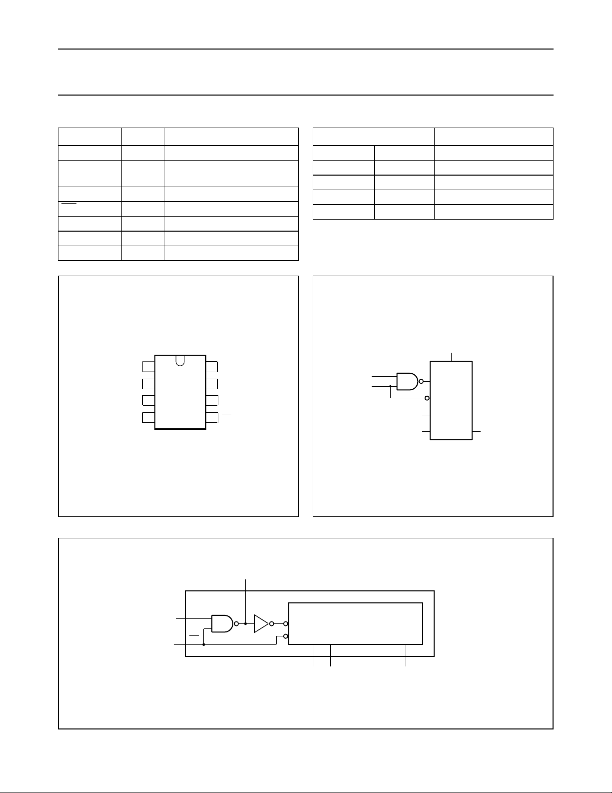
PINNING
SYMBOL PIN DESCRIPTION
OUT 1 counter output
S1 - S2 3, 2 mode select inputs for divide
by 1, 2, 4 or 8
GND 4 ground (0 V)
MR 5 master reset (active LOW)
X2 6 oscillator pin
X1 7 clock input/oscillator pin
V
CC
handbook, halfpage
8 positive supply
1
OUT
2
S2
6323A
3
S1
GND
4
MBA343
V
8
CC
X1
7
X2
6
5
MR
74HC/HCT6323A
FUNCTION TABLE
INPUTS OUTPUTS
S1 S2 OUT
00 f
01 f
10 f
11 f
handbook, halfpage
X1
7
5
MR
3
21
6
X2
CP
C
D
S1
OUT
S2
MBA344
i
/2
i
/4
i
/8
i
Fig.1 Pin configuration.
6
handbook, full pagewidth
7
5
X1
MBA350
X2
CP
C
D
Fig.3 Functional diagram.
September 1993 3
Fig.2 IEC logic symbol.
3 - STAGE BINARY COUNTER
AND DECODER
OUTS1 S2MR
32 1
Page 4
Philips Semiconductors Product specification
Programmable ripple counter with
oscillator; 3-state
handbook, full pagewidth
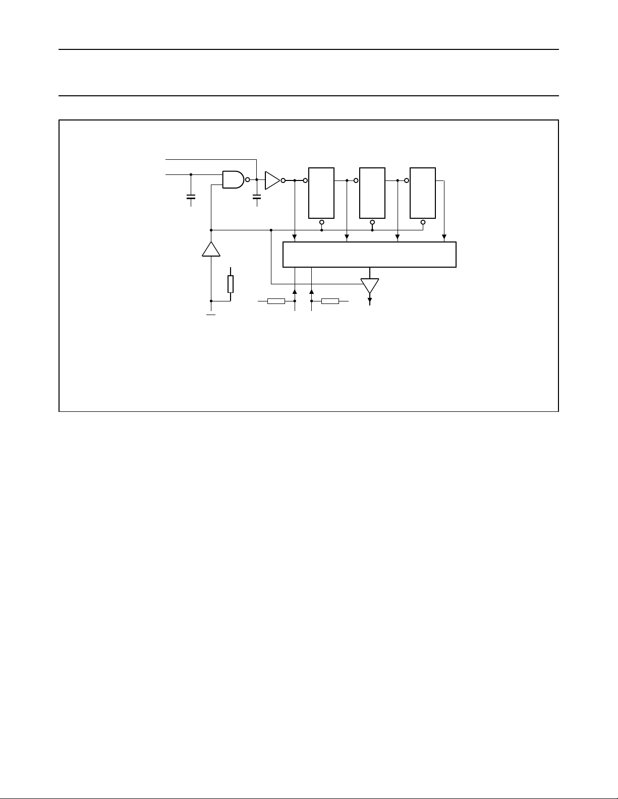
Internal capacitors typical 7 pF each. Including
stray capacitors on pin X1 and X2, total capacitance
will be typical 12 pF per pin.
X2
X1
7 pF
MR
7 pF
V
CC
V
CC
V
CC
(1)
V
CC
74HC/HCT6323A
QCP
S1 S2
FF
R
V
CC
(1)
QCP
FF
R
DECODER
OUT
QCP
FF
R
MBA349
Fig.4 Logic diagram.
September 1993 4
Page 5
Philips Semiconductors Product specification
Programmable ripple counter with
oscillator; 3-state
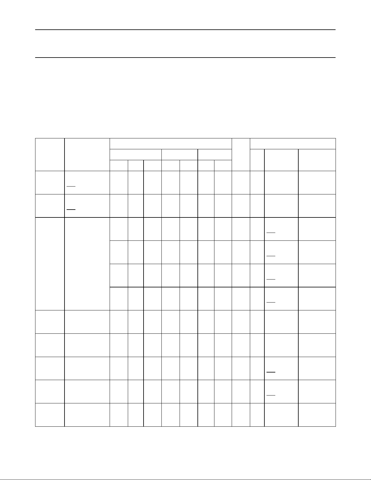
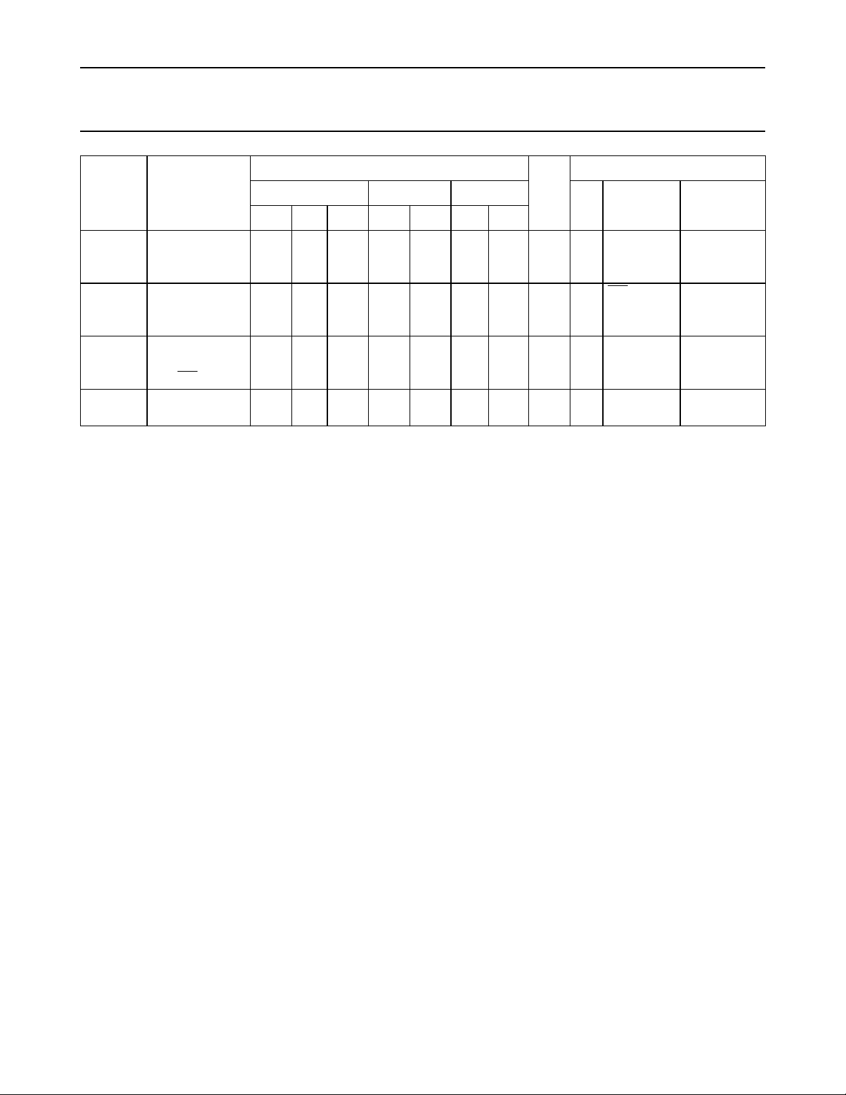
DC CHARACTERISTICS FOR 74HC
For the DC characteristics see
Output capability: non-standard; bus driver (except for X2)
ICC category: MSI.
Voltages are referenced to GND (ground = 0 V).
DC CHARACTERISTICS FOR 74HC
SYMBOL PARAMETER
V
IH
HIGH level
input voltage
MR, X1 input
V
IL
LOW level
input voltage
MR, X1 input
V
OH
HIGH level
output voltage
X2 output
V
OH
HIGH level
output voltage
OUT
V
OH
HIGH level
output voltage
OUT
V
OL
LOW level
output voltage
X2 output
V
OL
LOW level
output voltage
OUT
“74HC/HCT/HCU/HCMOS Logic Family Specifications”
(°C)
T
amb
25 −40 to 85 −40 to 125
MIN TYP MAX MIN MAX MIN MAX
1.5
3.15
4.2
−
−
−
3.98
5.48−−
3.98
5.48−−
1.9
4.4
5.9
1.9
4.4
5.9
1.9
4.4
5.9
3.98
5.48−−
−
−
−
−
−
−
−
−
1.2
2.4
3.2
0.8
2.1
2.8
2.0
4.5
6.0
2.0
4.5
6.0
2.0
4.5
6.0
−
−
0
0
0
0
0
0
−
−
−
0.5
1.35
1.80
−
−
−
−
−
−
−
−
−
−
−
−
−
−
−
0.26
0.26−−
0.1
0.1
0.1
0.1
0.1
0.1
1.5
3.15
4.2
−
−
−
3.84
5.34−−
3.84
5.34−−
1.9
4.4
5.9
1.9
4.4
5.9
1.9
4.4
5.9
3.84
5.34−−
−
−
−
−
−
−
−
−
−
0.5
1.35
1.8
−
−
−
−
−
−
−
−
−
0.33
0.33−−
0.1
0.1
0.1
0.1
0.1
0.1
1.50
3.15
4.20
−
−
−
3.7
5.2−−
3.7
5.2−−
1.9
4.4
5.9
1.9
4.4
5.9
1.9
4.4
5.9
3.7
5.2−−
−
−
−
−
−
−
−
−
−
0.5
1.35
1.8
−
−
−
−
−
−
−
−
−
0.4
0.4VV
0.1
0.1
0.1
0.1
0.1
0.1
UNIT
V
V
V
V
V
V
V
V
V
V
V
V
V
V
V
V
V
V
V
V
V
V
V
V
V
V
V
74HC/HCT6323A
.
TEST CONDITION
V
CC
(V)
2.0
4.5
6.0
2.0
4.5
6.0
4.5
6.0
4.5
6.0
2.0
4.5
6.0
2.0
4.5
6.0
2.0
4.5
6.0
4.5
6.0
4.5
6.0
2.0
4.5
6.0
2.0
4.5
6.0
V
I
X1 = GND
and
MR = V
X1 = V
CC
CC
and
MR = GND
X1 = GND
and
MR = V
X1 = V
CC
CC
and
MR = GND
VIH or V
VIH or V
X1 = V
ILIO
ILIO
CC
and
MR = V
X1 = V
CC
CC
and
MR = V
VIH or V
CC
ILIO
IO = −2.6 mA
IO = −3.3 mA
IO = −2.6 mA
IO = −3.3 mA
−IO = 20 µA
IO = −20 µA
IO = −20 µA
IO = −20 µA
IO = −20 µA
IO = −20 µA
IO = −20 µA
IO = −20 µA
IO = −7.8 mA
IO = 2.6 mA
IO = 3.3 mA
IO = 20 µA
IO = 20 µA
IO = 20 µA
IO = 20 µA
IO = 20 µA
OTHER
= −20 µA
= −6 mA
= 20 µA
September 1993 5
Page 6
Philips Semiconductors Product specification
Programmable ripple counter with
oscillator; 3-state
SYMBOL PARAMETER
V
OL
LOW level
output voltage
OUT
±I
LI
input leakage
current X1
−I
I
input pull-up
current S1, S2
and MR
I
CC
quiescent
supply current
MIN TYP MAX MIN MAX MIN MAX
−
−
−−0.1 − 1 − 1 µA 6.0 MR = V
5 30 100 −−−−µA 6.0 GND see Fig.11
−−8−80 − 160 µA 6.0 VCC or
25 −40 to 85 −40 to 125
−
0.26
−
0.26−−
T
amb
(°C)
0.33
0.33−−
0.4
0.4VV
UNIT
74HC/HCT6323A
TEST CONDITION
V
CC
(V)
4.5
6.0
V
VIH or V
S1 = V
S2 = V
GND
I
ILIO
IO = 7.8 mA
CC
CC
CC
and Fig.12
IO = 0
OTHER
= 6 mA
September 1993 6
Page 7
Philips Semiconductors Product specification
Programmable ripple counter with
oscillator; 3-state
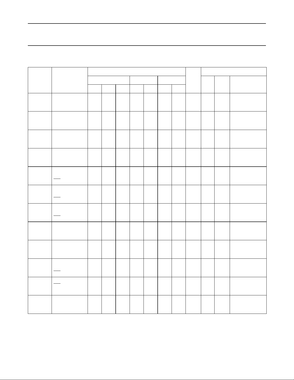
AC CHARACTERISTICS FOR 74HC
GND = 0 V; t
SYMBOL PARAMETER
t
PHL/tPLH
t
PHL/tPLH
t
PHL/tPLH
t
PHL/tPLH
t
PLZ/tPHZ
t
PZL
t
PZH
t
THL/tTLH
t
W
t
W
t
rem
f
max
= tf = 6 ns; CL = 50 pF.
r
MIN TYP MAX MIN MAX MIN MAX
propagation
delay X1 to
OUT divide by 1
propagation
delay X1 to
OUT divide by 2
propagation
delay X1 to
OUT divide by 4
propagation
delay X1 to
OUT divide by 8
3-state output
disable time
MR to OUT
3-state output
enable time
MR to OUT
3-state output
enable time
MR to OUT
−
−
−
−
−
−
−
−
−
−
−
−
−
−
−
−
−
−
−
−
−
output
transition time−−
−
clock pulse
width X1,
HIGH or LOW
master reset
pulse width
MR; LOW
removal time
MR to X1
50
10
9
80
16
14
100
20
17
maximum clock
pulse frequency1050
59
25 −40 to 85 −40 to 125
61
185
22
37
19
31
74
235
27
47
23
40
91
285
33
57
28
48
105
335
38
67
32
57
75
150
15
30
13
26
36
150
13
30
11
26
61
200
22
40
19
34
14
60
5
12
4
10
17
−
6.0
−
5
−
22
−
8
−
7
−
19
−
7
−
6.0
−
17
−
85
−
100
−
T
amb
−
−
−
−
−
−
−
−
−
−
−
−
−
−
−
−
−
−
−
−
−
−
−
−
60
12
10
100
20
17
125
25
21
8
40
47
(°C)
230
46
39
290
58
49
355
71
60
415
83
71
185
37
31
185
37
31
250
50
43
75
15
13
−
−
−
−
−
−
−
−
−
−
−
−
−
−
−
−
−
−
−
−
−
−
−
−
−
−
−
−
−
−
−
−
−
−
−
−
75
15
13
120
24
20
150
30
26
6.6
33
39
275
55
47
350
70
60
425
85
72
500
100
85
225
45
38
225
45
38
300
60
51
90
19
15
−
−
−
−
−
−
−
−
−
−
−
−
UNIT
ns
ns
ns
ns
ns
ns
ns
ns
ns
ns
ns
ns
ns
ns
ns
ns
ns
ns
ns
ns
ns
ns
ns
ns
ns
ns
ns
ns
ns
ns
ns
ns
ns
MHz
MHz
MHz
74HC/HCT6323A
TEST CONDITION
V
CC
(V)
2.0
V
Fig.7 S1 = GND
4.5
6.0
2.0
Fig.7 S1 = GND
4.5
6.0
2.0
Fig.7 S1 = V
4.5
6.0
2.0
Fig.7 S1 = V
4.5
6.0
2.0
Fig.8
4.5
6.0
2.0
Fig.8
4.5
6.0
2.0
Fig.8 note 1
4.5
6.0
2.0
Fig.7
4.5
6.0
2.0
Fig.7
4.5
6.0
2.0
Fig.9
4.5
6.0
2.0
Fig.9
4.5
6.0
2.0
Fig.7
4.5
6.0
I
OTHER
S2 = GND
S2 = V
CC
CC
S2 = GND
CC
S2 = V
CC
Note to the 74HC AC Characteristics
1. t
only applicable in the divide-by-1 mode and X1 must be HIGH.
PZH
September 1993 7
Page 8
Philips Semiconductors Product specification
Programmable ripple counter with
oscillator; 3-state
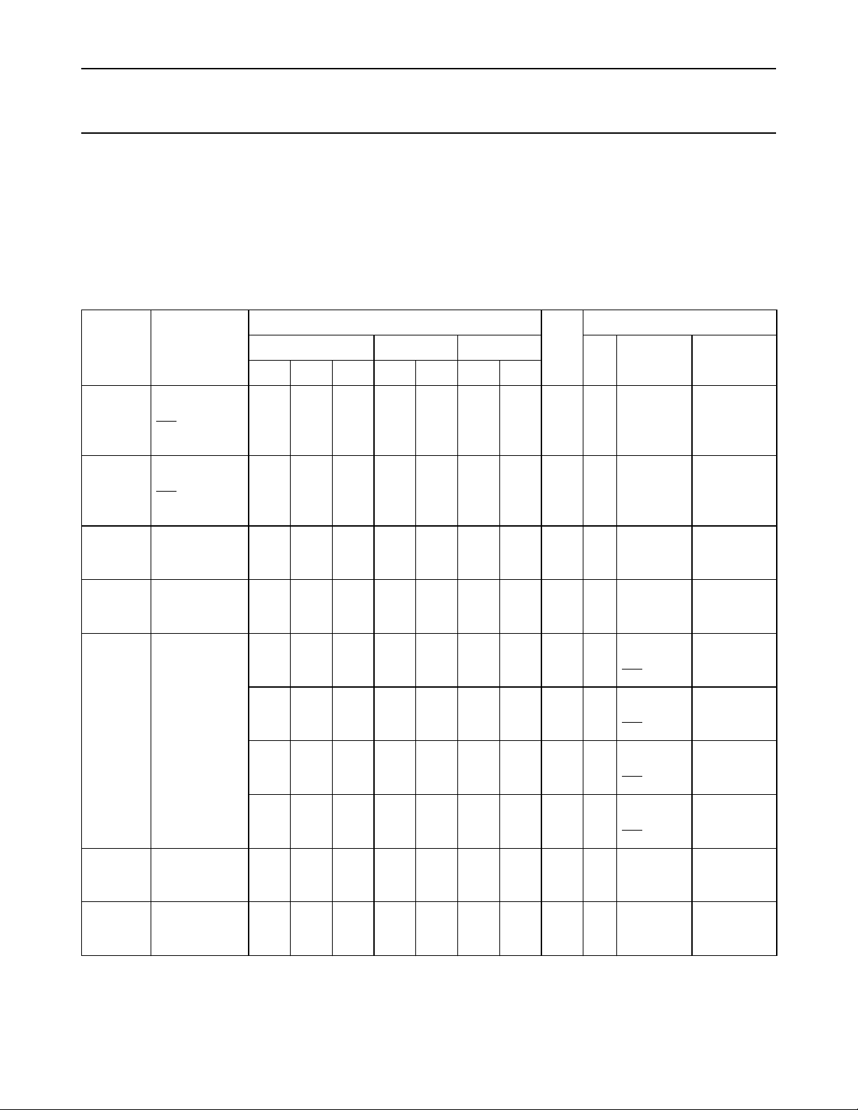
DC CHARACTERISTICS FOR 74HCT
For the DC characteristics see
Output capability: bus driver (except for X2).
ICC category: MSI.
Voltages are referenced to GND (ground = 0 V).
SYMBOL PARAMETER
V
IH
HIGH level
input voltage
MR, S1 and
S2 inputs
V
IL
LOW level
input voltage
MR, S1 and
S2 inputs
V
IH
HIGH level
input voltage
X1 input
V
IL
LOW level
input voltage
X1 input
V
OH
HIGH level
output voltage
X2 output
V
OH
HIGH level
output voltage
OUT
V
OH
HIGH level
output voltage
OUT
“74HC/HCT/HCU/HCMOS Logic Family Specifications”
25 −40 to 85 −40 to 125
MIN TYP MAX MIN MAX MIN MAX
2.0 −−2.0 − 2.0 − V 4.5
−−0.8 − 0.8 − 0.8 V 4.5
3.15
3.85−−
−
−
−
−
−
1.35
−
1.65−−
3.98 −−3.84 − 3.7 − V 4.5 X1 = GND
3.98 −−3.84 − 3.7 − V 4.5 X1 = V
4.4 4.5 − 4.4 − 4.4 − V 4.5 X1 = GND
4.4 4.5 − 4.4 − 4.4 − V 4.5 X1 = V
4.4 4.5 − 4.4 − 4.4 − V 4.5 VIH or V
3.98 −−3.84 − 3.7 − V 4.5 VIH or V
T
amb
3.15
3.85−−
(°C)
1.35
1.65−−
3.15
3.85−−
1.35
1.65VV
UNIT
V
V
74HC/HCT6323A
.
TEST CONDITION
V
CC
(V)
to
5.5
to
5.5
4.5
5.5
4.5
5.5
V
I
and
MR = V
CC
CC
and
MR = GND
and
MR = V
CC
CC
and
MR = GND
ILIO
ILIO
IO = −2.6 mA
IO = −2.6 mA
IO = −20 µA
IO = −20 mA
OTHER
= −20 µA
= −6 mA
September 1993 8
Page 9
Philips Semiconductors Product specification
Programmable ripple counter with
oscillator; 3-state
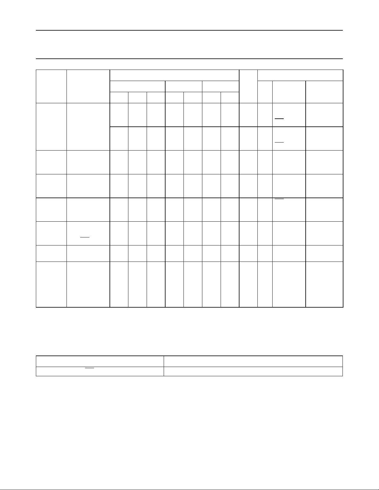
SYMBOL PARAMETER
V
OL
LOW level
output
voltage X2
output
V
OL
LOW level
output voltage
OUT
V
OL
LOW level
output voltage
OUT
±I
LI
input leakage
current
−I
I
input pull-up
current S1, S2
and MR
I
CC
quiescent
supply current
∆I
CC
additional
quiescent
supply current
per input pin
for unit load
coefficient is 1
MIN TYP MAX MIN MAX MIN MAX
−−0.26 − 0.33 − 0.4 V 4.5 X1 = V
− 0 0.1 − 0.1 − 0.1 V 4.5 X1 = V
− 0 0.1 − 0.1 − 0.1 V 4.5 VIH or V
−−0.26 − 0.33 − 0.4 V 4.5 VIH or V
−−0.1 − 1.0 − 1.0 µA 5.5 MR = V
5 25 100 −−−−µA 5.5 GND see Fig.11
−−8−80 − 160 µA 5.5 VCC or
− 100 360 − 450 − 490 µA 5.5 VCC or
25 −40 to 85 −40 to 125
T
amb
(°C)
UNIT
74HC/HCT6323A
TEST CONDITION
V
CC
(V)
V
and
MR = V
and
MR = V
S1 = V
S2 = V
GND
GND
I
CC
CC
CC
CC
ILIO
ILIO
CC;
CC;
CC
OTHER
IO = 2.6 mA
IO = 20 µA
= 20 µA
= 6 mA
and Fig.12
Io=0
other inputs
at VCC or
GND; Io=0;
(note 1)
Note to the HCT DC Characteristics
1. The value of additional quiescent supply current (∆ICC) for unit load of 1 is given in the family specifications.
To determine ∆ICC per input, multiply this value by the unit load coefficient shown in the table below.
UNIT LOAD COEFFICIENT
INPUT UNIT LOAD COEFFICIENT
MR, S1, S2 0.40
September 1993 9
Page 10
Philips Semiconductors Product specification
Programmable ripple counter with
oscillator; 3-state
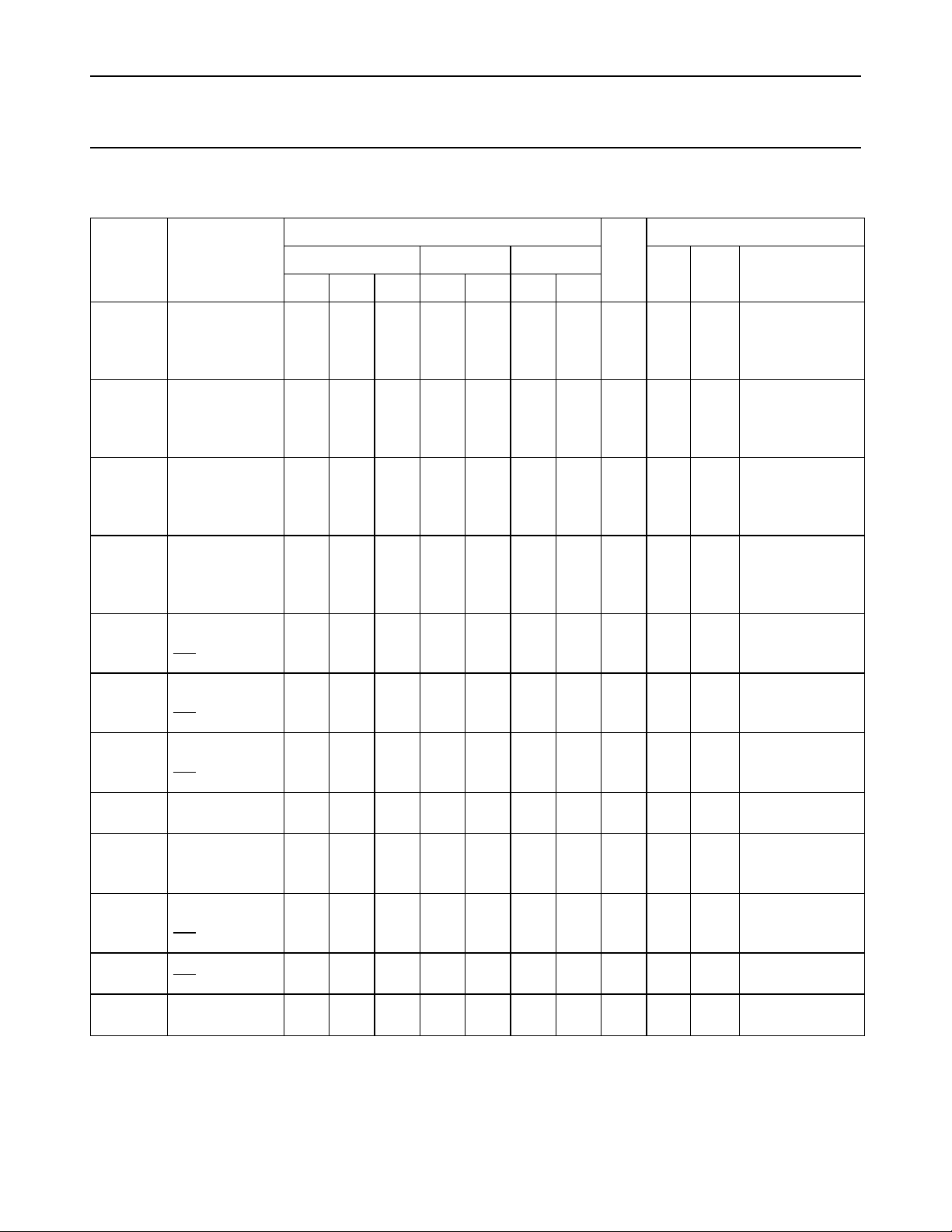
AC CHARACTERISTICS FOR 74HCT
GND = 0 V; t
SYMBOL PARAMETER
t
PHL/tPLH
t
PHL/tPLH
t
PHL/tPLH
t
PHL/tPLH
t
PLZ/tPHZ
t
PZ
t
PZH
t
THL/tTLH
t
W
t
W
t
rem
f
max
= tf = 6 ns; CL = 50 pF
r
MIN TYP MAX MIN MAX MIN MAX
propagation
− 24 40 − 50 − 60 ns 4.5 Fig.7 S1 = GND
delay X1 to
OUT
divide-by-1
propagation
− 29 50 − 62 − 75 ns 4.5 Fig.7 S1 = GND
delay X1 to
OUT
divide-by-2
propagation
− 35 60 − 75 − 90 ns 4.5 Fig.7 S1 = V
delay X1 to
OUT
divide-by-4
propagation
− 40 70 − 87 − 105 ns 4.5 Fig.7 S1 = V
delay X1 to
OUT
divide-by-8
3-state output
− 21 35 − 43 − 52 ns 4.5 Fig.8
disable time
MR to OUT
3-state output
− 16 30 − 37 − 45 ns 4.5 Fig.8
enable time
MR to OUT
3-state output
− 22 38 − 47 − 57 ns 4.5 Fig.8 see note 1
enable time
MR to OUT
output
− 512−15 − 19 ns 4.5 Fig.7
transition time
clock pulse
10 6 − 12 − 15 − ns 4.5 Fig.7
width X1,
HIGH or LOW
master reset
16 8 − 20 − 24 − ns 4.5 Fig.9
pulse width
MR; LOW
removal time
24 12 − 30 − 36 − ns 4.5 Fig.9
MR to X1
maximum clock
50 85 − 40 − 33 − MHz 4.5 Fig.7
pulse frequency
25 −40 to 85 −40 to 125
T
amb
(°C)
UNIT
74HC/HCT6323A
TEST CONDITION
V
CC
(V)
V
I
OTHER
S2 = GND
S2 = V
CC
CC
S2 = GND
CC
S2 = V
CC
Note to the 74HCT AC Characteristics
1. t
only applicable in the divide-by-1 mode and X1 must be HIGH.
PZH
September 1993 10
Page 11
Philips Semiconductors Product specification
Programmable ripple counter with
oscillator; 3-state
R = 560 kΩ
input
bias
V
CC
100 F
output
µ
A
MGA645
i
o
GND
handbook, halfpage
v
i
(f = 1 kHz)
0.47 F
µ
handbook, halfpage
g
fs
(mA/V)
24
20
16
12
74HC/HCT6323A
MBA331
8
4
0
0123456
VCC (V)
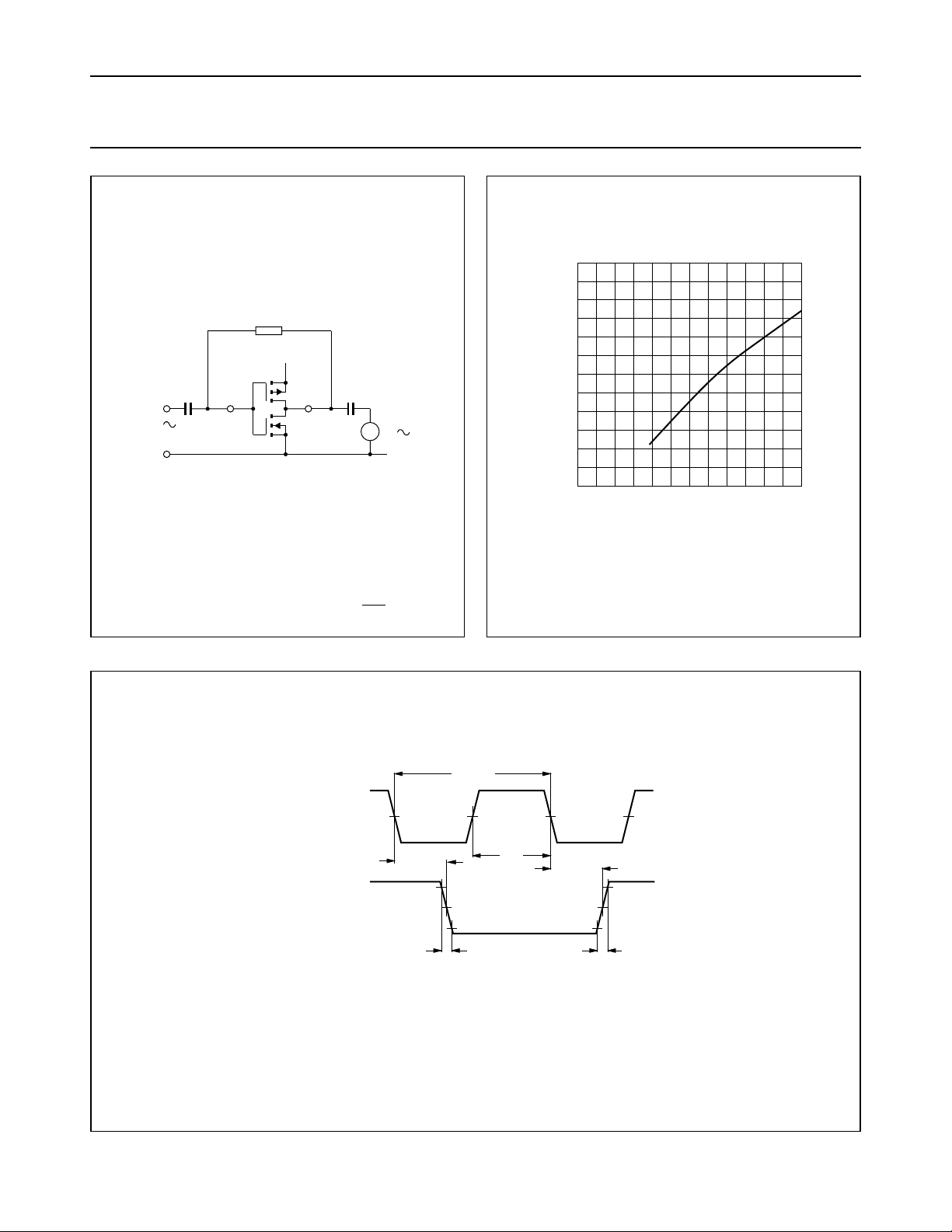
Fig.5 Test set-up for measuring forward
transconductance gfs = dio/dvi at
vo is constant (see also Fig.6); MR = HIGH.
handbook, full pagewidth
X1 INPUT
OUT OUTPUT
(1) HC : VM= 50%; VI= GND to VCC.
HCT : V
= 1.3 V; VI= GND to 3 V.
M
Fig.6 Typical forward transconductance gfs as a
function of the supply voltage Vcc at
T
=25°C.
amb
1/f max
(1)
V
M
t
t
PHL
V
W
(1)
M
t
THL
t
PLH
t
TLH
MBA318
Fig.7 Waveforms showing the clock (X1) to output (OUT) propagation delays, the clock pulse width,
the output transition times and the maximum clock frequency.
September 1993 11
Page 12
Philips Semiconductors Product specification
Programmable ripple counter with
oscillator; 3-state
handbook, full pagewidth
90 %
MR INPUT
OUTPUT
LOW - to - OFF
OFF - to - LOW
OUTPUT
HIGH - to - OFF
OFF - to - HIGH
MBA319
(1)
V
M
t
f
10 %
t
PLZ
t
PHZ
outputs
enabled
90 %
t
outputs
disabled
74HC/HCT6323A
r
t
PZL
(1)
V
M
t
PZH
(1)
V
M
outputs
enabled
(1) HC : VM= 50%; VI= GND to VCC.
HCT : V
= 1.3 V; VI= GND to 3 V.
M
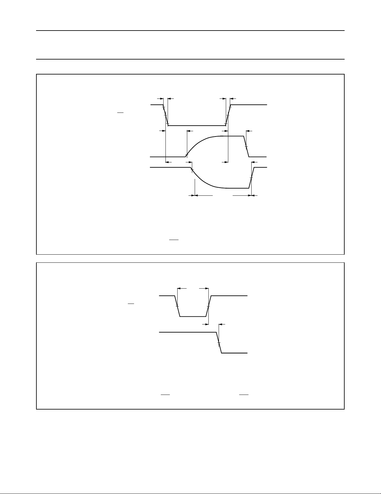
Fig.8 Waveforms showing the input MR to output OUT, 3-state enable and disable times.
handbook, halfpage
(1) HC : VM= 50%; VI= GND to VCC.
HCT : V
= 1.3 V; VI= GND to 3 V.
M
Fig.9 Waveforms showing the MR minimum pulse width and MR to X1 removal time.
MR INPUT
X1 INPUT
t
W
(1)
V
M
t
rem
(1)
V
M
MBA323
September 1993 12
Page 13
Philips Semiconductors Product specification
Programmable ripple counter with
oscillator; 3-state
APPLICATION INFORMATION
handbook, halfpage
5
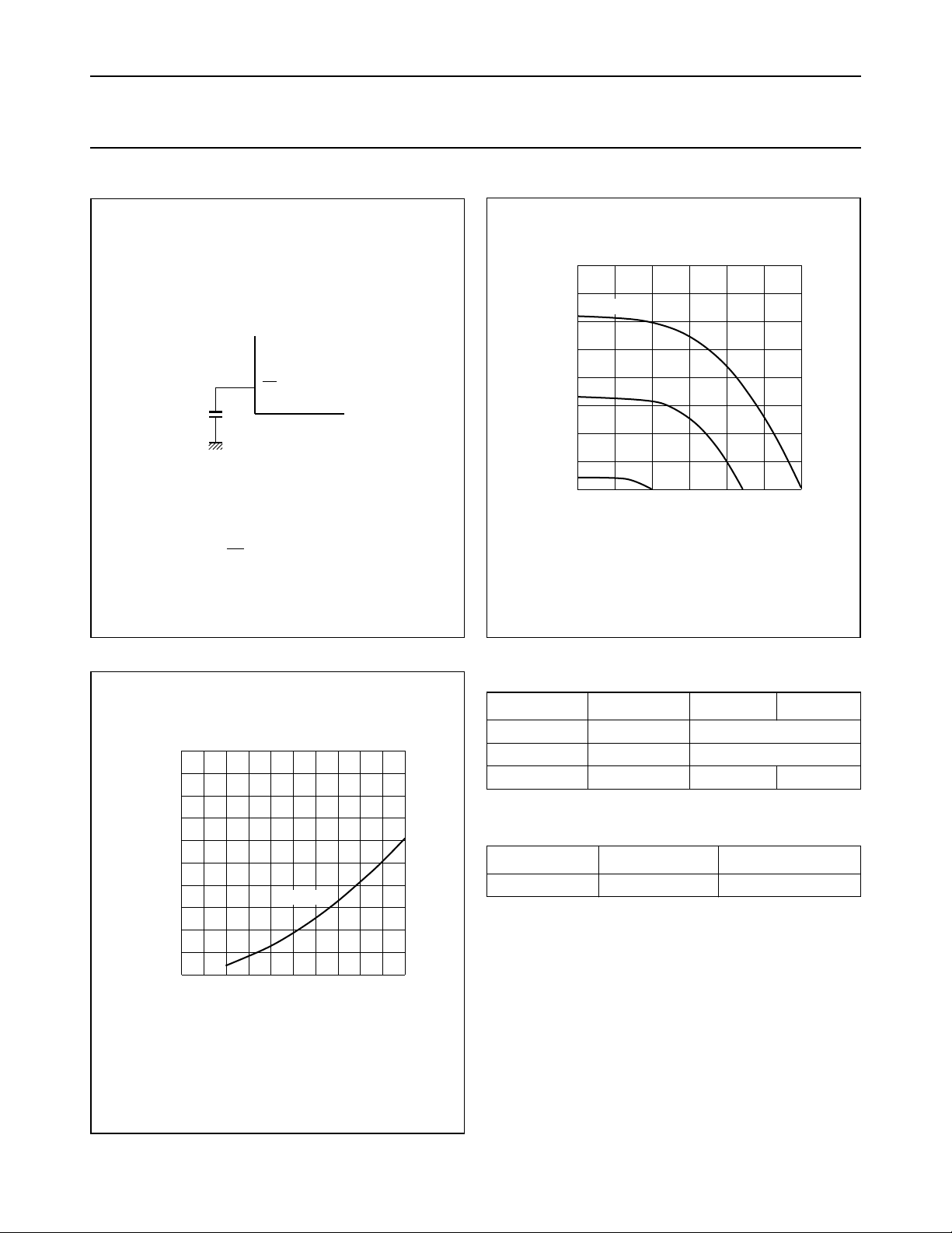
The input pull-up current is used to create a
power-on delay time at
MR.
6323A
MR
MBA348
handbook, halfpage
−I
(µA)
40
I
30
20
10
74HC/HCT6323A
VCC = 6 V
4.3 V
2 V
0
123456
0
MBA347
V
(V)
I
handbook, halfpage
−I
(µA)
I
Fig.10 Power-on reset.
50
40
30
20
10
0
12345 6
VI = 0 V
MBA346
VCC (V)
Fig.11 Typical input pull-up current as a function
of the input voltage (VI).
Table 1 Typical application values
f (MHz) R2 (kΩ) C1 (pF) C2 (pF)
1 4.7 47 to 68
10 2.2 47 to 68
25 1 33 33
Table 2 Typical Application Values
f (MHz) R
(kΩ) C1 (pF)
bias
50 3.0 4.7
Fig.12 Typical input pull-up current as a function of
the supply voltage (VCC).
September 1993 13
Page 14
Philips Semiconductors Product specification
Programmable ripple counter with
oscillator; 3-state
handbook, halfpage
C1
MR (from logic)
X1
7
100 kΩ to 1
22 to
37 pF
R
bias
MΩ
X2
6
R2
2.2
kΩ
100 pFC2
MBA328 - 1
handbook, halfpage
C1
MR (from logic)
X1
7
1 to 10 pF
(optional)
74HC/HCT6323A
X2
R
bias
3 kΩ
6
MBA329 - 1
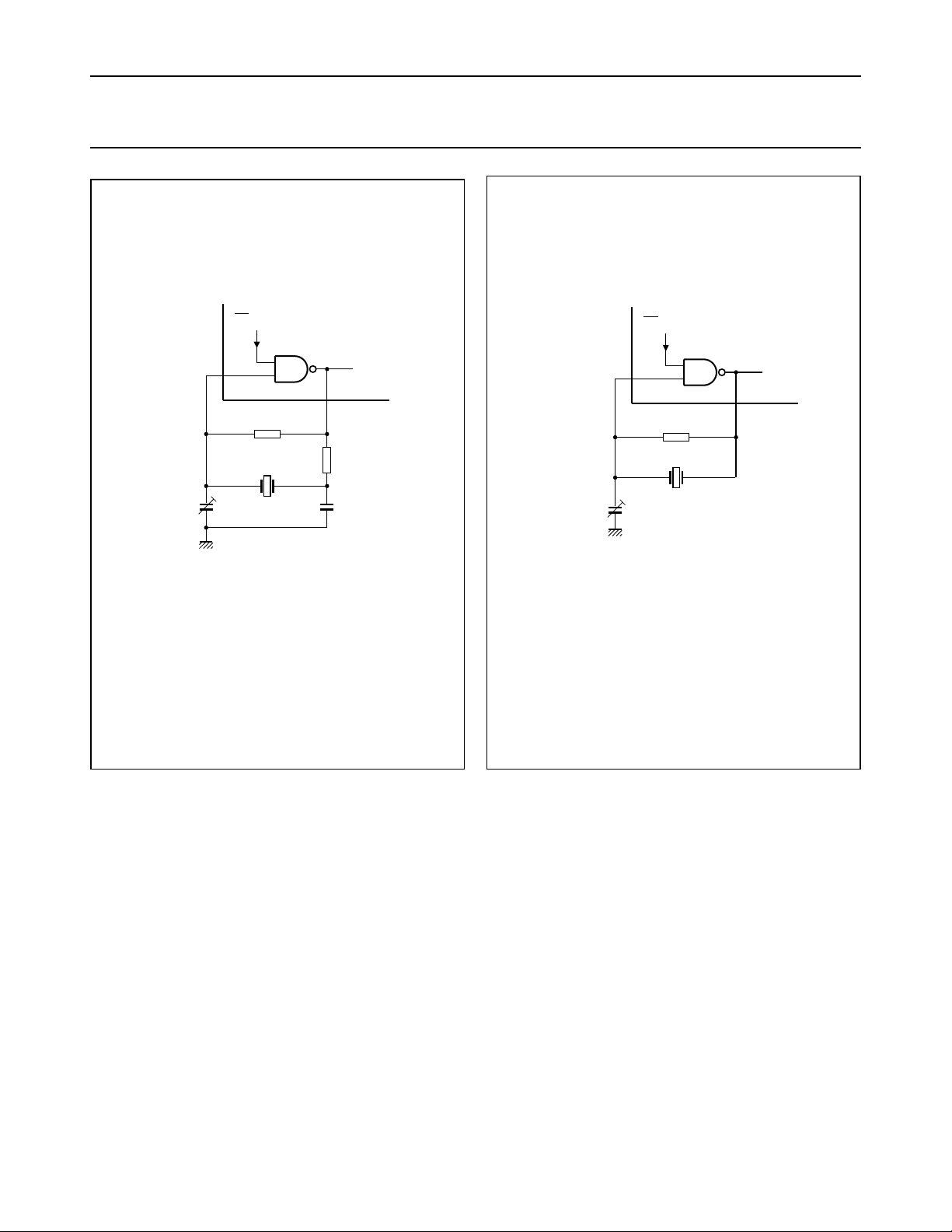
Above 5 MHz replace R2 by a capacitor of
half the value of C2.
at which a crystal is specified (or adjusted)
C
L
equals for this application C1 . C2/C1 + C2.
Fig.13 Typical setup for a crystal oscillator
operating in the fundamental mode
(1 MHz to 25 MHz).
Applicable for third overtone crystals (lower
damping resistance at the third harmonic
frequency) at typical 50 MHz. For lower
frequencies extra load capacitors must be
supplied, or increase bias resistor.
Fig.14 Typical set-up for a crystal oscillator
operating in the third overtone mode without
the use of an inductor.
September 1993 14
Page 15

Philips Semiconductors Product specification
Programmable ripple counter with
oscillator; 3-state
Typical Crystal Oscillator
In Fig.13, R2 is the power limiting
resistor. For starting and maintaining
oscillation a minimum
transconductance is necessary, so
R2 should not be too large. A practical
value for R2 is 2.2 kΩ.
The oscillator has been designed to
operate over a wide frequency
spectrum, for quartz crystals
operating in the fundamental mode
and in the overtone mode. The circuit
is a Pierce type oscillator and requires
a minimum of external components.
There are two on-chip capacitors, X1
and X2, of approximately 7 pF.
Together with the stray and input
capacitance the value becomes 12 pF
for 8-pin SO packages. These values
are convenient and make it possible
to run the oscillator in the third
overtone without external capacitors
applied. If a certain frequency is
chosen, the IC parameters, as
forward transconductance, and the
crystal parameters such as the
motional resistances R1
(fundamental), R3 (third overtone)
and R5 (fifth overtone), are of
paramount importance. Also the
values of the external components as
Rs (series resistance) and the crystal
load capacitances play an important
role. Especially in overtone mode
oscillations, Rb (bias resistance) and
the load capacitance values are very
important.
Considerations for Fundamental
Oscillator:
In the fundamental oscillator mode,
the R
b
the inverter stage, so that it operates
as an amplifier with a phase shift of
approximately 180°. The value must
be high, i.e. 100 kΩ up to 10 MΩ. The
load capacitors C1 and C2, must
have a value that is suitable for the
crystal being used. The crystal is
designed for a certain frequency
having a specific load capacitance.
C1 can be used to trim the oscillation
frequency. The series resistance
reduces the total loop gain. One
function of it is therefore to reduce the
power dissipation in the crystal. R
also suppresses overtone oscillations
and introduces a phase shift over a
broad frequency range. This is of less
concern provided Rs is not too high a
value.
Note
A combination of a small load
capacitor value and a small series
resistance, may cause a third
overtone oscillation.
has only the function of biasing
s
74HC/HCT6323A
Considerations for Third-overtone
Oscillator:
In the overtone configuration, series
resistance is no longer applied. This
is essential otherwise the gain for
third overtone can be too small for
oscillation. A simple solution to
suppress the fundamental oscillation,
is to spoil the crystal fundamental
activity. By dramatically reducing the
value of the bias resistor of the
inverting stage, and applying small
load capacitors, it is possible to have
an insufficient phase in the total loop
for fundamental oscillation. However
the phase for third overtone is good. It
can be explained by the R
constant. During oscillation the
crystal with the load capacitors cause
a phase shift of 180°. Because Rb is
parallel with the crystal (no Rs), R
spoils the phase for fundamental.
Rb× Cl must be of a value, that it is
not spoiling the phase for third
overtone too much. Because third
overtone is a 3 times higher
frequency than the fundamental, the
Rb× Cl cannot 'maintain' the higher
third overtone frequency, which
results in a less spoiled overtone
phase.
PACKAGE OUTLINES
“74HC/HCT/HCU/HCMOS Logic
See
Package Outlines”
.
× Cl time
b
b
September 1993 15
 Loading...