

Page 1

INTEGRATED CIRCUITS
DATA SH EET
For a complete data sheet, please also download:
•The IC06 74HC/HCT/HCU/HCMOS Logic Family Specifications
•The IC06 74HC/HCT/HCU/HCMOS Logic Package Information
•The IC06 74HC/HCT/HCU/HCMOS Logic Package Outlines
74HC/HCT5555
Programmable delay timer with
oscillator
Product specification
File under Integrated Circuits, IC06
September 1993
Page 2

Philips Semiconductors Product specification
Programmable delay timer with oscillator 74HC/HCT5555
FEATURES
• Positive and negative edge
triggered
• Retriggerable or non-retriggerable
• Programmable delay
minimum: 100 ns
maximum: depends on input
frequency and division ratio
• Divide-by range of 2 to 2
24
• Direct reset terminates output
pulse
• Very low power consumption in
triggered start mode
• 3 oscillator operating modes:
– RC oscillator
– Crystal oscillator
– External oscillator
• Device is unaffected by variations
in temperature and VCC when using
an external oscillator
• Automatic power-ON reset
• Schmitt trigger action on both
trigger inputs
• Direct drive for a power transistor
• Low power consumption in active
mode with respect to TTL type
timers
• High precision due to digital timing
• Output capability: 20 mA
• ICC category: MSI.
APPLICATIONS
• Motor control
• Attic fan timers
• Delay circuits
• Automotive applications
• Precision timing
• Domestic appliances.
GENERAL DESCRIPTION
The 74HC/HCT5555 are high-speed
Si-gate CMOS devices and are pin
compatible with low power Schottky
TTL (LSTTL). They are specified in
compliance with JEDEC standard
no. 7A.
• retriggerable/non-retriggerable
monostable
• automatic power-ON reset
• output control logic
• oscillator control logic
• overriding asynchronous master
reset (MR).
The 74HC/HCT5555 are precision
programmable delay timers which
consist of:
• 24-stage binary counter
• integrated oscillator (using external
timing components)
QUICK REFERENCE DATA
GND = 0 V; T
= 25 °C; tr = tf = 6 ns.
amb
SYMBOL PARAMETER CONDITIONS TYP. UNIT
t
PHL/tPLH
C
I
C
PD
propagation delay CL = 15 pF;
A,
B to Q/Q2424ns
MR to Q/
RS to Q/
Q1920ns
Q2628ns
VCC= 5 V
input capacitance 3.5 3.5 pF
power dissipation
notes 1 and 2 23 36 pF
capacitance per buffer
Notes
1. C
is used to determine the dynamic power dissipation (PD in µW):
PD
PD = CPD x V
2
x fi + Σ(CL x V
CC
2
x fo) where:
CC
fi = input frequency in MHz
fo = output frequency in MHz
Σ(CL x V
2
x fo) = sum of outputs.
CC
CL = output load capacitance in pF
VCC = supply voltage in V
2. For HC the condition is VI = GND to V
CC
For HCT the condition is VI= GND to VCC− 1.5 V.
ORDERING INFORMATION
EXTENDED TYPE
NUMBER
PINS PIN POSITION MATERIAL CODE
PACKAGE
74HC/HCT5555N 16 DIL plastic SOT38Z
74HC/HCT5555D 16 SO16 plastic SOT109A
September 1993 2
Page 3

Philips Semiconductors Product specification
Programmable delay timer with oscillator 74HC/HCT5555
PINNING
SYMBOL PIN DESCRIPTION
RS 1 clock input/oscillator pin
R
TC
C
TC
A 4 trigger input (positive-edge
B 5 trigger input (negative-edge
RTR 6 retriggerable/non-retriggerable
RTR/
Q 7 pulse output (active LOW)
GND 8 ground (0 V)
Q 9 pulse output (active HIGH)
S
− S
0
3
OSC CON 14 oscillator control
MR 15 master reset input (active
V
CC
2 external resistor connection
3 external capacitor connection
triggered)
triggered)
input (active HIGH/active LOW)
10, 11,
programmable input
12, 13
HIGH)
16 positive supply voltage
handbook, halfpage
RS
1
R
2
TC
C
3
TC
A
4
B
RTR/
RTR
Q
GND
5555
5
6
7
8
MGA642
Fig.1 Pin configuration.
V
16
CC
MR
15
OSC
14
CON
S
13
3
S
12
2
S
11
1
S
10
0
Q
9
handbook, halfpage
X / Y CTRDIVm
10
1
11
2
12
4
13
8
2
RX
3
CX
14
16G17
1
17
6
4
5
15
R
I = 0
! G
0
Y = 0
15
Y = 15
+
&
1
CT = 0
S
R
Fig.2 IEC logic diagram.
[T]
CT = m R
V16
MGA643
9
7
September 1993 3
Page 4

Philips Semiconductors Product specification
Programmable delay timer with oscillator 74HC/HCT5555
2 3 10 11 12 13
handbook, full pagewidth
1
14
15
4
5
6
RS
OSC
CON
POWER-ON
MR
A
B
RTR/RTR
RESET
R
TC
SSSS
C
012
TC
CP
24 - STAGE COUNTER
CD
MONOSTABLE
CIRCUITRY
3
OUTPUT
STAGE
Q
Q
MGA644
9
7
FUNCTIONAL DESCRIPTION
The oscillator configuration allows the
design of RC or crystal oscillator
circuits. The device can operate from
an external clock signal applied to the
RS input (RTC and CTC must not be
connected). The oscillator frequency
is determined by the external timing
components (RT and CT), within the
frequency range 1 Hz to 4 MHz
(32 kHz to 20 MHz with crystal
oscillator).
In the HCT version the MR input is
TTL compatible but the RS input has
CMOS input switching levels. The RS
input can be driven by TTL input
levels if RS is tied to VCC via a pull-up
resistor.
The counter divides the frequency to
obtain a long pulse duration. The
24-stage is digitally programmed via
the select inputs (S0 to S3). Pin S3 can
also be used to select the test mode,
which is a convenient way of
functionally testing the counter.
The “5555” is triggered on either the
positive-edge, negative-edge or both.
• Trigger pulse applied to input A for
positive-edge triggering
Fig.3 Functional diagram.
• Trigger pulse applied input
B for
negative-edge triggering
• Trigger pulse applied to inputs A
and B (tied together) for both
positive-edge and negative
triggering.
The Schmitt trigger action in the
trigger inputs, transforms slowly
changing input signals into sharply
defined jitter-free output signals and
provides the circuit with excellent
noise immunity.
The OSC CON input is used to select
the oscillator mode, either
continuously running (OSC CON =
HIGH) or triggered start mode (OSC
CON = LOW). The continuously
running mode is selected where a
start-up delay is an undesirable
feature and the triggered start mode
is selected where very low power
consumption is the primary concern.
The start of the programmed time
delay occurs when output Q goes
HIGH (in the triggered start mode, the
previously disabled oscillator will
start-up). After the programmed time
delay, the flip-flop stages are reset
and the output returns to its original
state.
An internal power-on reset is used to
reset all flip-flop stages.
The output pulse can be terminated
by the asynchronous overriding
master reset (MR), this results in all
flip-flop stages being reset. The
output signal is capable of driving a
power transistor. The output time
delay is calculated using the following
formula (minimum time delay is
100 ns):
1
division ratio (s).×
-- f
i
Once triggered, the output width may
be extended by retriggering the
gated, active HIGH-going input A or
the active LOW-going input
B. By
repeating this process, the output
pulse period (Q = HIGH, Q = LOW)
can be made as long as desired. This
mode is selected by RTR/RTR =
HIGH. A LOW on RTR/RTR makes,
once triggered, the outputs (Q, Q)
independent of further transitions of
inputs A and B.
September 1993 4
Page 5

Philips Semiconductors Product specification
Programmable delay timer with oscillator 74HC/HCT5555
Q
Q CP
Q CP
Q CP
Q CP
Q CP
Q CP
Q CP
dbook, full pagewidth
CP
CD
CD
CD
CD
CD
CD
CD
CD
CD
CD
CD
CD
CD
CD
CD
CD
Q
Q CP
Q CP
Q CP
Q CP
Q CP
Q CP
Q CP
CP
CD
CD
CD
CD
CD
CD
CD
CD
Q
Q CP
Q CP
Q CP
Q CP
Q CP
Q CP
Q CP
CP
CP
MGA655
Q
Q
CD
Q
TC
2
3
S
CON
S
RS
RTCC
OSC
0
1
S
S
September 1993 5
Fig.4 Logic diagram.
CC
V
MR
RTR
A
RTR/
B
Page 6

Philips Semiconductors Product specification
Programmable delay timer with oscillator 74HC/HCT5555
TEST MODE
Set S3 to a logic LOW level, this will divide the 24 stage counter into three, parallel clocking, 8-stage counters. Set S0,
S1 and S2 to a logic HIGH level, this programs the counter to divide-by 28 (256). Apply a trigger pulse and clock in 255
pulses, this sets all flip-flop stages to a logic HIGH level. Set S3 to a logic HIGH level, this causes the counter to divide-by
224. Clock one more pulse into the RS input, this causes a logic 0 to ripple through the counter and output Q/Q goes from
HIGH-to-LOW level. This method of testing the delay counter is faster than clocking in 224 (16 777 216) clock pulses.
FUNCTION TABLE
INPUTS OUTPUTS
MR A
HXXLH
L↑X one HIGH level
LX↓one HIGH level
Notes
1. H = HIGH voltage level
L = LOW voltage level
X = don't care
↑ = LOW-to-HIGH transition
↓ = HIGH-to-LOW transition.
BQQ
one LOW level
output pulse
output pulse
output pulse
one LOW level
output pulse
September 1993 6
Page 7
Philips Semiconductors Product specification
Programmable delay timer with oscillator 74HC/HCT5555
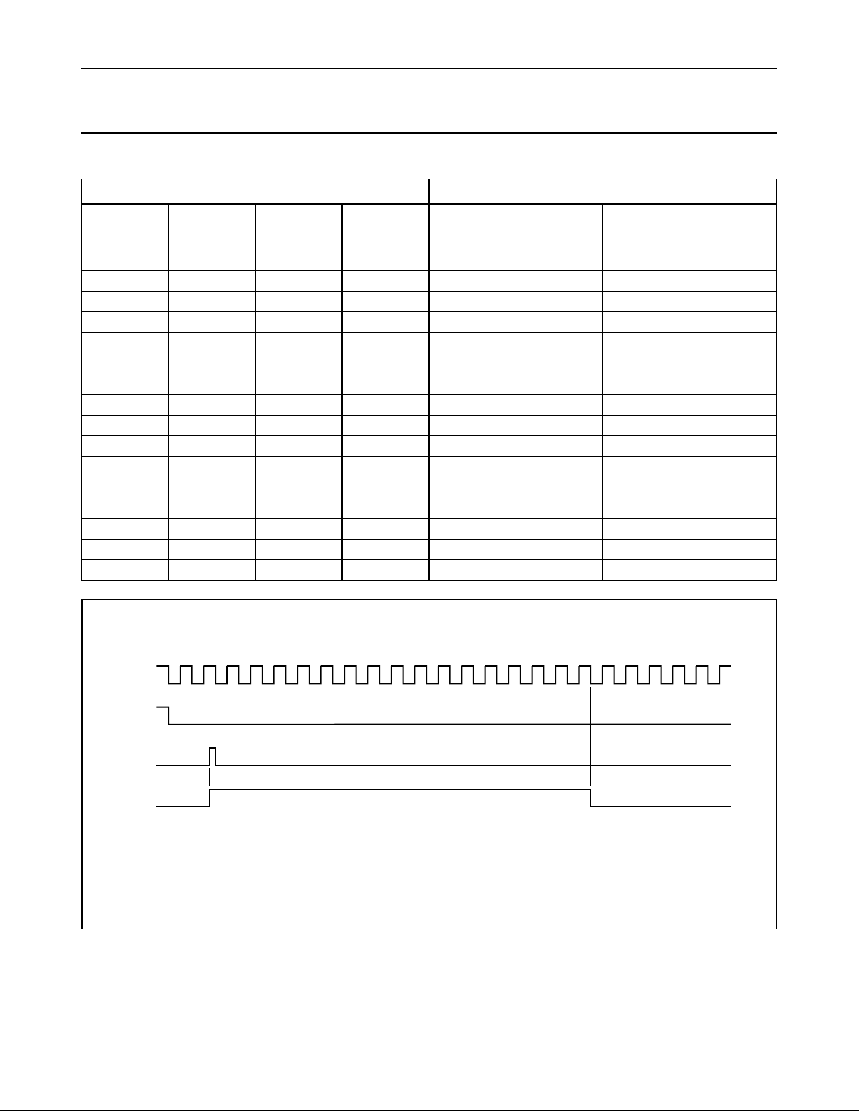
DELAY TIME SELECTION
SELECT INPUTS OUTPUT Q/Q (FREQUENCY DIVIDING)
S
3
LLLL2
LLLH2
LLHL2
LLHH2
LHLL2
LHLH2
LHHL2
LHHH2
S
2
S
1
S
0
1
2
3
4
5
6
7
8
BINARY DECIMAL
2
4
8
16
32
64
128
256
..... .
HLLL2
HLLH2
HLHL2
HLHH2
HHLL2
HHLH2
HHHL2
HHHH2
17
18
19
20
21
22
23
24
131 072
262 144
524 288
1 048 576
2 097 152
4 194 304
8 388 608
16 777 216
1 2 3 4 5 6 7 8 9 10 11 12 13 14 15 16
handbook, full pagewidth
RS
MR
A
Q
Timing example shown for S3, S2, S1, S0 = 0011 (binary 24, decimal 16).
Fig.5 Timing diagram.
September 1993 7
MGA649
Page 8
Philips Semiconductors Product specification
Programmable delay timer with oscillator 74HC/HCT5555
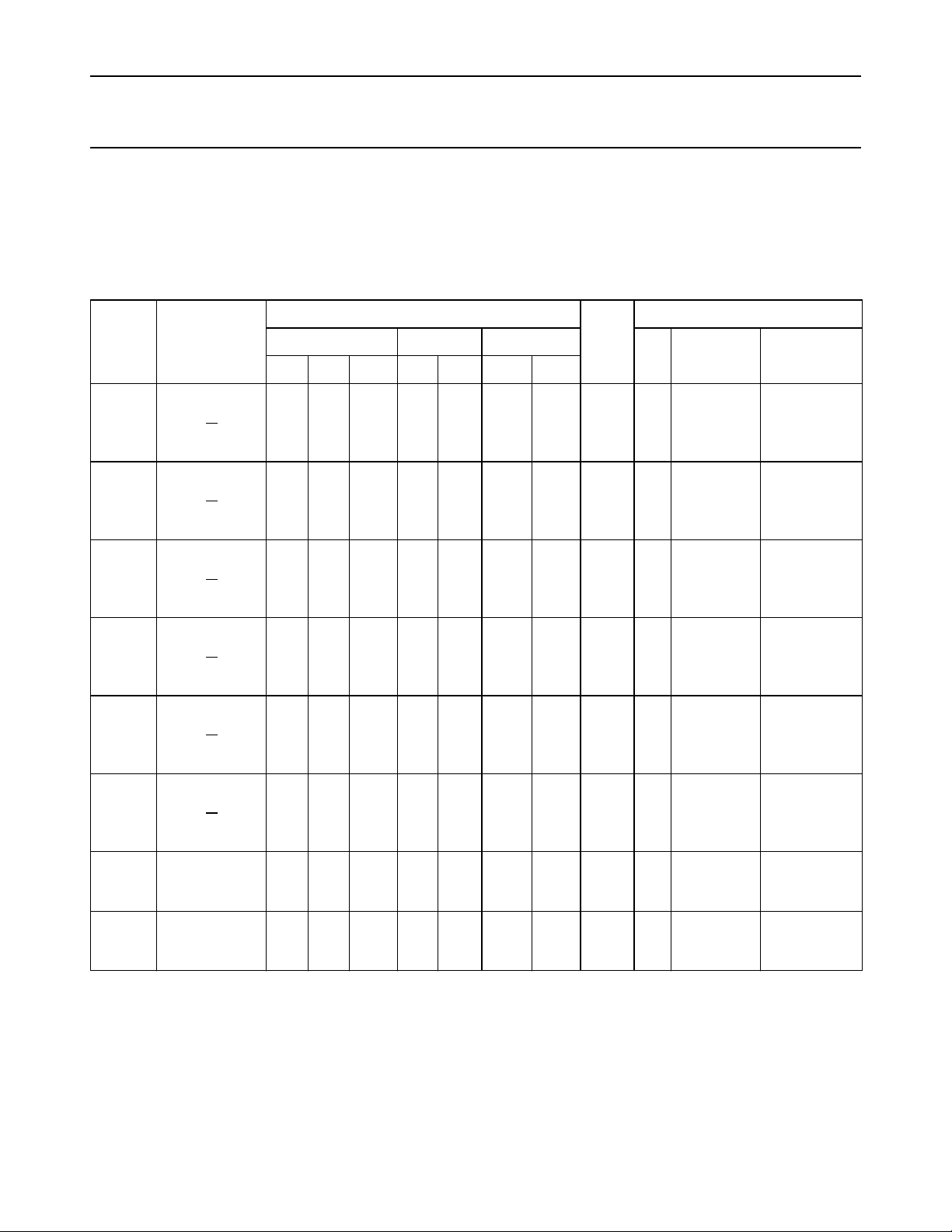
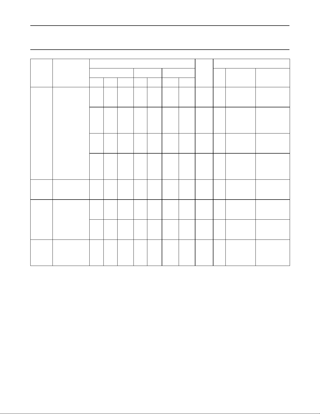
DC CHARACTERISTICS FOR 74HC
For the DC characteristics see
“74HC/HCT/HCU/HCMOS Logic Family Specifications”
Output capability: parallel outputs, bus driver; serial output, standard ICC category: MSI.
DC CHARACTERISTICS FOR 74HC
(°C)
T
amb
SYM-
BOL
V
OH
PARAMETER
HIGH level
output voltage
Q and Q
+25 −40 to +85 −40 to +125
MIN TYP MAX MIN MAX MIN MAX
1.9
2
4.4
5.9
4.5
6.0
−
−
−
1.9
4.4
5.9
−
1.9
−
4.4
−
5.9
−
−
−
UNIT
V
V
V
V
(V)
2.0
4.5
6.0
outputs
V
OH
HIGH level
output voltage
3.98
5.48
4.32
5.81−−
3.84
5.34−−
3.7
5.2−−
V
V
4.5
6.0
Q and Q
outputs
V
OH
HIGH level
output voltage
3.3
4.8−−
−
−
3
4.5−−
2.7
4.2−−
V
V
4.5
6.0
Q and Q
outputs
V
OL
LOW level
output voltage
Q and Q
−
0
0.1
−
0
0.1
−
0
0.1
−
0.1
−
−
0.1
−
−
0.1
−
0.1
0.1
0.1
V
V
V
2.0
4.5
6.0
outputs
V
OL
LOW level
output voltage
−
0.15
0.26
−
0.15
0.26−−
0.33
0.33−−
0.40
0.40VV
4.5
6.0
Q and Q
outputs
V
OL
LOW level
output voltage
−
−
0.9
−
−
0.9−−
1.14
1.14−−
1.34
1.34VV
4.5
6.0
Q and Q
outputs
V
IH
V
IL
HIGH level
input voltage
RS input
LOW level
input voltage
RS input
1.7
3.6
4.8
−
−
−
−
−
−
−
−
−
−
0.3
−
0.9
−
1.2
1.7
3.6
4.8
−
−
−
−
−
−
0.3
0.9
1.2
1.7
3.6
4.8
−
−
−
−
−
−
0.3
0.9
1.2
V
V
V
V
V
V
2
4.5
6.0
2.0
4.5
6.0
.
TEST CONDITION
CC
V
I
OTHER
Io = −20 µA
Io = −6.0 mA
Io = −7.8 mA
Io = −20 mA
Io = −20 mA
Io = 20 µA
Io = 6.0 mA
Io= 7.8 mA
Io = 20 mA
Io = 25 mA
September 1993 8
Page 9
Philips Semiconductors Product specification
Programmable delay timer with oscillator 74HC/HCT5555
T
SYM-
BOL
V
OH
V
OH
V
OL
V
OL
PARAMETER
HIGH level
output voltage
RTC output
HIGH level
output voltage
CTC output
LOW level
output voltage
RTC output
LOW level
output voltage
CTC output
(°C)
amb
+25 −40 to +85 −40 to +125
MIN TYP MAX MIN MAX MIN MAX
3.98
5.48−−
3.98
5.48−−
1.9
4.4
5.9
1.9
4.4
5.9
3.98
5.48−−
−
−
−
−
−
−
−
2.0
4.5
6
2.0
4.5
6.0
−
−
0
0
0
−
−
−
−
−
−
−
−
−
−
−
−
−
−
0.26
0.26−−
0.1
0.1
0.1
0.26
0.26−−
3.84
5.34−−
3.84
5.34−−
1.9
4.4
5.9
1.9
4.4
5.9
3.84
5.34−−
−
−
−
−
−
−
−
−
−
0.33
0.33−−
0.1
0.1
0.1
0.33
0.33−−
3.7
5.2−−
3.7
5.2−−
1.9
4.4
5.9
1.9
4.4
5.9
3.7
5.2−−
−
−
−
−
−
−
−
−
−
0.4
0.4VV
0.1
0.1
0.1
0.4
0.4VV
UNIT
V
V
V
V
V
V
V
V
V
V
V
V
V
V
V
TEST CONDITION
V
CC
(V)
4.5
6.0
4.5
6.0
V
I
RS = GND;
OSC CON
= V
CC
RS = V
CC
OSC CON
= GND;
untriggered
2.0
4.5
6.0
2
4.5
6.0
RS = V
OSC CON
= V
RS = V
OSC CON
= GND;
CC
CC
CC
untriggered
4.5
RS = VIH;
6.0
OSC CON
= V
IH
4.56RS = VCC;
OSC CON
= V
CC
2.0
4.5
6
4.5
6.0
RS = V
OSC CON
= V
RS = VIL;
OSC CON
CC
CC
= VIL;
untriggered
OTHER
Io = −2.6 mA
Io = −3.3 mA
;
Io = −0.65 mA
Io = −0.85 mA
;
Io = −20 µA
;
Io = −20 µA
Io = −3.2 mA
Io = −4.2 mA
Io = 2.6 mA I
= 3.3 mA
;
Io = 20 µA
Io = 3.2 mA I
= 4.2 mA
o
o
September 1993 9
Page 10
Philips Semiconductors Product specification
Programmable delay timer with oscillator 74HC/HCT5555
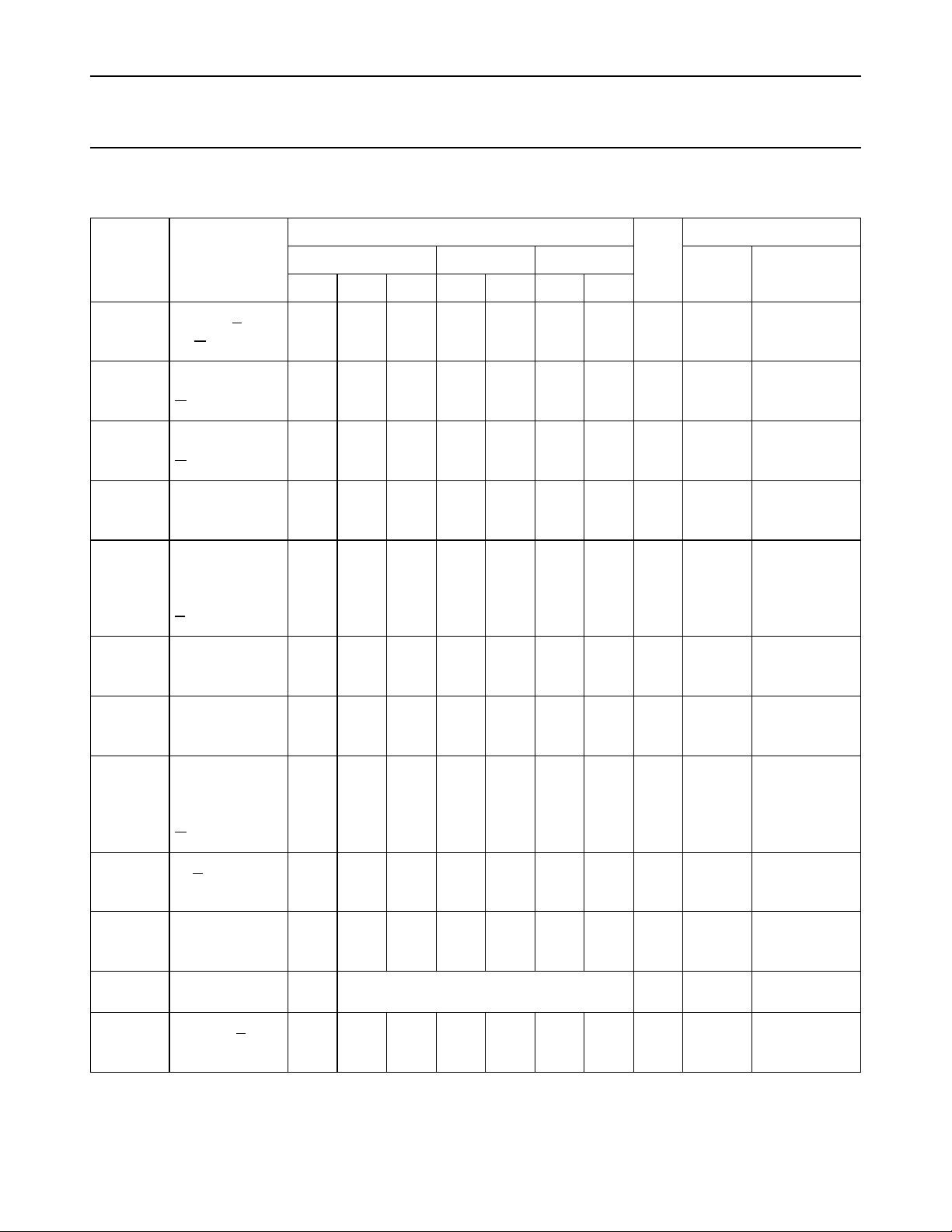
AC CHARACTERISTICS FOR 74HC
GND = 0 V; t
= tf = 6 ns; CL = 50 pF.
r
SYMBOL PARAMETER
t
PLH/tPHL
propagation
delay A, B to
Q, Q
t
PLH/tPHL
propagation
delay MR to Q,
Q
t
PLH/tPHL
propagation
delay RS to Q,
Q
t
THL/tTLH
output
transition time−−
t
W
trigger pulse
width
A = HIGH
B = LOW
t
W
master reset
pulse width
HIGH
t
W
clock pulse
width RS;
HIGH or LOW
t
W
minimum
output pulse
width
Q = HIGH,
Q = LOW
t
rt
retrigger time
A, B
R
EXT
external timing
resistor
C
EXT
external timing
capacitor
t
rem
removal time
MR to A, B
(°C)
T
amb
+25 −40 to +85 −40 to +125
MIN TYP MAX MIN MAX MIN MAX
−
−
−
−
−
−
−
−
−
−
70
14
12
70
14
12
80
16
14
−
−
−
−
−
−
5
1
50
50
120
24
20
77
28
22
61
22
18
83
30
24
19
7
6
17
6
5
19
7
6
25
9
7
275
100
80
0
0
0
−
−
39
14
11
240
48
41
185
37
31
250
50
43
75
15
13
−
−
−
−
−
−
−
−
−
−
−
−
−
−
−
1000
1000−−
−
−
−
−
−
−
−
−
−
−
−
−
−
−
−
90
18
15
90
18
15
100
20
17
−
−
−
−
−
−
no limits
150
30
26
300
60
51
230
46
39
315
63
54
95
19
16
−
−
−
−
−
−
−
−
−
−
−
−
−
−
−
105
21
18
− 105
21
18
−
−
−
−
−
−
−
−
−
−
−
120
24
20
−
−
−
−
−
−
−
−
−
−
−
−
180
36
31
360
72
61
280
56
48
375
75
64
110
22
19
−
−
−
−
−
−
−
−
−
−
−
−
−
−
−
−
−
−
−
−
−
UNIT
ns
ns
ns
ns
ns
ns
ns
ns
ns
ns
ns
ns
ns
ns
ns
ns
ns
ns
ns
ns
ns
ns
ns
ns
ns
ns
ns
2.0
4.5
6.0
2.0
4.5
6.0
2.0
4.5
6.0
2.0
4.5
6.0
2.0
4.5
6.0
2.0
4.5
6.0
2.0
4.5
6.0
2.0
4.5
6.0
2.0
4.5
6.0
kΩkΩ2.0
5.0
pF
pF
ns
ns
ns
2.0
5.0
2.0
4.5
6.0
TEST CONDITION
V
CC
(V)
WAVEFORMS
Fig.6
Fig.7
Fig.8; note 1
Fig.6
Fig.6
Fig.7
Fig.8
Fig.6; note 1
Fig.10; note 2
Fig.13
Fig.13
Fig.7
September 1993 10
Page 11
Philips Semiconductors Product specification
Programmable delay timer with oscillator 74HC/HCT5555
T
(°C)
amb
SYMBOL PARAMETER
+25 −40 to +85 −40 to +125
UNIT
MIN TYP MAX MIN MAX MIN MAX
f
f
max
max
maximum
clock pulse
frequency
maximum
clock pulse
frequency
2
10
12
6
30
35
5.9
18
21
24.8
75
89
−
−
−
−
−
−
1.8
8
10
4.8
24
28
−
−
−
−
−
−
1.3
6.6
8
4
20
24
−
−
−
−
−
−
MHz
MHz
MHz
MHz
MHz
MHz
Notes
1. One stage selected.
2. It is possible to retrigger directly after the trigger pulse, however the pulse will only be extended, if the time period
exceeds the clock input cycle time divided by 2.
3. One stage selected. The termination of the output pulse remains synchronized with respect to the falling edge of the
RS clock input.
4. One stage selected. The termination of the output pulse is no longer synchronized with respect to the falling edge of
the RS clock input.
TEST CONDITION
V
CC
(V)
2.0
WAVEFORMS
Fig.8; note 3
4.5
6.0
2.0
Fig.9; note 4
4.5
6.0
September 1993 11
Page 12
Philips Semiconductors Product specification
Programmable delay timer with oscillator 74HC/HCT5555
DC CHARACTERISTICS FOR 74HCT
For the DC characteristics see
“74HC/HCT/HCU/HCMOS Logic Family Specifications”
Output capability: non-standard; bus driver with extended specification on VOH and V
ICC category: MSI.
.
OL
SYMBOL PARAMETER
V
OH
HIGH level
output voltage
Q and Q
outputs
V
OH
HIGH level
output voltage
Q and Q
outputs
V
OH
HIGH level
output voltage
Q and Q
outputs
V
OL
LOW level
output voltage
Q and Q
outputs
V
OL
LOW level
output voltage
Q and Q
outputs
V
OL
LOW level
output voltage
Q and Q
outputs
(°C)
T
amb
+25 −40 to +85 −0to+125
MIN TYP MAX MIN MAX MIN MAX
UNIT
TEST CONDITION
V
CC
(V)
V
I
OTHER
4.4 4.5 − 4.4 − 4.4 − V 4.5 Io = −20 µA
3.98 4.32 − 3.84 − 3.7 − V 4.5 Io = −6 mA
3.3 −− 3− 2.7 − V 4.5 Io = −20 mA
− 0 0.1 − 0.1 − 0.1 V 4.5 Io = 20 µA
− 0.15 0.26 − 0.33 − 0.40 V 4.5 Io = 6 mA
−−0.9 − 1.14 − 1.34 V 4.5 − Io = 20 mA
September 1993 12
Page 13
Philips Semiconductors Product specification
Programmable delay timer with oscillator 74HC/HCT5555
T
SYMBOL PARAMETER
V
OH
HIGH level
output
voltage R
TC
output
HIGH level
OH
output
voltage C
TC
V
output
LOW level
OL
output
voltage R
TC
V
output
LOW level
OL
output
voltage C
TC
V
output
(°C)
amb
+25 −40 to +85 −0to+125
UNIT
MIN TYP MAX MIN MAX MIN MAX
3.98 −− 3.84 − 3.7 − V 4.5 RS = GND;
3.98 −− 3.84 − 3.7 − V 4.5 RS = V
4.4 4.5 − 4.4 − 4.4 − V 4.5 RS = V
4.4 4.5 − 4.4 − 4.4 − V 4.5 RS = V
3.98 −− 3.84 − 3.7 − V 4.5
−−0.26 − 0.33 − 0.4 V 4.5
− 0 0.1 − 0.1 − 0.1 V 4.5
−−0.26 − 0.33 − 0.4 V 4.5
TEST CONDITION
V
CC
(V)
OSC CON
=V
CC
OSC CON
= GND;
untriggered
OSC CON
= V
CC
OSC CON
= GND;
untriggered
RS = VIH;
OSC CON
= V
IH
RS = V
OSC CON
= V
CC
RS = V
OSC CON
= V
CC
RS = VIL;
OSC CON
= VIL;
untriggered
V
I
OTHER
Io = −2.6 mA
;
Io =
CC
−0.65 mA
;
Io = −20 µA
CC
;
Io = −20 µA
CC
Io = −3.2 mA
;
CC
Io = 2.6 mA
;
CC
Io = 20 µA
Io = 3.2 mA
Notes
1. The RS input has CMOS input switching levels.
2. The value of additional quiescent supply current (∆ICC) for a unit load of 1 is given in the family specifications. To
determine ∆ICC per input, multiply this value by the unit load coefficient shown in the following table.
UNIT LOAD COEFFICIENT
INPUT UNIT LOAD COEFFICIENT
MR 0.35
A 0.69
B 0.50
RTR/
RTR 0.35
OSC CON 1.20
S0 - S
S
3
2
0.65
0.40
September 1993 13
Page 14
Philips Semiconductors Product specification
Programmable delay timer with oscillator 74HC/HCT5555
AC CHARACTERISTICS FOR 74HCT
GND = 0 V; t
= tf = 6 ns; CL = 50 pF.
r
SYMBOL PARAMETER
t
PLH/tPHL
propagation
delay A, B to
Q, Q
t
PHL/tPLH
propagation
delay MR to Q,
Q
t
PHL/tPLH
propagation
delay RS to Q,
Q
t
THL/tTLH
output
transition time
t
W
trigger pulse
width
A = HIGH
B = LOW
t
W
master reset
pulse width
HIGH
t
W
clock pulse
width RS;
HIGH or LOW
t
W
minimum
output pulse
width
Q = HIGH,
Q = LOW
t
rt
retrigger time
A, B
R
EXT
external timing
resistor
C
EXT
external timing
capacitor
t
rem
removal time
MR to A, B
f
max
maximum
clock pulse
frequency
f
max
maximum
clock pulse
frequency
(°C)
T
amb
+25 −40 to +85 −40 to +125
MIN TYP MAX MIN MAX MIN MAX
UNIT
TEST CONDITION
V
CC
(V)
WAVEFORMS
− 28 48 − 60 − 72 ns 4.5 Fig.6
− 24 41 − 51 − 62 ns 4.5 Fig.7
− 32 54 − 68 − 81 ns 4.5 Fig.8; note 1
− 715−19 − 22 ns 4.5 Fig.6
21 12 − 26 − 32 − ns 4.5 Fig.6
14 5 − 18 − 21 − ns 4.5 Fig.7
16 9 − 20 − 24 − ns 4.5 Fig.8
− 100 −−−−−ns 4.5 Fig.6
− 0 −−−−−ns 4.5 Fig.10; note 2
1 − 1000 −−−−kΩ4.5 Fig.13
50 no limits pF 4.5 Fig.13
24 14 − 30 − 36 − ns 4.5 Fig.7
10 18 − 8 − 6.6 − MHz 4.5 Fig.8; note 3
30 75 − 24 − 20 − MHz 4.5 Fig.9; note 4
September 1993 14
Page 15

Philips Semiconductors Product specification
Programmable delay timer with oscillator 74HC/HCT5555
Notes
1. One stage selected.
2. It is possible to retrigger directly after the trigger pulse, however the pulse will only be extended, if the time period
exceeds the clock input cycle time divided by 2.
3. One stage selected. The termination of the output pulse remains synchronized with respect to the falling edge of the
RS clock input.
4. One stage selected. The termination of the output pulse is no longer synchronized with respect to the falling edge of
the RS clock input.
September 1993 15
Page 16
Philips Semiconductors Product specification
Programmable delay timer with oscillator 74HC/HCT5555
AC WAVEFORMS
t
handbook, full pagewidth
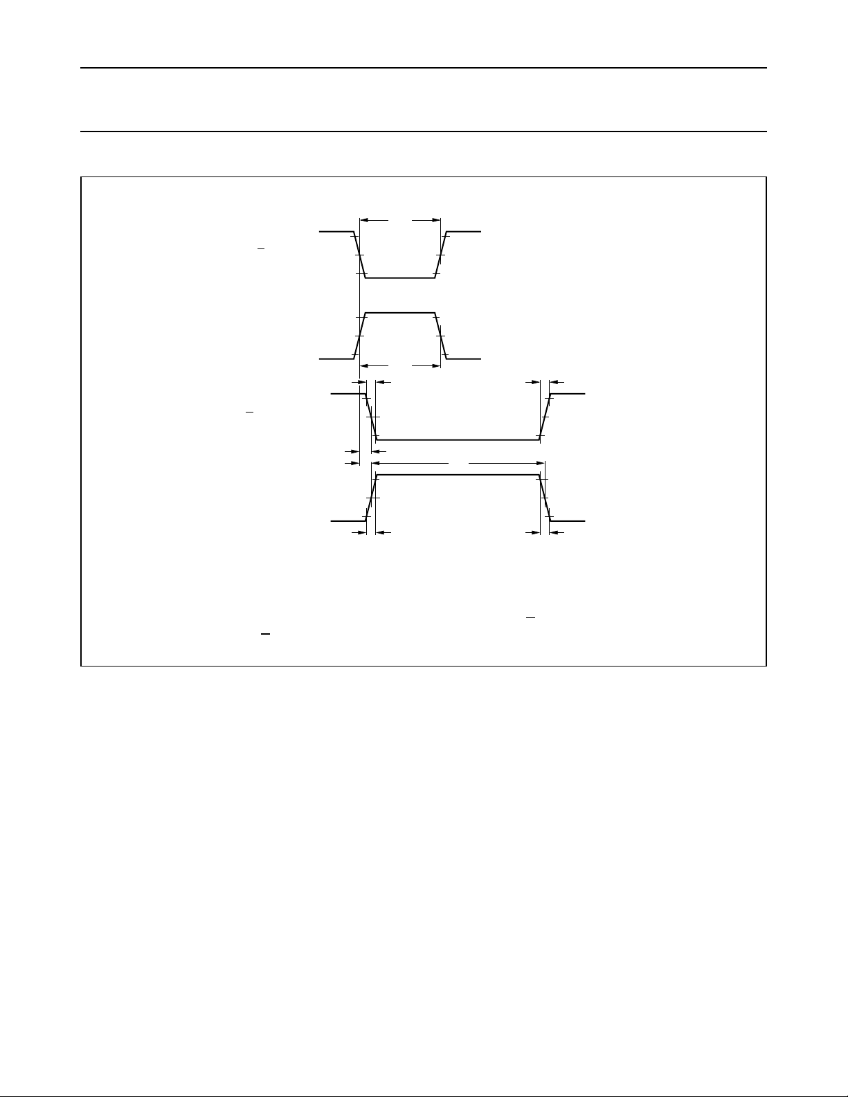
(1) HC : VM= 50%; VI= GND to VCC.
= 1.3 V; VI= GND to 3 V.
HCT: V
M
B INPUT
A INPUT
Q OUTPUT
Q OUTPUT
GND
t
t
90%
10%
90%
10%
PHL
PLH
W
(1)
V
M
(1)
V
M
t
W
t
THL
(1)
V
M
t
W
(1)
V
M
t
TLH
t
TLH
t
90%
10%
90%
10%
THL
MGA653
Fig.6 Waveforms showing the triggering of the delay timer by input A or B, the minimum pulse widths of the
trigger inputs A and B, the output pulse width and output transition times.
September 1993 16
Page 17
Philips Semiconductors Product specification
Programmable delay timer with oscillator 74HC/HCT5555
handbook, full pagewidth
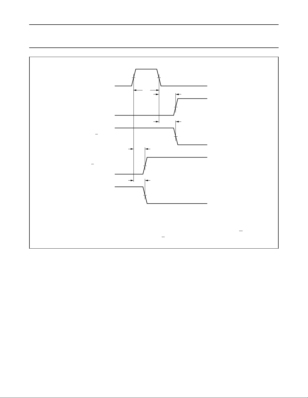
(1) HC : VM= 50%; VI= GND to VCC.
= 1.3 V; VI= GND to 3 V.
HCT: V
M
MR INPUT
A INPUT
B INPUT
Q OUTPUT
Q OUTPUT
V
t
PLH
t
PHL
(1)
M
t
W
V
V
t
rem
(1)
V
M
t
rem
(1)
V
M
(1)
M
(1)
M
MGA652-1
Fig.7 Waveforms showing the master reset (MR) pulse width, the master reset to outputs (Q and Q) propagation
delays and the master reset to trigger inputs (A and B) removal time.
September 1993 17
Page 18
Philips Semiconductors Product specification
Programmable delay timer with oscillator 74HC/HCT5555
handbook, full pagewidth
RS INPUT
Q OUTPUT
Q OUTPUT
(1) HC : VM= 50%; VI= GND to VCC.
= 1.3 V; VI= GND to 3 V.
HCT: V
M
1
t
t
V
2
PHL
PLH
CC
1/f max
(1)
V
M
(1)
V
M
t
W
MGA651
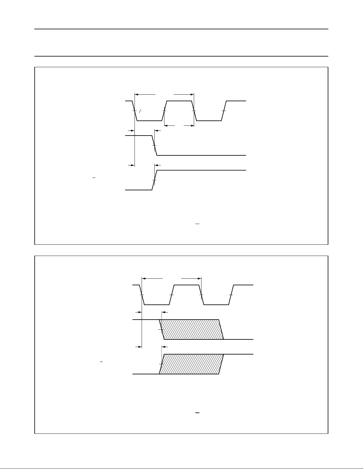
Fig.8 Waveforms showing the clock (RS) to outputs (Q and Q) propagation delays, the clock pulse width and
the maximum clock frequency.
M
PHL
V
PLH
V
1/f max
(1)
(1)
M
(1)
M
MGA654
handbook, full pagewidth
(1) HC : VM= 50%; VI= GND to VCC.
= 1.3 V; VI= GND to 3 V.
HCT: V
M
RS INPUT
Q OUTPUT
Q OUTPUT
V
t
t
Fig.9 Waveforms showing the clock (RS) to outputs (Q and Q) propagation delays, the clock pulse width and
the maximum clock frequency (Output waveforms are not synchronized with respect to the RS waveform).
September 1993 18
Page 19
Philips Semiconductors Product specification
Programmable delay timer with oscillator 74HC/HCT5555
handbook, full pagewidth
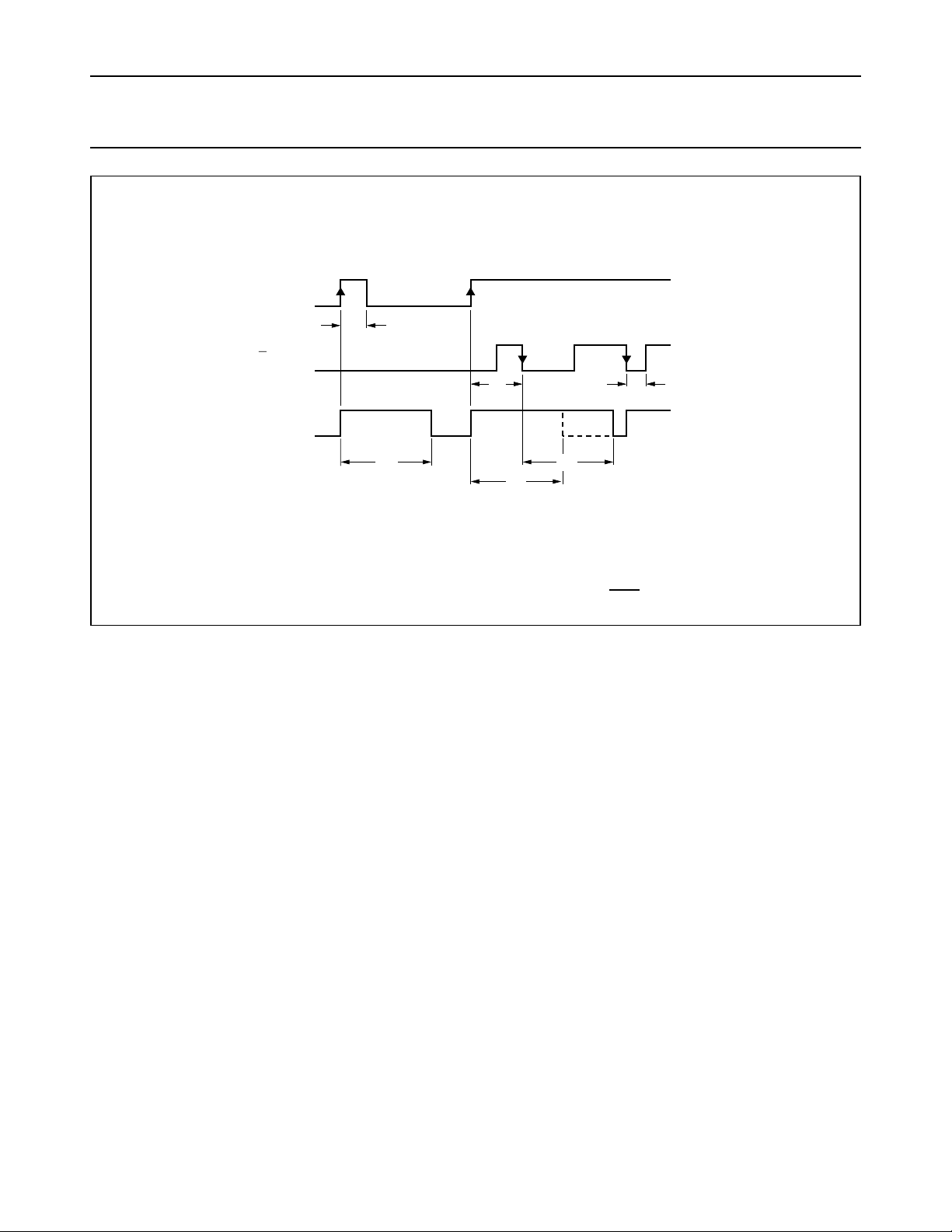
(1) HC : VM= 50%; VI= GND to VCC.
= 1.3 V; VI= GND to 3 V.
HCT: V
M
Fig.10 Output pulse control using retrigger pulse (RTR/RTR = HIGH).
A INPUT
B INPUT
Q OUTPUT
t
W
t
rt
t
W
t
W
t
W
t
W
MGA650
September 1993 19
Page 20
Philips Semiconductors Product specification
Programmable delay timer with oscillator 74HC/HCT5555
APPLICATION INFORMATION
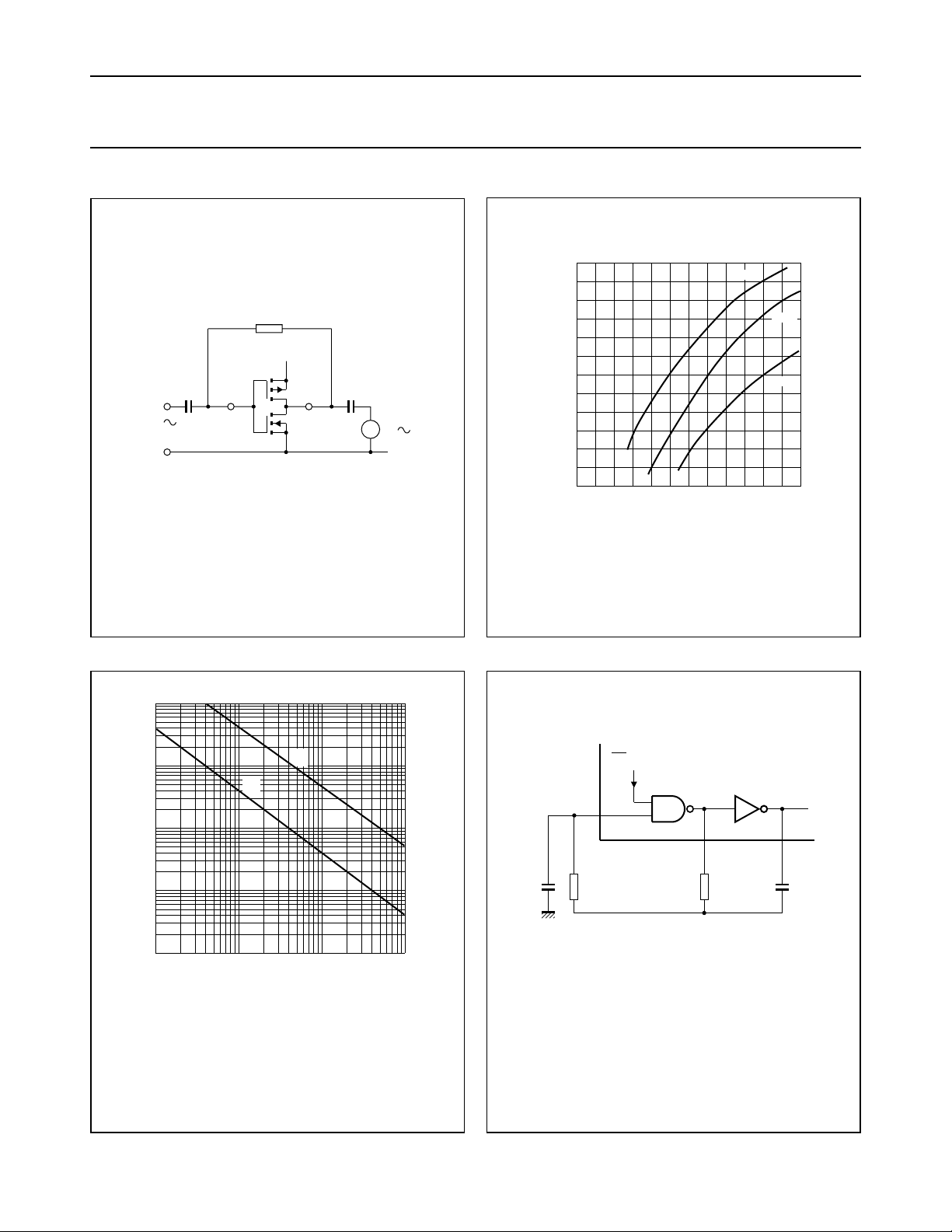
R = 560 kΩ
input
bias
V
CC
output
handbook, halfpage
v
i
(f = 1 kHz)
0.47 F
µ
Fig.11 Test set-up for measuring forward
transconductance gfs = dio/dvi at vo is
constant (see Fig.12) and MR = LOW.
5
10
handbook, halfpage
f
osc
(Hz)
4
10
C
3
10
R
t
t
100 F
MGA645
µ
i
A
o
MGA647
GND
g
fs
(mA/V)
14
12
10
handbook, halfpage
8
6
4
2
0123456
max.
V
CC
MBA333
typ.
min.
(V)
Fig.12 Typical forward transconductance gfs as a
function of the supply voltage at VCC at
T
= 25 °C.
amb
handbook, halfpage
MR (from logic)
RS1
R
TC
2
C
TC
3
2
10
10
3
10
–4
10
Ct curve at Rt = 100 kΩ; R2 = 200 kΩ.
Rt curve at Ct = 1 nF; R2 = 2 x Rt.
RC oscillator frequency as a function of Rt and C
at VCC = 2 to 6 V; T
amb
4
10
–3
10
= 25 °C.
5
R ( )
10
–2
10
C ( F)
t
t
6
10
Ω
t
–1
10
µ
Fig.13 Application information.
September 1993 20
C2 R2
R
t
MGA646
Typical formula for oscillator frequency:
=
--------------------------------
2.5 RtCt××
1
f
osc
Fig.14 Example of an RC oscillator.
C
t
Page 21

Philips Semiconductors Product specification
Programmable delay timer with oscillator 74HC/HCT5555
Timing Component Limitations
The oscillator frequency is mainly
determined by RtCt, provided R2 ≈
2Rt and R2C2 << RtCt. The function
of R2 is to minimize the influence of
the forward voltage across the input
protection diodes on the frequency.
The stray capacitance C2 should be
kept as small as possible. In
consideration of accuracy, Ct must be
larger than the inherent stray
capacitance. Rt must be larger than
the “ON” resistance in series with it,
which typically is 280 Ω at
VCC= 2 V, 130 Ω at VCC = 4.5 V and
100 Ω at VCC = 6 V. The
recommended values for these
components to maintain agreement
with the typical oscillation formula are:
Ct> 50 pF, up to any practical value,
10 kΩ< Rt< 1 MΩ.
In order to avoid start-up problems,
Rt>> 1 kΩ.
Typical Crystal Oscillator
In Fig.15, R2 is the power limiting
resistor. For starting and maintaining
oscillation a minimum
transconductance is necessary, so
R2 should not be too large. A practical
value for R2 is 2.2 kΩ. Above 14 MHz
it is recommended replacement of R2
by a capacitor with a typical value of
35 pF.
Accuracy
Device accuracy is very precise for
long time delays and has an accuracy
of better than 1% for short time delays
(1% applies to values ≥ 400 ns).
Tolerances are dependent on the
external components used, either RC
network or crystal oscillator.
Start-up Using External Clock
The start of the timing pulse is
initiated directly by the trigger pulse
(asynchronously with respect to the
oscillator clock). Triggering on a clock
HIGH or clock LOW results in the
following:
• clock = HIGH; the timing pulse may
be lengthened by a maximum of
tW/2 (tW = clock pulse width)
• clock = LOW; the timing pulse may
be shortened by a maximum of tW/2
(tW = clock pulse width).
This effect can be minimized by
selecting more delay stages. When
using only one or two delay stages, it
is recommended to use an external
time base that is synchronized with
the negative-edge of the clock.
Start-up Using RC Oscillator
The first clock cycle is ≈35% of a time
period too long. This effect can also
be minimized by selecting more delay
stages.
Start-up Using Crystal Oscillator
A crystal oscillator requires at least
two clock cycles to start-up plus an
unspecified period (ms) before the
amplitude of the clock signal
increases to its expected level.
Although this device also operates at
lower clock amplitudes, it is
recommended to select the
continuously running mode
(OSC CON = HIGH) to prevent
start-up delays.
Termination of the Timing Pulse
The end of the timing pulse is
synchronized with the falling edge of
the oscillator clock. The timing pulse
may lose synchronization under the
following conditions:
• high clock frequency and large
number of stages are selected.
This depends on the dynamic
relationship that exists between the
clock frequency and the ripple
through delay of the subsequent
stages.
Synchronization
When frequencies higher than those
specified in the Table
'Synchronization limits' are used, the
termination of timing pulse will lose
synchronization with the falling edge
of the oscillator. The unsynchronized
timing pulse introduces errors, which
can be minimized by increasing the
number of stages used e.g. a 20 MHz
clock frequency using all 24 stages
will result in a frequency division of
16 777 225 instead of 16 777 216, an
error of 0.0005%.
The amount of error increases at high
clock frequencies as the number of
stages decrease. A clock frequency
of 40 MHz and 4 stages selected
results in a division of 18 instead of
16, a 12.5% error. Application
example:
• If a 400 ns timing pulse was
required it would be more accurate
to utilize a 5 MHz clock frequency
using 1 stage or a 10 MHz clock
frequency using 2 stages (due to
synchronization with falling edge of
the oscillator) than a 40 MHz clock
frequency and 4 stages
(synchronization is lost).
September 1993 21
Page 22
Philips Semiconductors Product specification
Programmable delay timer with oscillator 74HC/HCT5555
Minimum Output Pulse Width
The minimum output pulse width is
determined by the minimum clock
pulse width, plus the maximum
propagation delay of A, B to Q. The
rising edge of Q is dominated by the
A,B to Q propagation delay, while the
falling edge of Q is dominated by RS
to Q propagation delay. These
propagation delays are not equal. The
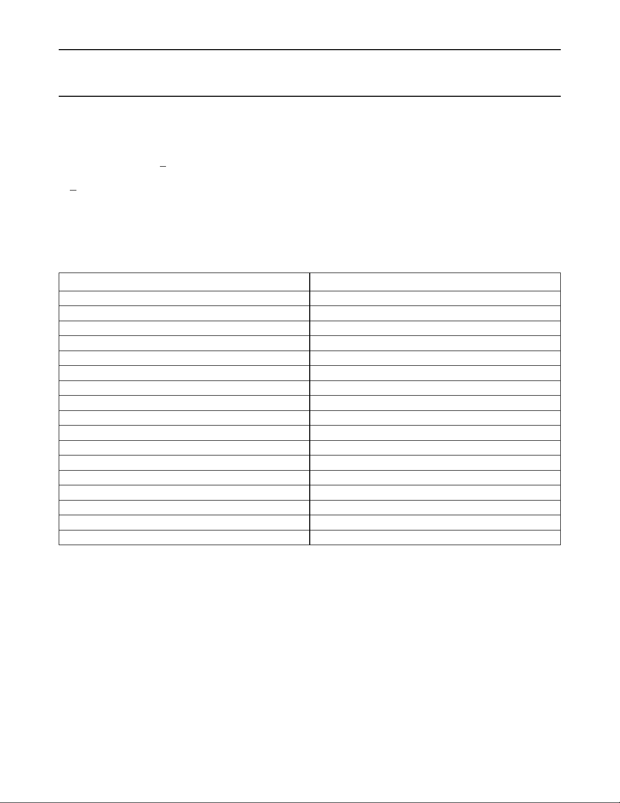
SYNCHRONIZATION LIMITS
NUMBER OF STAGES SELECTED CLOCK FREQUENCY (TYPICAL)
1 18 MHz
2 14 MHz
3 11 MHz
4 9.6 MHz
5 8.3 MHz
6 7.3 MHz
7 6.6 MHz
8 6 MHz
..
17 3.2 MHz
18 3.0 MHz
19 2.9 MHz
20 2.8 MHz
21 2.7 MHz
22 2.6 MHz
23 2.5 MHz
24 2.4 MHz
RS to Q propagation delay is some
what longer, resulting in inaccurate
outputs for extremely short pulses.
The propagation delays are listed in
the section 'AC Characteristics'. With
these numbers it is possible to
calculate the maximum deviation (an
example is shown in Fig.16).
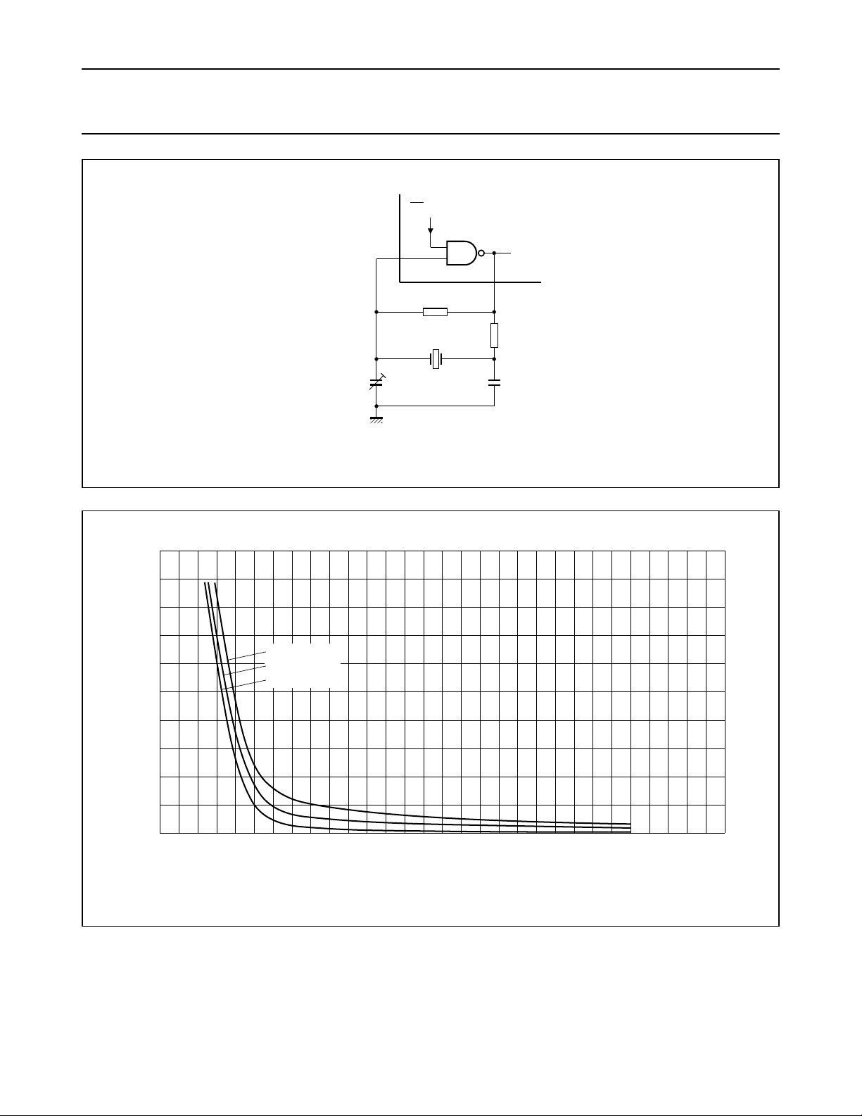
Figure 16 is valid for an external clock
where the trigger is synchronized to
the falling edge of the clock only. The
graph shows that the minimum
programmed pulse width of 100 ns is:
• minimum of 4% too long
• typically 7% too long
• maximum of 10% too long.
September 1993 22
Page 23
Philips Semiconductors Product specification
Programmable delay timer with oscillator 74HC/HCT5555
handbook, full pagewidth
40
36
32
handbook, halfpage
C3
MR (from logic)
RS1
R
bias
100 kΩ to 1 M Ω
22 to
37 pF
R
TC
2
R2
2.2 kΩ
C2 100 pF
MLB336
Fig.15 External components configuration for a crystal oscillator.
MGA648
deviation (%)
28
24
20
16
12
8
4
0
0 200 300
max. expected
typ. expected
min. expected
100 500400
Fig.16 Graphic representation of short time delay accuracy; one stage selected; VCC = 4.5 V.
PACKAGE OUTLINES
See
“74HC/HCT/HCU/HCMOS Logic Package Outlines”
600
programmed time (ns)
.
September 1993 23
 Loading...