

Page 1

INTEGRATED CIRCUITS
DATA SH EET
For a complete data sheet, please also download:
•The IC06 74HC/HCT/HCU/HCMOS Logic Family Specifications
•The IC06 74HC/HCT/HCU/HCMOS Logic Package Information
•The IC06 74HC/HCT/HCU/HCMOS Logic Package Outlines
74HC/HCT4352
Dual 4-channel analog
multiplexer/demultiplexer with latch
Product specification
File under Integrated Circuits, IC06
December 1990
Page 2

Philips Semiconductors Product specification
Dual 4-channel analog
multiplexer/demultiplexer with latch
FEATURES
• Wide analog input voltage range: ± 5V.
• Low “ON” resistance:
80 Ω (typ.) at VCC− VEE= 4.5 V
70 Ω (typ.) at VCC− VEE= 6.0 V
60 Ω (typ.) at VCC− VEE= 9.0 V
• Logic level translation:
to enable 5 V logic to communicate with ± 5 V analog
signals
• Typical “break before make” built in
• Address latches provided
• Output capability: non-standard
• ICC category: MSI
GENERAL DESCRIPTION
The 74HC/HCT4352 are high-speed Si-gate CMOS
devices. They are specified in compliance with JEDEC
standard no. 7A.
The 74HC/HCT4352 are dual 4-channel analog
multiplexers/demultiplexers with common select logic.
74HC/HCT4352
Each multiplexer has four independent inputs/outputs
to nY3) and a common input/output (nZ).
(nY
0
The common channel select logics include two select
inputs (S0 and S1), an active LOW enable input (E1), an
active HIGH enable input (E2) and a latch enable input
(LE).
With E1 LOW and E2 HIGH, one of the four switches is
selected (low impedance ON-state) by S0 and S1. The data
at the select inputs may be latched by using the active
LOW latch enable input (LE). When LE is HIGH, the latch
is transparent. When either of the two enable inputs, E
(active LOW) and E2 (active HIGH), is inactive, all analog
switches are turned off.
VCCand GND are the supply voltage pins for the digital
control inputs (S0, S1, LE, E1 and E2). The VCC to GND
ranges are 2.0 to 10.0 V for HC and 4.5 to 5.5 V for HCT.
The analog inputs/outputs (nY0 to nY3, and nZ) can swing
between VCC as a positive limit and VEE as a negative limit.
VCC− VEE may not exceed 10.0 V.
For operation as a digital multiplexer/demultiplexer, VEE is
connected to GND (typically ground).
1
QUICK REFERENCE DATA
VEE= GND = 0 V; T
=25°C; tr=tf= 6 ns
amb
SYMBOL PARAMETER CONDITIONS
t
PZH
t
PHZ
C
C
C
I
PD
S
/ t
PZL
/ t
PLZ
turn “ON” time E1, E2or Snto V
turn “OFF” time E1, E2or Sn to V
os
os
CL= 15 pF; RL=1kΩ;
VCC=5 V
input capacitance 3.5 3.5 pF
power dissipation capacitance per switch notes 1 and 2 55 55 pF
max. switch capacitance
independent (Y) 5 5 pF
common (Z) 12 12 pF
Notes
1. C
is used to determine the dynamic power dissipation (PD in µW):
PD
PD=CPD× V
2
× fi+∑{ (CL+ CS)×V
CC
2
× fo} where:
CC
fi= input frequency in MHz
fo= output frequency in MHz
∑ {(CL+ CS)×V
2
× fo} = sum of outputs
CC
CL= output load capacitance in pF
CS = max. switch capacitance in pF
VCC= supply voltage in V
2. For HC the condition is VI= GND to V
CC
For HCT the condition is VI= GND to VCC− 1.5 V
TYPICAL
UNIT
HC HCT
31 33 ns
20 20 ns
December 1990 2
Page 3

Philips Semiconductors Product specification
Dual 4-channel analog
multiplexer/demultiplexer with latch
ORDERING INFORMATION
See
“74HC/HCT/HCU/HCMOS Logic Package Information”
PIN DESCRIPTION
PIN NO. SYMBOL NAME AND FUNCTION
1, 6, 2, 5 2Y
to 2Y
0
3
3, 14 n.c. not connected
7
8E
9V
E
1
2
EE
10 GND ground (0 V)
11
13, 12 S
16, 18, 19, 15 1Y
LE latch enable input (active LOW)
, S
0
1
to 1Y
0
3
17, 4 1Z, 2Z common inputs/outputs
20 V
CC
.
independent inputs/outputs
enable input (active LOW)
enable input (active HIGH)
negative supply voltage
select inputs
independent inputs/outputs
positive supply voltage
74HC/HCT4352
Fig.1 Pin configuration. Fig.2 Logic symbol. Fig.3 IEC logic symbol.
December 1990 3
Page 4
Philips Semiconductors Product specification
Dual 4-channel analog
multiplexer/demultiplexer with latch
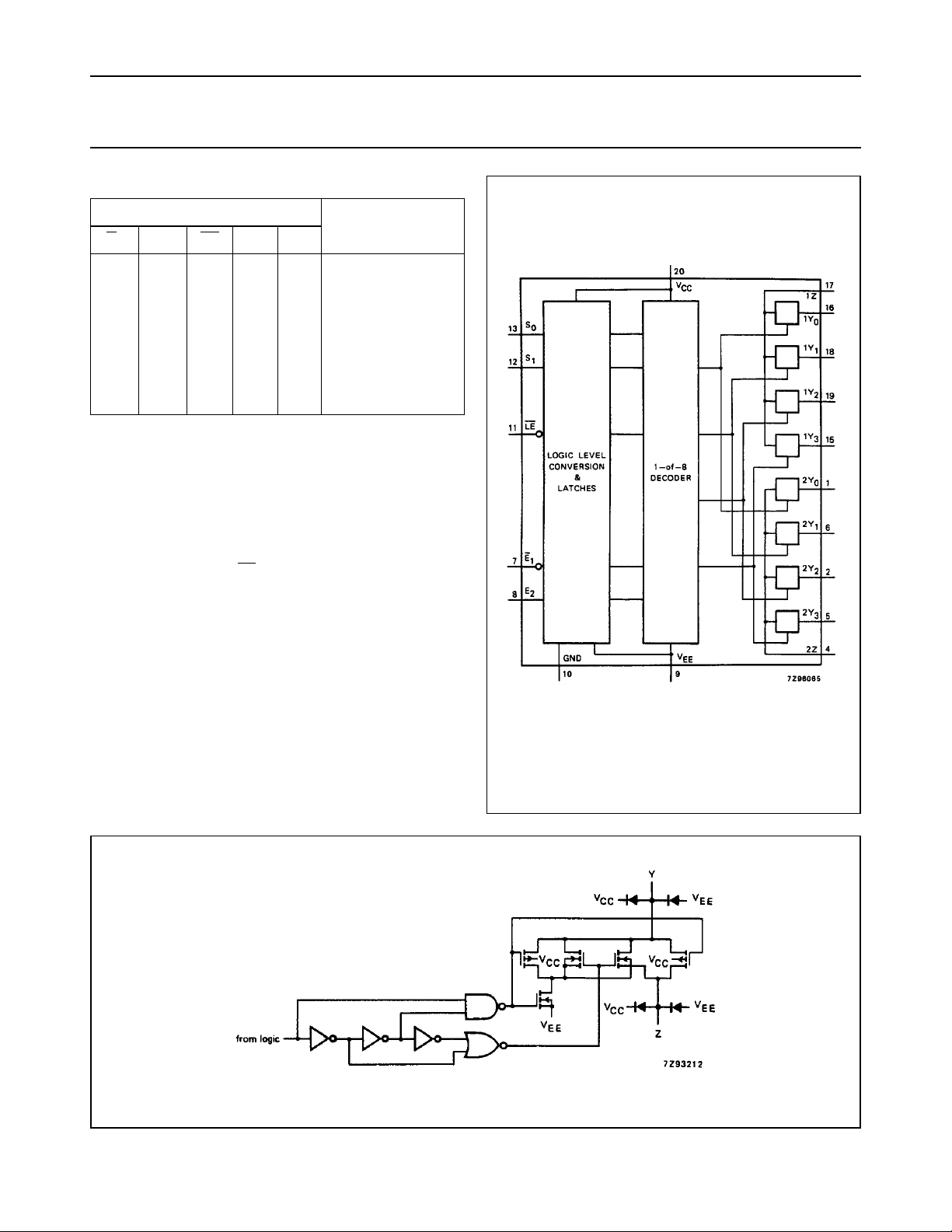
FUNCTION TABLE
INPUTS
E
H
X
L
L
L
L
L
X
E
1
X
L
H
H
H
H
H
X
2
LE S
X
X
H
H
H
H
L
↓
1
X
X
X
X
L
L
L
H
H
L
H
H
X
X
X
X
Notes
1. Last selected channel “ON”.
2. Selected channels latched.
H = HIGH voltage level
L = LOW voltage level
X = don’t care
↓ = HIGH-to-LOW
LE transition
S
CHANNEL ON
0
none
none
nY
0
nY1− nZ
nY2− nZ
nY3− nZ
(1)
(2)
− nZ
74HC/HCT4352
APPLICATIONS
• Analog multiplexing and demultiplexing
• Digital multiplexing and demultiplexing
• Signal gating
Fig.4 Functional diagram.
Fig.5 Schematic diagram (one switch).
December 1990 4
Page 5

Philips Semiconductors Product specification
Dual 4-channel analog
74HC/HCT4352
multiplexer/demultiplexer with latch
RATINGS
Limiting values in accordance with the Absolute Maximum System (IEC 134)
Voltages are referenced to VEE= GND (ground=0V)
SYMBOL PARAMETER MIN. MAX. UNIT CONDITIONS
V
CC
±I
IK
±I
SK
±I
S
±I
EE
±I
;
CC
±I
GND
T
stg
P
tot
P
S
DC supply voltage −0.5 +11.0 V
DC digital input diode current 20 mA for VI< −0.5 V or VI> VCC+ 0.5 V
DC switch diode current 20 mA for VS< −0.5 V or VS> VCC+ 0.5 V
DC switch current 25 mA for −0.5 V < VS<VCC+ 0.5 V
DC VEE current 20 mA
DC VCC or GND current 50 mA
storage temperature range −65 +150 °C
power dissipation per package for temperature range: −40 to +125 °C
74HC/HCT
plastic DIL 750 mW above +70 °C: derate linearly with 12 mW/K
plastic mini-pack (SO) 500 mW above +70 °C: derate linearly with 6 mW/K
power dissipation per switch 100 mW
Note
1. To avoid drawing V
current out of terminals nZ, when switch current flows in terminals nYn, the voltage drop across
CC
the bidirectional switch must not exceed 0.4 V. If the switch current flows into terminals nZ, no VCCcurrent will flow
out of terminals nYn. In this case there is no limit for the voltage drop across the switch, but the voltages at nYn and
nZ may not exceed VCC or VEE.
RECOMMENDED OPERATING CONDITIONS
74HC 74HCT
SYMBOL PARAMETER
UNIT CONDITIONS
min. typ. max. min. typ. max.
V
CC
V
CC
V
I
V
S
T
amb
T
amb
t
, t
r
DC supply voltage VCC−GND 2.0 5.0 10.0 4.5 5.0 5.5 V see Figs 6 and 7
DC supply voltage VCC−V
EE
DC input voltage range GND V
DC switch voltage range V
operating ambient temperature range −40 +85 −40 +85 °C
operating ambient temperature range −40 +125 −40 +125 °C
input rise and fall times
f
2.0 5.0 10.0 2.0 5.0 10.0 V see Figs 6 and 7
EE
GND V
CC
V
CC
V
EE
V
CC
CC
V
V
see DC and AC
CHARACTERISTICS
6.0
1000
500
400
250
6.0 500 ns
VCC= 2.0 V
VCC= 4.5 V
VCC= 6.0 V
VCC= 10.0 V
December 1990 5
Page 6
Philips Semiconductors Product specification
Dual 4-channel analog
multiplexer/demultiplexer with latch
MBA334
VCC- VEE(V)
(V)
10
8
6
4
2
0
0246810
operating area
handbook, halfpage
VCC- GND
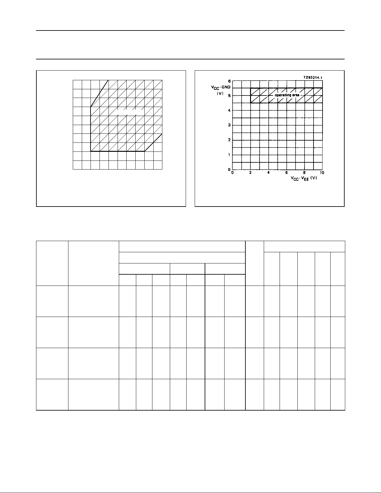
Fig.6 Guaranteed operating area as a function of
the supply voltages for 74HC4352.
DC CHARACTERISTICS FOR 74HC/HCT
For 74HC: V
For 74HCT: V
− GND or VCC− VEE= 2.0, 4.5, 6.0 and 9.0 V
CC
− GND = 4.5 and 5.5 V; VCC− VEE= 2.0, 4.5, 6.0 and 9.0 V
CC
74HC/HCT4352
Fig.7 Guaranteed operating area as a function of
the supply voltages for 74HCT4352.
T
amb
(°C)
TEST CONDITIONS
74HC/HCT
SYMBOL PARAMETER
+25 −40 to +85 −40 to +125
UNIT
V
(V)
CC
V
(V)
EE
(µA)
min. typ. max. min. max. min. max.
R
R
R
∆R
ON
ON
ON
ON
ON resistance
(peak)
ON resistance
(rail)
ON resistance
(rail)
maximum ∆ON
resistance
between any two
channels
−
100
90
70
150
80
70
60
150
90
80
65
−
9
8
6
−
180
160
130
−
140
120
105
−
160
140
120
−
225
200
165
−
175
150
130
−
200
175
150
−
270
240
195
−
210
180
160
−
240
210
180
Ω
2.0
0
100
Ω
4.5
Ω
6.0
Ω
4.5
Ω
2.0
Ω
4.5
Ω
6.0
Ω
4.5
Ω
2.0
Ω
4.5
Ω
6.0
Ω
4.5
Ω
2.0
Ω
4.5
Ω
6.0
Ω
4.5
0
0
−4.5
0
0
0
−4.5
0
0
0
−4.5
0
0
0
−4.5
1000
1000
1000
100
1000
1000
1000
100
1000
1000
1000
Notes
1. At supply voltages (V
− VEE) approaching 2.0 V the analog switch ON-resistance becomes extremely non-linear.
CC
There it is recommended that these devices be used to transmit digital signals only, when using these supply
voltages.
2. For test circuit measuring RON see Fig.8.
I
S
VisV
V
CC
to
V
EE
VEEV
VCCV
V
CC
to
V
EE
V
or
V
or
V
or
V
V
or
V
I
IN
IL
IH
IL
IH
IL
IH
IL
December 1990 6
Page 7
Philips Semiconductors Product specification
Dual 4-channel analog
multiplexer/demultiplexer with latch
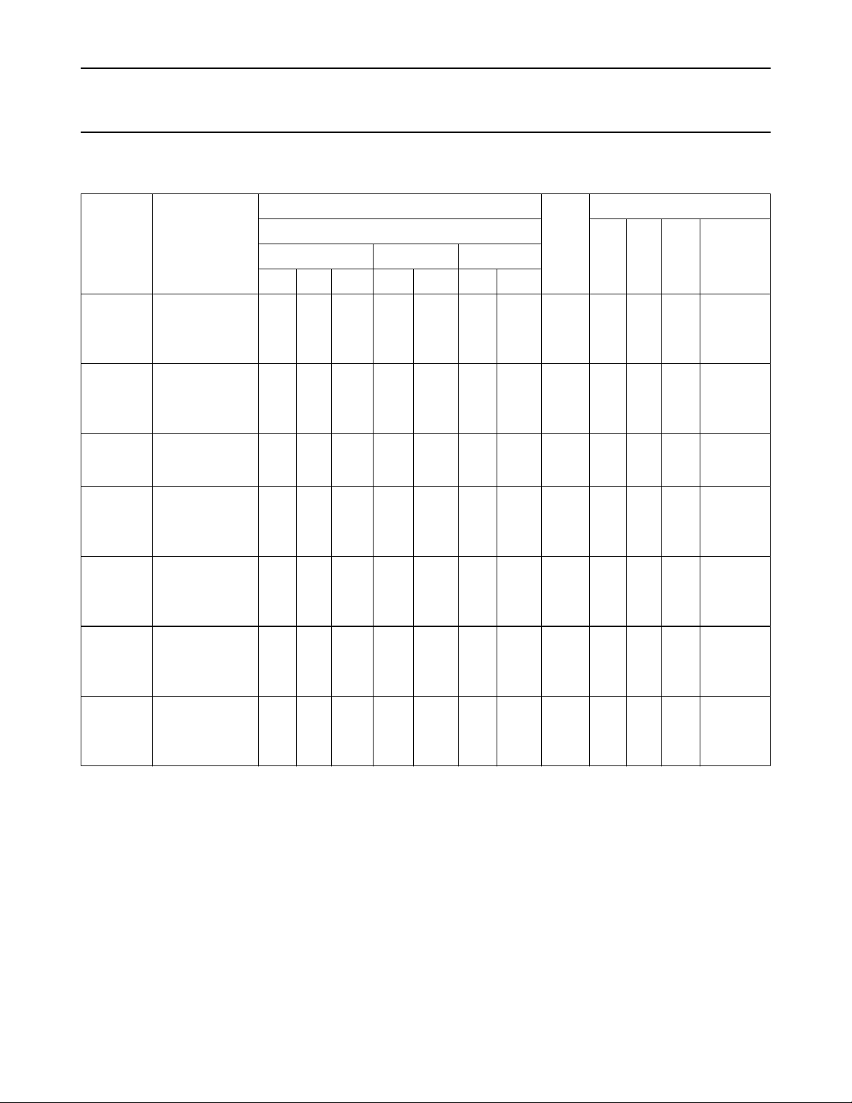
DC CHARACTERISTICS FOR 74HC
Voltages are referenced to GND (ground = 0 V)
SYMBOL PARAMETER
min. typ. max. min. max. min. max.
V
V
±I
±I
±I
±I
I
CC
IH
HIGH level input
voltage
IL
LOW level input
voltage
I
input leakage
current
S
analog switch
OFF-state
current per
channel
S
analog switch
OFF-state
current all
channels
S
analog switch
ON-state
current
quiescent
supply current
1.5
3.15
4.2
6.3
1.2
2.4
3.2
4.7
0.8
0.5
2.1
1.35
2.8
1.8
4.3
2.7
0.1
0.2
0.1 1.0 1.0 µA 10.0 0V
0.2 2.0 2.0 µA 10.0 0V
0.2 2.0 2.0 µA 10.0 0V
8.0
16.0
T
amb
74HC
1.5
3.15
4.2
6.3
(°C)
0.5
1.35
1.8
2.7
1.0
2.0
80.0
160.0
1.5
3.15
4.2
6.3
0.5
1.35
1.8
2.7
1.0
2.0
160.0
320.0
UNIT
V
(V)
V 2.0
4.5
6.0
9.0
V 2.0
4.5
6.0
9.0
µA 6.0
10.0
µA 6.0
10.0
74HC/HCT4352
TEST CONDITIONS
V
CC
EE
V
OTHER+25 −40 to +85 −40 to +125
V
CC
or
GND
IH
or
V
IL
IH
or
V
IL
IH
or
V
IL
V
CC
or
GND
I
|VS|=V
− V
EE
(see
Fig.10)
|VS|=V
− V
EE
(see
Fig.10)
|VS|= V
− V
EE
(see
Fig.11)
V
iS=VEE
or VCC; V
= VCC or
V
EE
(V)
0
0
0
0
CC
CC
CC
os
December 1990 7
Page 8
Philips Semiconductors Product specification
Dual 4-channel analog
multiplexer/demultiplexer with latch
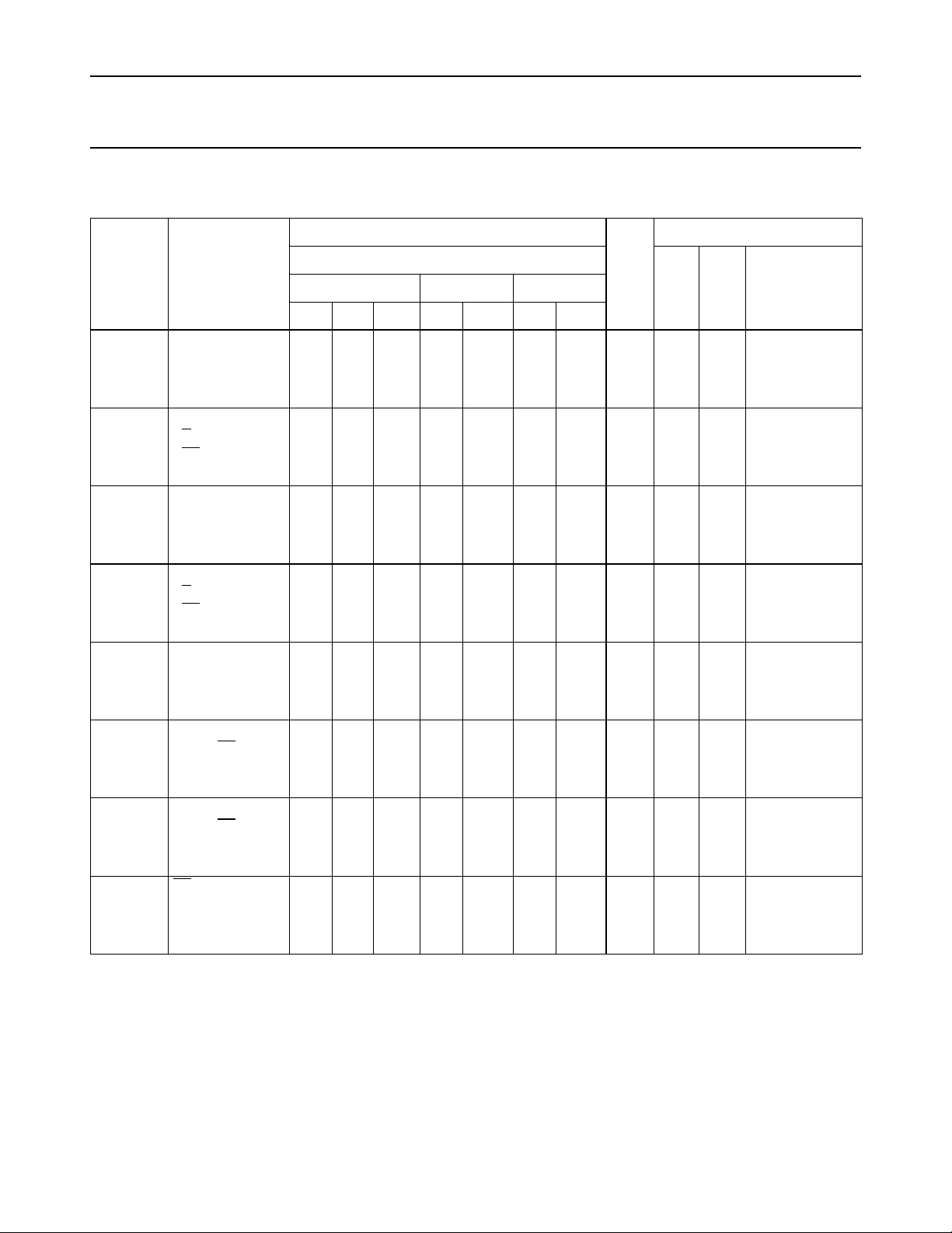
AC CHARACTERISTICS FOR 74HC
GND = 0 V; t
SYMBOL PARAMETER
/ t
t
PHL
PLH
t
/ t
PZH
PZL
t
/ t
PZH
PZL
t
/ t
PHZ
PLZ
/ t
t
PHZ
PLZ
t
su
t
h
t
W
= 6 ns; CL=50pF
r=tf
propagation
delay
Vis to V
os
turn “ON” time
E1; E2to V
LE to V
os
os
turn “ON” time
Sn to V
os
turn “OFF” time
E1; E2 to V
LE to V
os
os
turn “OFF” time
Sn to V
os
set-up time
Sn to LE
hold time
Sn to LE
LE minimum
pulse width
HIGH
min. typ. max. min. max. min. max.
17
60
6
12
5
10
5
8
99
325
36
65
29
55
25
46
99
325
36
65
29
55
25
46
58
200
21
40
17
34
21
40
63
200
23
40
18
34
24
40
90
17
18
6
15
5
18
9
5
−6
5
−2
5
−2
5
−3
80
11
16
4
14
3
16
4
T
amb
115
23
20
23
5
5
5
5
100
20
17
20
(°C)
74HC
75
15
13
10
405
81
69
58
405
81
69
58
250
50
43
50
250
50
43
50
135
27
23
27
5
5
5
5
120
24
20
24
90
18
15
12
490
98
83
69
490
98
80
69
300
60
51
60
300
60
51
60
UNIT
V
(V)
ns 2.0
4.5
6.0
4.5
ns 2.0
4.5
6.0
4.5
ns 2.0
4.5
6.0
4.5
ns 2.0
4.5
6.0
4.5
ns 2.0
4.5
6.0
4.5
ns 2.0
4.5
6.0
4.5
ns 2.0
4.5
6.0
4.5
ns 2.0
4.5
6.0
4.5
74HC/HCT4352
TEST CONDITIONS
V
CC
EE
(V)
0
0
0
−4.5
0
0
0
−4.5
0
0
0
−4.5
0
0
0
−4.5
0
0
0
−4.5
0
0
0
−4.5
0
0
0
−4.5
0
0
0
−4.5
OTHER+25 −40 to +85 −40 to +125
RL= ∞;
CL=50pF
(see Fig.18)
RL=1kΩ;
CL=50pF
(see Fig.19)
RL=1kΩ;
CL=50pF
(see Fig.19)
RL=1kΩ;
CL=50pF
(see Fig.19)
RL=1kΩ;
CL=50pF
(see Fig.19)
RL=1kΩ;
CL=50pF
(see Fig.20)
RL=1kΩ;
CL=50pF
(see Fig.20)
RL=1kΩ;
CL=50pF
(see Fig.20)
December 1990 8
Page 9
Philips Semiconductors Product specification
Dual 4-channel analog
multiplexer/demultiplexer with latch
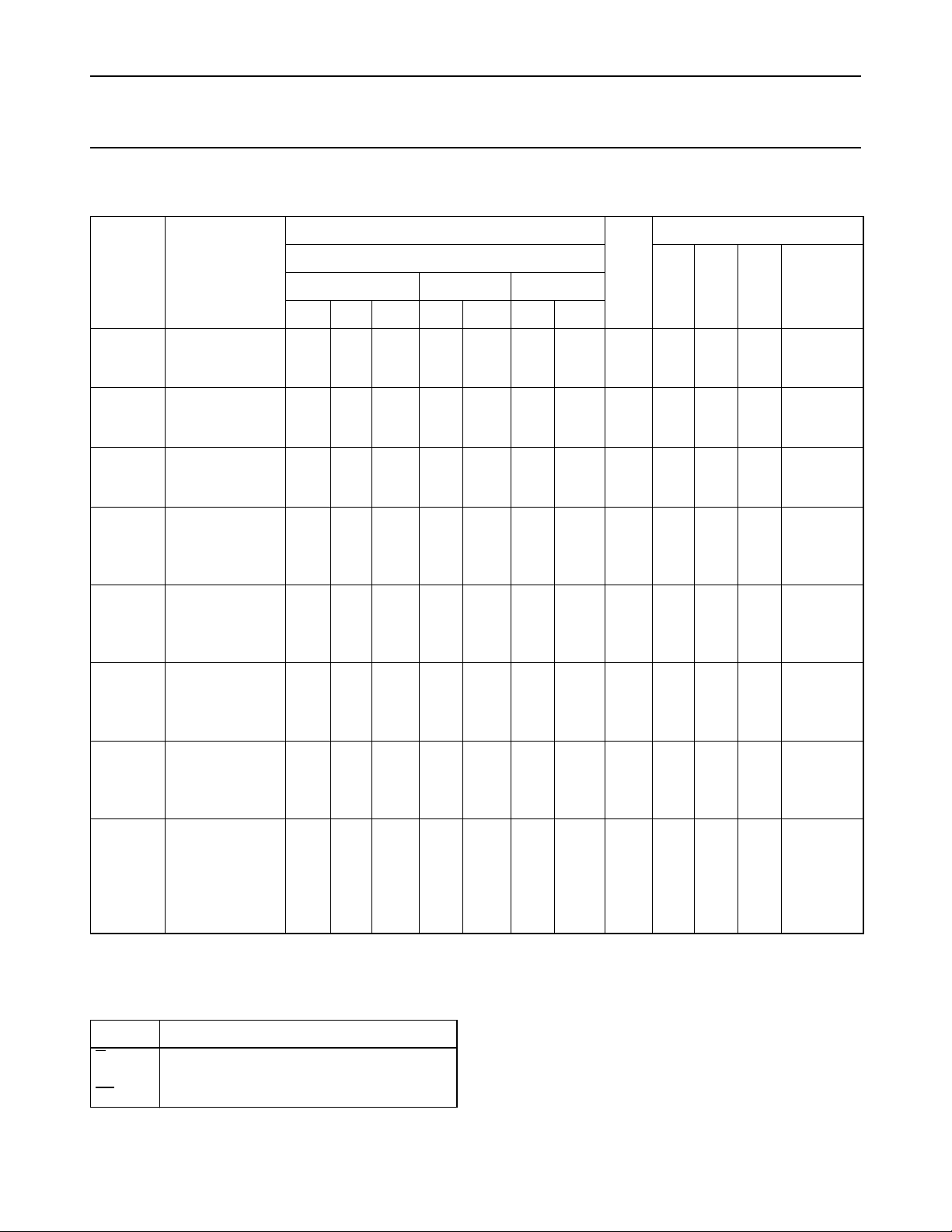
DC CHARACTERISTICS FOR 74HCT
Voltages are referenced to GND (ground = 0)
SYMBOL PARAMETER
min. typ. max. min. max. min. max.
V
V
±I
±I
±I
±I
I
∆I
CC
IH
IL
I
S
S
S
CC
HIGH level
input voltage
LOW level input
voltage
input leakage
current
analog switch
OFF-state
current per
channel
analog switch
OFF-state
current all
channels
analog switch
ON-state current
quiescent supply
current
additional
quiescent supply
current per
input pin for unit
load coefficient
is 1 (note 1)
2.0 1.6 2.0 2.0 V 4.5
1.2 0.8 0.8 0.8 V 4.5
0.1 1.0 1.0 µA 5.5 0 V
0.1 1.0 1.0 µA 10.0 0 V
0.2 2.0 2.0 µA 10.0 0 V
0.2 2.0 2.0 µA 10.0 0 V
8.0
16.0
100 360 450 490 µA 4.5
T
amb
74HCT
(°C)
80.0
160.0
160.0
320.0
UNIT
V
(V)
to
5.5
to
5.5
µA 5.5
5.00−5.0
to
5.5
74HC/HCT4352
TEST CONDITIONS
V
CC
EE
V
OTHER+25 −40 to +85 −40 to +125
CC
or
GND
IH
or
V
IL
IH
or
V
IL
IH
or
V
IL
V
CC
or
GND
CC
− 2.1
V
I
|VS|=V
− V
(see
Fig.10)
|VS|=V
− V
(see
Fig.10)
|VS|=V
− V
(see
Fig.11)
ViS=V
or VCC;
Vos= V
or V
other
inputs at
VCC or
GND
(V)
0V
CC
EE
CC
EE
CC
EE
EE
CC
EE
Note to HCT types
1. The value of additional quiescent supply current (∆I
) for a unit load of 1 is given here. To determine ∆ICC per input,
CC
multiply this value by the unit load coefficient shown in the table below.
INPUT UNIT LOAD COEFFICIENT
E1, E
S
n
LE
0.50
2
0.50
1.5
December 1990 9
Page 10
Philips Semiconductors Product specification
Dual 4-channel analog
multiplexer/demultiplexer with latch
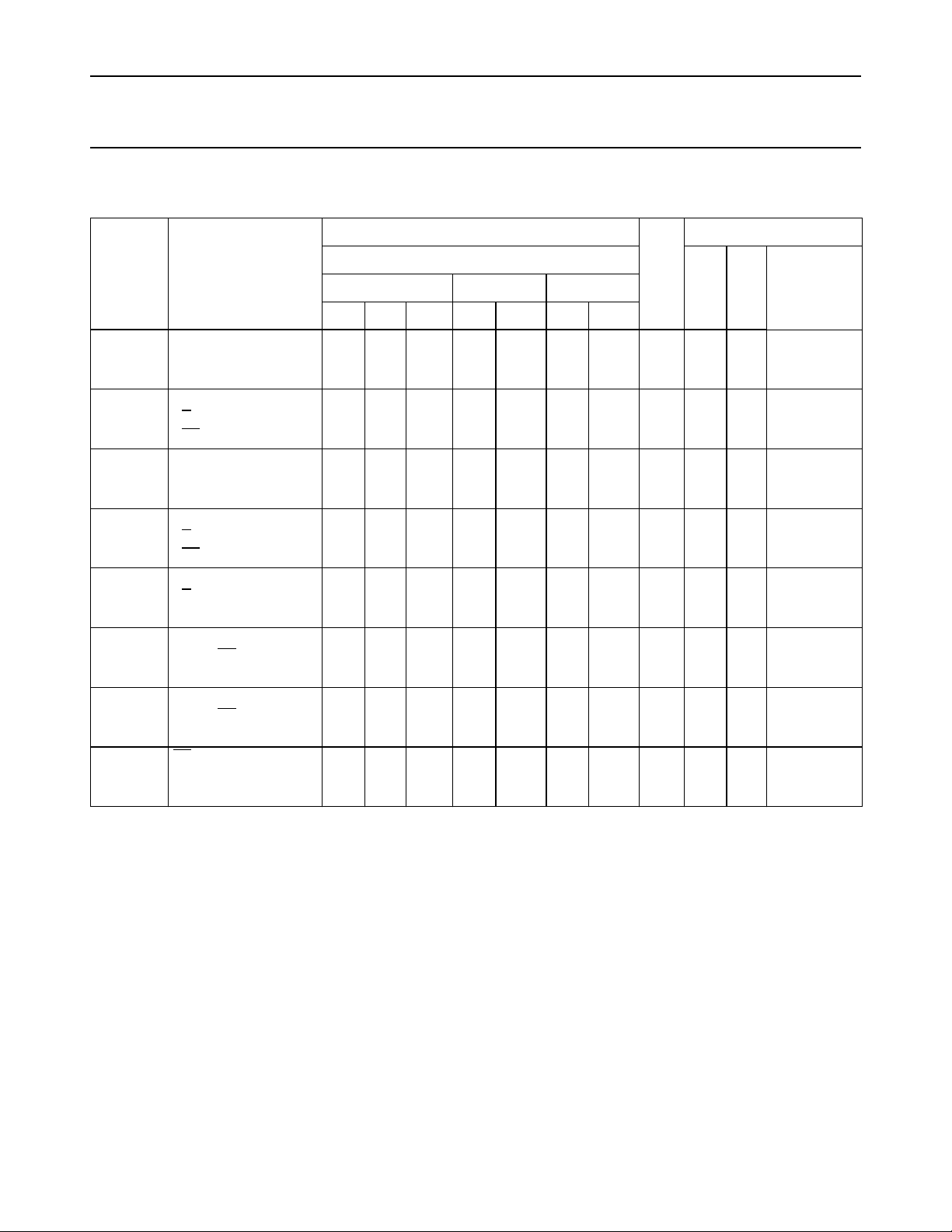
AC CHARACTERISTICS FOR 74HCT
GND = 0 V; t
SYMBOL PARAMETER
/ t
t
PHL
PLH
/ t
t
PZH
PZL
t
/ t
PZH
PZL
t
/ t
PHZ
PLZ
t
/ t
PHZ
PLZ
t
su
t
h
t
W
= 6 ns; CL=50pF
r=tf
propagation delay
Vis to V
os
turn “ON” time
E1; E2 to V
LE to V
os
os
turn “ON” time
Sn to V
os
turn “OFF” time
E1 to V
os
LE to V
os
turn “OFF” time
E2, Sn to V
os
set-up time
Sn to LE
hold time
Sn to LE
LE minimum pulse
width HIGH
min. typ. max. min. max. min. max.
6
5
382865
382765
202040
252543
16187
9
5
−1
5
−1
16163
4
12
8
46
46
40
43
T
amb
74HCT
20
23
5
5
20
20
(°C)
15
10
81
58
81
58
50
50
54
54
24
27
5
5
24
24
18
12
98
69
98
69
60
60
65
65
74HC/HCT4352
TEST CONDITIONS
UNIT
ns 4.5
ns 4.5
ns 4.5
ns 4.5
ns 4.5
ns 4.5
ns 4.5
ns 4.5
V
V
CC
EE
(V)
(V)
4.50−4.5
4.50−4.5
4.50−4.5
4.50−4.5
4.50−4.5
4.50−4.5
4.50−4.5
4.50−4.5
OTHER+25 −40 to +85 −40 to +125
RL= ∞;
CL=50pF
(see Fig.18)
RL=1kΩ;
CL=50pF
(see Fig.19)
RL=1kΩ;
CL=50pF
(see Fig.19)
RL=1kΩ;
CL=50pF
(see Fig.19)
RL=1kΩ;
CL=50pF
(see Fig.19)
RL=1kΩ;
CL=50pF
(see Fig.20)
RL=1kΩ;
CL=50pF
(see Fig.20)
RL=1kΩ;
CL=50pF
(see Fig.20)
December 1990 10
Page 11
Philips Semiconductors Product specification
Dual 4-channel analog
multiplexer/demultiplexer with latch
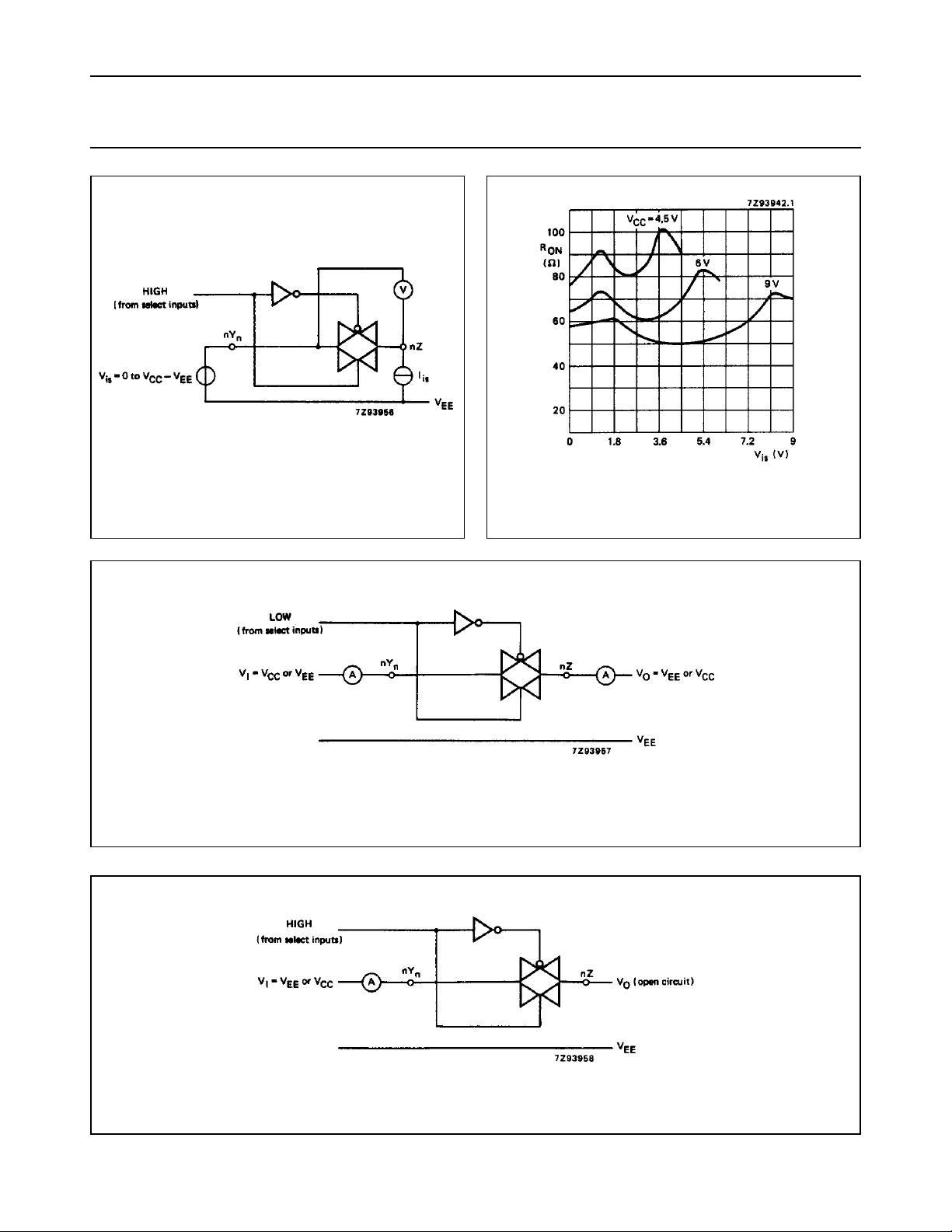
Fig.8 Test circuit for measuring RON.
74HC/HCT4352
Fig.9 Typical RON as a function of input voltage V
for Vis= 0 to VCC− VEE.
is
Fig.10 Test circuit for measuring OFF-state current.
Fig.11 Test circuit for measuring ON-state current.
December 1990 11
Page 12
Philips Semiconductors Product specification
Dual 4-channel analog
multiplexer/demultiplexer with latch
ADDITIONAL AC CHARACTERISTICS FOR 74HC/HCT
Recommended conditions and typical values
GND = 0 V; T
SYMBOL PARAMETER typ. UNIT
V
(p-p)
f
max
C
S
=25°C
amb
sine-wave distortion
f = 1 kHz
sine-wave distortion
f = 10 kHz
switch “OFF” signal
feed-through
crosstalk between
any two switches/
multiplexers
crosstalk voltage between
control and any switch
(peak-to-peak value)
minimum frequency response
(−3dB)
maximum switch capacitance
independent (Y)
common (Z)
0.04
0.02%%
0.12
0.06%%
−50
−50
−60
−60
110
dB
dB
dB
dB
mVmV4.5
220
160
170
5
12
MHz
MHz
pF
pF
V
(V)
2.25
4.5
2.25
4.5
2.25
4.5
2.25
4.5
CC
V
(V)
−2.25
−4.5
−2.25
−4.5
−2.25
−4.5
−2.25
−4.5
4.50−4.5
2.25
4.5
−2.25
−4.5
74HC/HCT4352
V
EE
is(p-p)
(V)
4.0
8.0
4.0
8.0
R
(see Fig.14)
R
(see Fig.14)
note 1 R
f =1 MHz (see Figs 12 and 15)
note 1 R
f = 1 MHz (see Fig.16)
RL= 600 Ω;CL=50pF;
f = 1 MHz (E1, E2 or Sn,
square-wave between VCC and
GND, tr=tf= 6 ns)
(see Fig.17)
note 2 RL=50Ω; CL=10pF
(see Figs 13 and 14)
CONDITIONS
=10kΩ; CL=50pF
L
=10kΩ; CL=50pF
L
= 600 Ω; CL=50pF
L
= 600 Ω; CL=50pF;
L
Notes
1. Adjust input voltage V
to 0 dBm level (0 dBm = 1 mW into 600 Ω).
is
2. Adjust input voltage Visto 0 dBm level at Vos for 1 MHz (0 dBm = 1 mW into 50 Ω).
Vis is the input voltage at an nYn or nZ terminal, whichever is assigned as an input.
Vos is the output voltage at an nYn or nZ terminal, whichever is assigned as an output.
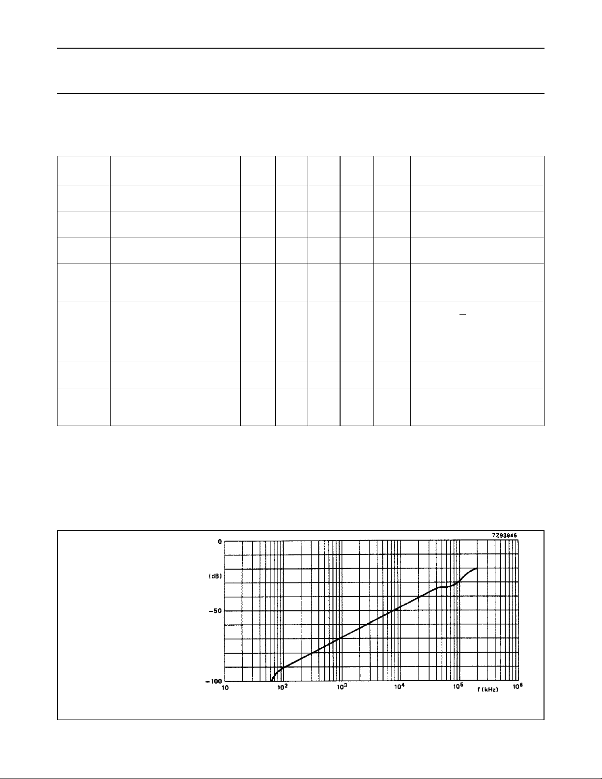
Test conditions:
= 4.5 V; GND = 0 V; VEE= −4.5 V;
V
CC
=50Ω; R
R
L
source
=1kΩ.
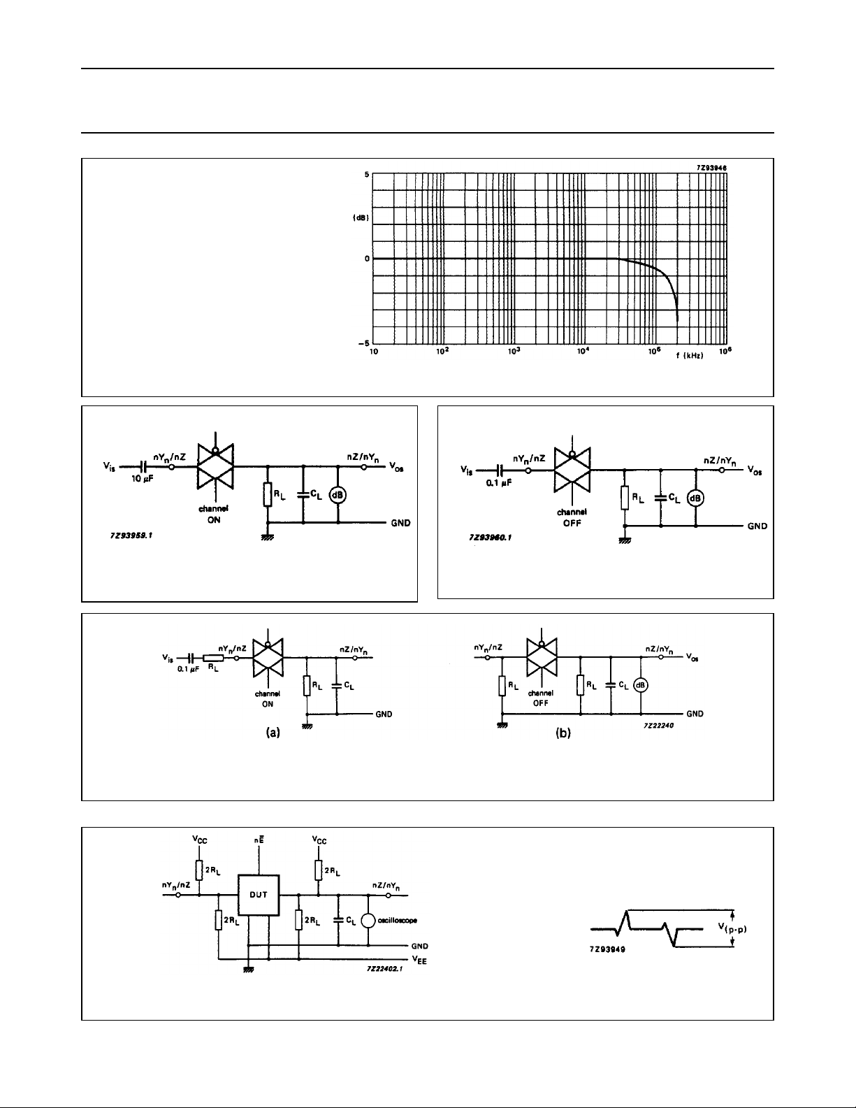
Fig.12 Typical switch “OFF” signal feed-through as a function of frequency.
December 1990 12
Page 13
Philips Semiconductors Product specification
Dual 4-channel analog
multiplexer/demultiplexer with latch
Test conditions:
= 4.5 V; GND = 0 V; VEE= −4.5 V;
V
CC
=50Ω; R
R
L
source
=1kΩ.
Fig.13 Typical frequency response.
74HC/HCT4352
Fig.14 Test circuit for measuring sine-wave
distortion and minimum frequency response.
Fig.16 Test circuits for measuring crosstalk between any two switches/multiplexers.
(a) channel ON condition; (b) channel OFF condition.
Fig.15 Test circuit for measuring switch “OFF” signal
feed-through.
The crosstalk is defined as
follows (oscilloscope output):
Fig.17 Test circuit for measuring crosstalk between control and any switch.
December 1990 13
Page 14
Philips Semiconductors Product specification
Dual 4-channel analog
multiplexer/demultiplexer with latch
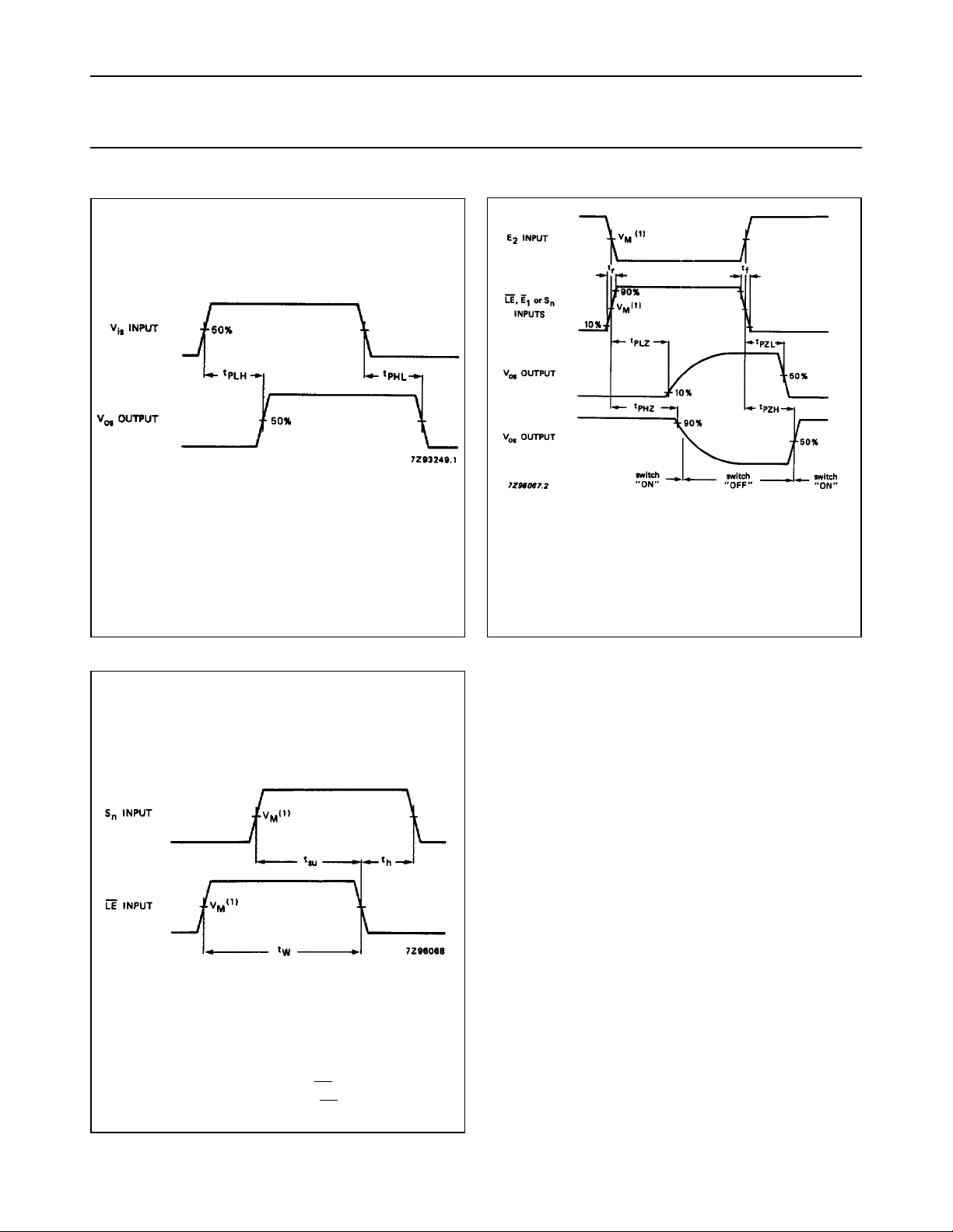
AC WAVEFORMS
74HC/HCT4352
(1) HC : VM= 50%; VI= GND to VCC.
HCT: V
= 1.3 V; VI= GND to 3 V.
M
Fig.18 Waveforms showing the input (Vis) to output
(Vos) propagation delays.
(1) HC : VM= 50%; VI= GND to VCC.
= 1.3 V; VI= GND to 3 V.
HCT: V
M
Fig.19 Waveforms showing the turn-ON and
turn-OFF times.
Fig.20 Waveforms showing the set-up and hold
times from Sn inputs to LE input, and
minimum pulse width of LE.
December 1990 14
Page 15
Philips Semiconductors Product specification
Dual 4-channel analog
74HC/HCT4352
multiplexer/demultiplexer with latch
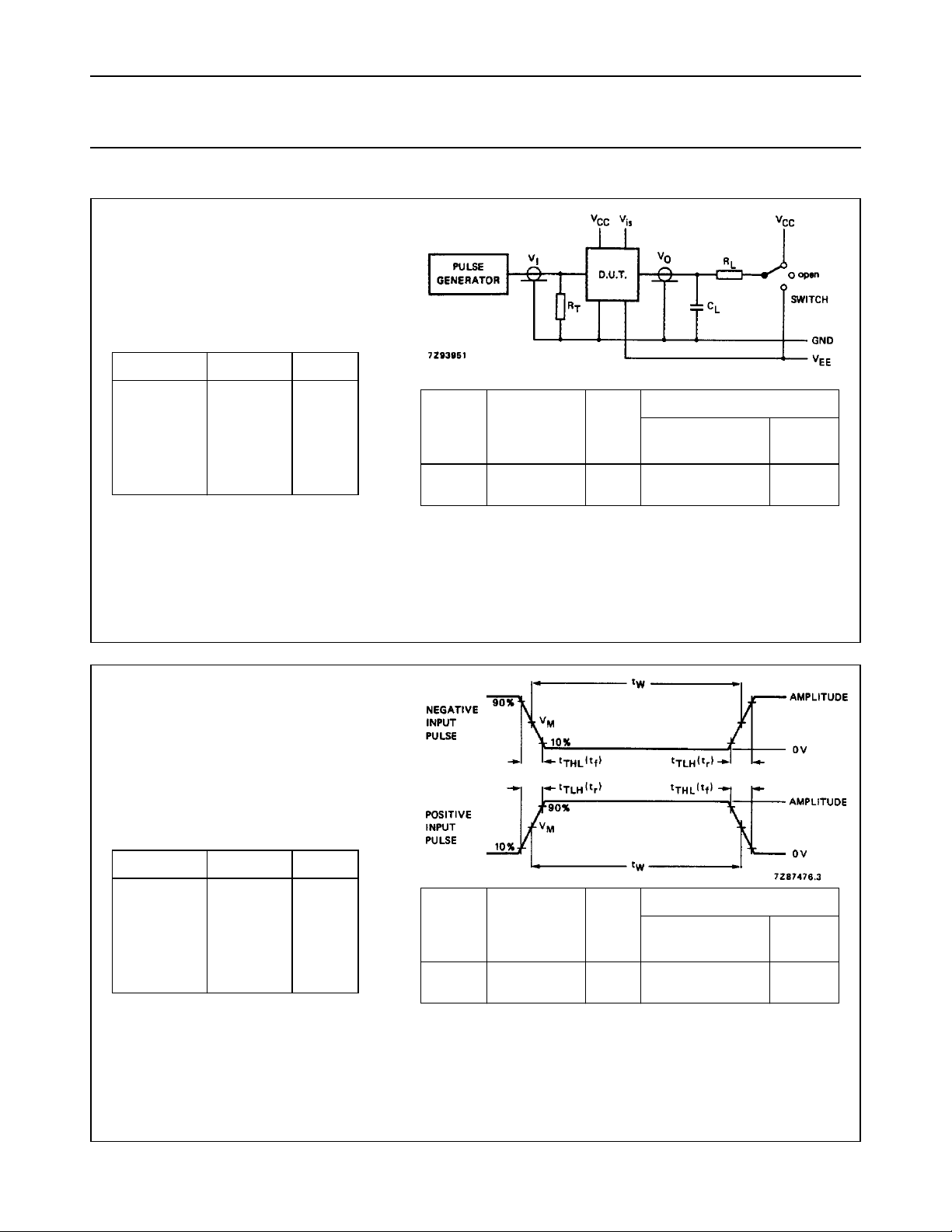
TEST CIRCUIT AND WAVEFORMS
Conditions
TEST SWITCH V
t
PZH
t
PZL
t
PHZ
t
PLZ
V
EE
V
CC
V
EE
V
CC
others open pulse
CL= load capacitance including jig and probe capacitance (see AC CHARACTERISTICS for values).
R
= termination resistance should be equal to the output impedance ZO of the pulse generator.
T
t
=tf= 6 ns; when measuring f
r
is
V
CC
V
EE
V
CC
V
EE
, there is no constraint on tr, tf with 50% duty factor.
max
FAMILY AMPLITUDE V
74HC
74HCT
V
CC
3.0 V
50%
1.3 V
M
PULSE WIDTH
< 2ns
<2ns
f
max
;
tr; t
f
OTHER
6ns
6ns
Fig.21 Test circuit for measuring AC performance.
Conditions
TEST SWITCH V
t
PZH
t
PZL
t
PHZ
t
PLZ
V
EE
V
CC
V
EE
V
CC
others open pulse
is
V
CC
V
EE
V
CC
V
EE
FAMILY AMPLITUDE V
74HC
74HCT
V
CC
3.0 V
50%
1.3 V
M
PULSE WIDTH
< 2ns
<2ns
f
max
;
tr; t
f
CL= load capacitance including jig and probe capacitance (see AC CHARACTERISTICS for values).
= termination resistance should be equal to the output impedance ZO of the pulse generator.
R
T
t
=tf= 6 ns; when measuring f
r
, there is no constraint on tr, tf with 50% duty factor.
max
OTHER
6ns
6ns
Fig.22 Input pulse definitions.
December 1990 15
Page 16

Philips Semiconductors Product specification
Dual 4-channel analog
multiplexer/demultiplexer with latch
PACKAGE OUTLINES
See
“74HC/HCT/HCU/HCMOS Logic Package Outlines”
74HC/HCT4352
.
December 1990 16
 Loading...