

Page 1
INTEGRATED CIRCUITS
DATA SH EET
For a complete data sheet, please also download:
•The IC06 74HC/HCT/HCU/HCMOS Logic Family Specifications
•The IC06 74HC/HCT/HCU/HCMOS Logic Package Information
•The IC06 74HC/HCT/HCU/HCMOS Logic Package Outlines
74HC/HCT373
Octal D-type transparent latch;
3-state
Product specification
File under Integrated Circuits, IC06
September 1993
Page 2
Philips Semiconductors Product specification
Octal D-type transparent latch; 3-state 74HC/HCT373
FEATURES
• 3-state non-inverting outputs for bus oriented
applications
• Common 3-state output enable input
• Functionally identical to the “563”, “573” and “533”
• Output capability: bus driver
• ICC category: MSI
input and an output enable (
latches.
The “373” consists of eight D-type transparent latches with
3-state true outputs. When LE is HIGH, data at the D
inputs enters the latches. In this condition the latches are
transparent, i.e. a latch output will change state each time
its corresponding D-input changes.
When LE is LOW the latches store the information that was
present at the D-inputs a set-up time preceding the
GENERAL DESCRIPTION
HIGH-to-LOW transition of LE. When OE is LOW, the
contents of the 8 latches are available at the outputs.
The 74HC/HCT373 are high-speed Si-gate CMOS devices
and are pin compatible with low power Schottky TTL
(LSTTL). They are specified in compliance with JEDEC
When OE is HIGH, the outputs go to the high impedance
OFF-state. Operation of the OE input does not affect the
state of the latches.
standard no. 7A.
The “373” is functionally identical to the “533”, “563” and
The 74HC/HCT373 are octal D-type transparent latches
featuring separate D-type inputs for each latch and 3-state
“573”, but the “563” and “533” have inverted outputs and
the “563” and “573” have a different pin arrangement.
outputs for bus oriented applications. A latch enable (LE)
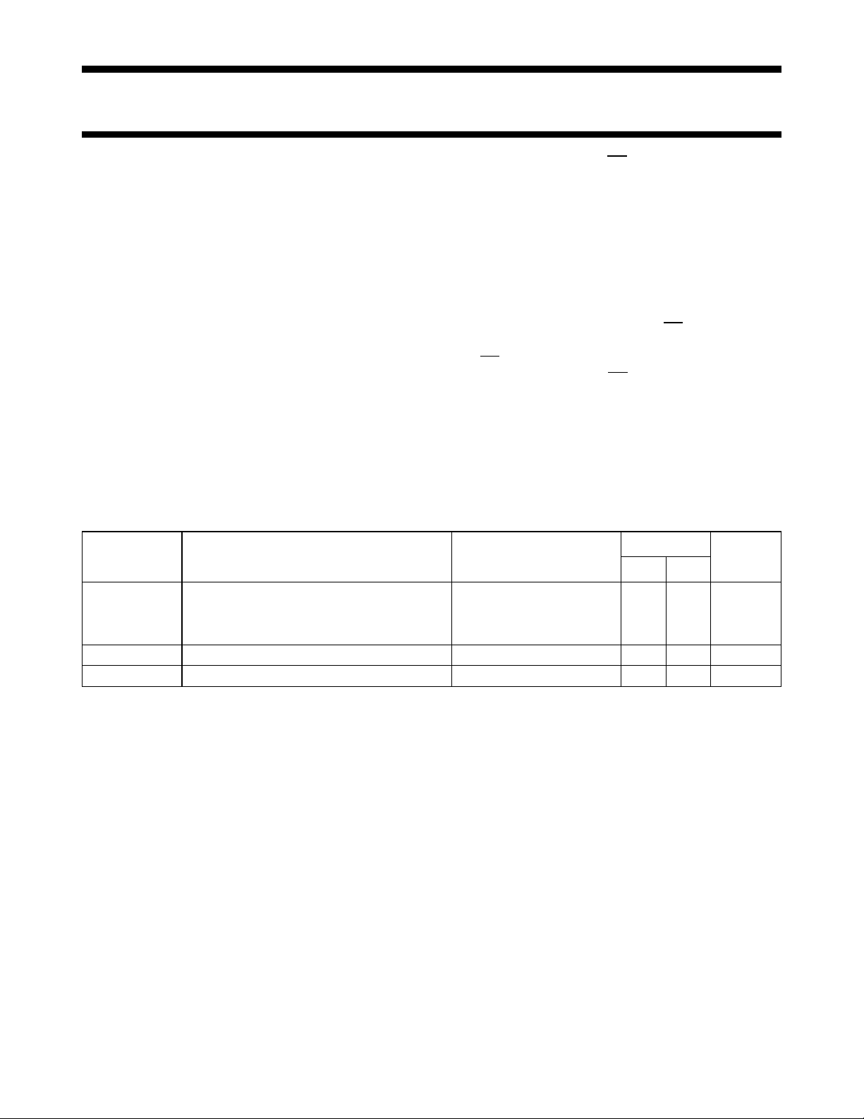
QUICK REFERENCE DATA
GND = 0 V; T
=25°C; tr=tf= 6 ns
amb
SYMBOL PARAMETER CONDITIONS
t
PHL
C
C
I
PD
/ t
PLH
propagation delay CL= 15 pF; VCC=5V
D
to Q
n
n
LE to Q
n
input capacitance 3.5 3.5 pF
power dissipation capacitance per latch notes 1 and 2 45 41 pF
OE) input are common to all
n
TYPICAL
UNIT
HC HCT
12 14 ns
15 13 ns
Notes
1. C
is used to determine the dynamic power dissipation (PD in µW):
PD
PD=CPD× V
2
× fi+∑ (CL× V
CC
2
× fo) where:
CC
fi= input frequency in MHz
fo= output frequency in MHz
∑ (CL× V
2
× fo) = sum of outputs
CC
CL= output load capacitance in pF
VCC= supply voltage in V
2. For HC the condition is VI= GND to VCC. For HCT the condition is VI= GND to VCC− 1.5 V
ORDERING INFORMATION
“74HC/HCT/HCU/HCMOS Logic Package Information”
See
.
September 1993 2
Page 3
Philips Semiconductors Product specification
Octal D-type transparent latch; 3-state 74HC/HCT373
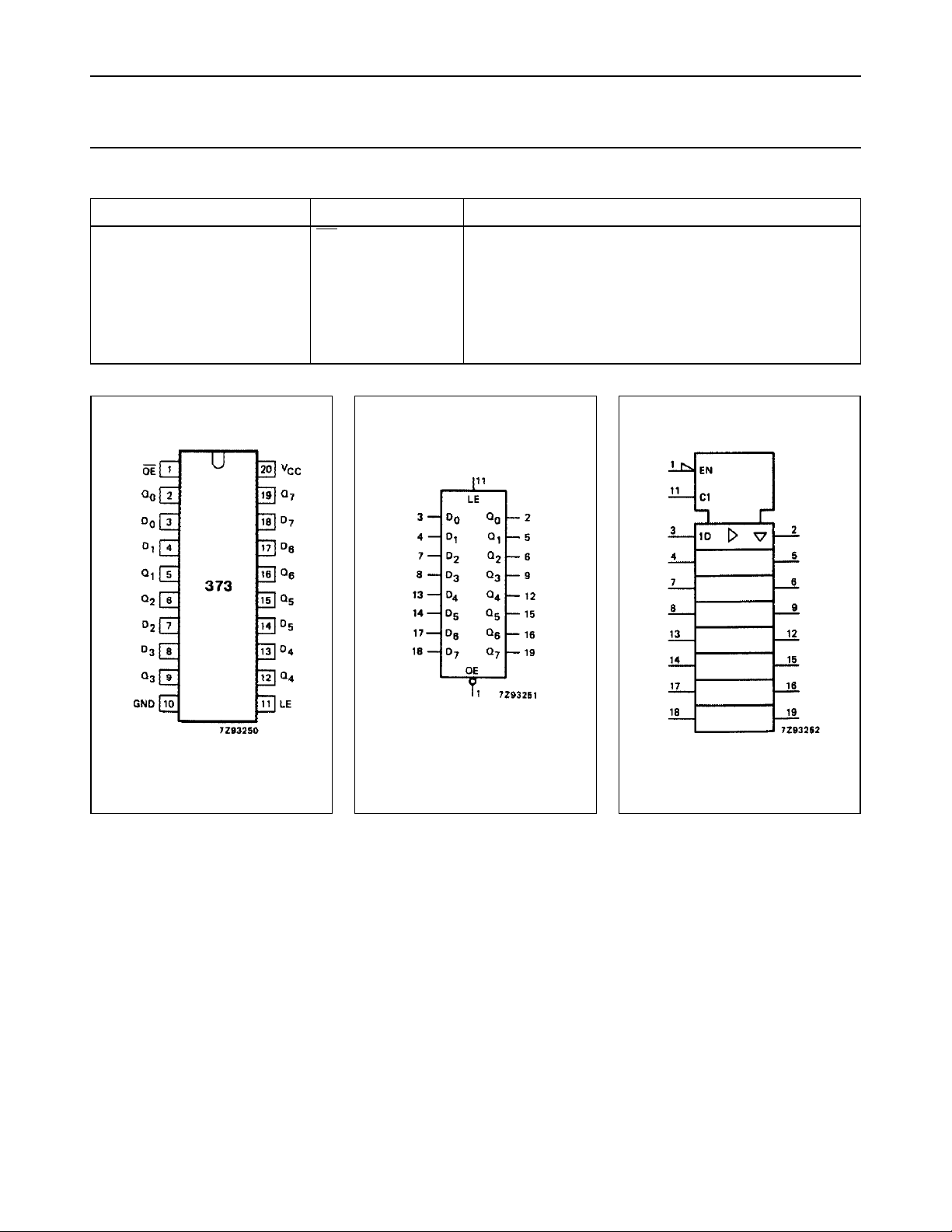
PIN DESCRIPTION
PIN NO. SYMBOL NAME AND FUNCTION
1
2, 5, 6, 9, 12, 15, 16, 19 Q
3, 4, 7, 8, 13, 14, 17, 18 D
10 GND ground (0 V)
11 LE latch enable input (active HIGH)
20 V
OE 3-state output enable input (active LOW)
to Q
0
to D
0
CC
7
7
3-state latch outputs
data inputs
positive supply voltage
Fig.1 Pin configuration. Fig.2 Logic symbol. Fig.3 IEC logic symbol.
September 1993 3
Page 4
Philips Semiconductors Product specification
Octal D-type transparent latch; 3-state 74HC/HCT373
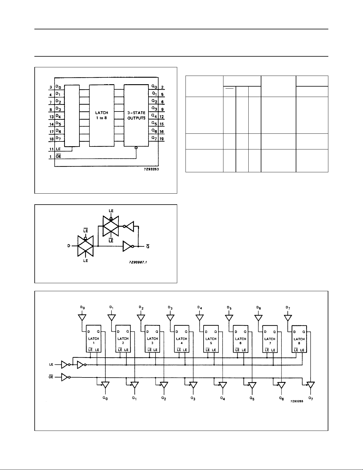
FUNCTION TABLE
Fig.4 Functional diagram.
OPERATING
MODES
enable and
INPUTS
OE LE D
LLHHL
INTERNAL
LATCHES
n
L
read
register
H
H
(transparent
mode)
latch and
read registerLLLLlh
latch register
HHXXX
and disable
X
L
H
X
X
outputs
Notes
1. H = HIGH voltage level
h = HIGH voltage level one set-up time prior to the
HIGH-to-LOW LE transition
L = LOW voltage level
I = LOW voltage level one set-up time prior to the
HIGH-to-LOW LE transition
X = don’t care
Z = high impedance OFF-state
OUTPUTS
Q0to Q
7
L
H
L
H
Z
Z
Fig.5 Logic diagram (one latch).
Fig.6 Logic diagram.
September 1993 4
Page 5
Philips Semiconductors Product specification
Octal D-type transparent latch; 3-state 74HC/HCT373
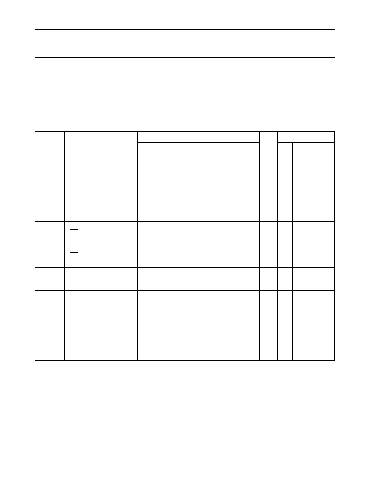
DC CHARACTERISTICS FOR 74HC
For the DC characteristics see
“74HC/HCT/HCU/HCMOS Logic Family Specifications”
Output capability: bus driver
ICC category: MSI
AC CHARACTERISTICS FOR 74HC
GND = 0 V; t
= 6 ns; CL=50pF
r=tf
SYMBOL PARAMETER
t
PHL
t
PHL
t
PZH
t
PHZ
t
THL
t
W
/ t
/ t
/ t
/ t
/ t
propagation delay
PLH
Dn to Q
propagation delay
PLH
LE to Q
3-state output enable time
PZL
OE to Q
3-state output disable time
PLZ
OE to Q
output transition time 14
TLH
n
n
n
n
LE pulse width
HIGH
t
su
set-up time
Dn to LE
t
h
hold time
Dn to LE
(°C)
T
amb
74HC
+25 −40 to +85 −40 to +125
min. typ. max. min. max. min. max.
41
80
16
14
50
10
9
5
5
5
15
12
50
18
14
44
16
13
47
17
14
5
4
17
6
5
14
5
4
−8
−3
−2
150
30
26
175
35
30
150
30
26
150
30
26
60
12
10
100
20
17
65
13
11
5
5
5
190
38
33
220
44
37
190
38
33
190
38
33
75
15
13
225
45
38
265
53
45
225
45
38
225
45
38
90
18
15
120
24
20
75
15
13
5
5
5
.
UNIT
ns 2.0
ns 2.0
ns 2.0
ns 2.0
ns 2.0
ns 2.0
ns 2.0
ns 2.0
TEST CONDITIONS
WAVEFORMS
V
CC
(V)
Fig.7
4.5
6.0
Fig.8
4.5
6.0
Fig.9
4.5
6.0
Fig.9
4.5
6.0
Fig.7
4.5
6.0
Fig.8
4.5
6.0
Fig.10
4.5
6.0
Fig.10
4.5
6.0
September 1993 5
Page 6
Philips Semiconductors Product specification
Octal D-type transparent latch; 3-state 74HC/HCT373
DC CHARACTERISTICS FOR 74HCT
For the DC characteristics see
“74HC/HCT/HCU/HCMOS Logic Family Specifications”
.
Output capability: bus driver
ICC category: MSI
Note to HCT types
The value of additional quiescent supply current (∆I
) for a unit load of 1 is given in the family specifications.
CC
To determine ∆ICC per input, multiply this value by the unit load coefficient shown in the table below.
INPUT UNIT LOAD COEFFICIENT
D
LE
OE
n
0.30
1.50
1.00
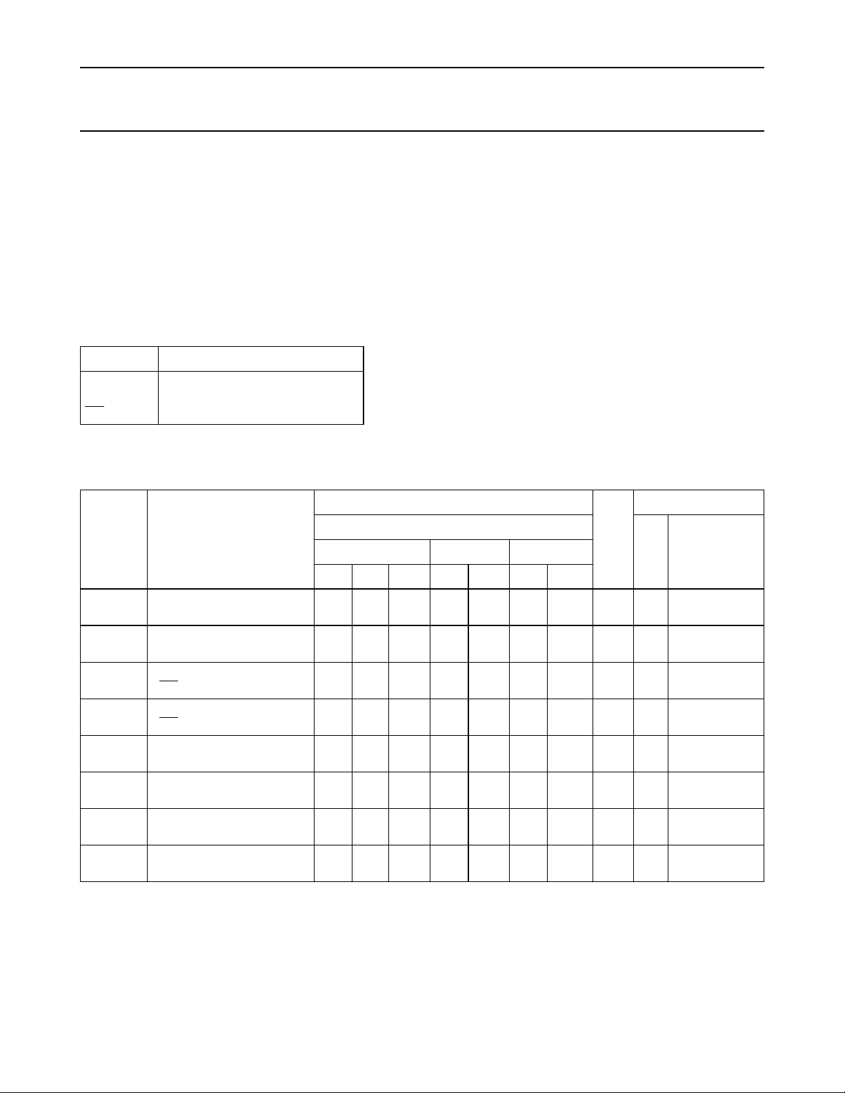
AC CHARACTERISTICS FOR 74HCT
GND = 0 V; t
= 6 ns; CL=50pF
r=tf
T
amb
(°C)
TEST CONDITIONS
74HCT
SYMBOL PARAMETER
+25 −40 to +85 −40 to +125
UNIT
V
(V)
min. typ. max. min. max. min. max.
t
PHL
t
PHL
t
PZH
t
PHZ
t
THL
/ t
/ t
/ t
/ t
/ t
propagation delay
PLH
Dn to Q
propagation delay
PLH
LE to Q
3-state output enable time
PZL
OE to Q
3-state output disable time
PLZ
OE to Q
output transition time 5 12 15 18 ns 4.5 Fig.7
TLH
n
n
n
n
17 30 38 45 ns 4.5 Fig.7
16 32 40 48 ns 4.5 Fig.8
19 32 40 48 ns 4.5 Fig.9
18 30 38 45 ns 4.5 Fig.9
WAVEFORMS
CC
t
W
LE pulse width
16 4 20 24 ns 4.5 Fig.8
HIGH
t
su
set-up time
12 6 15 18 ns 4.5 Fig.10
Dn to LE
t
h
hold time
4 −1 4 4 ns 4.5 Fig.10
Dn to LE
September 1993 6
Page 7
Philips Semiconductors Product specification
Octal D-type transparent latch; 3-state 74HC/HCT373
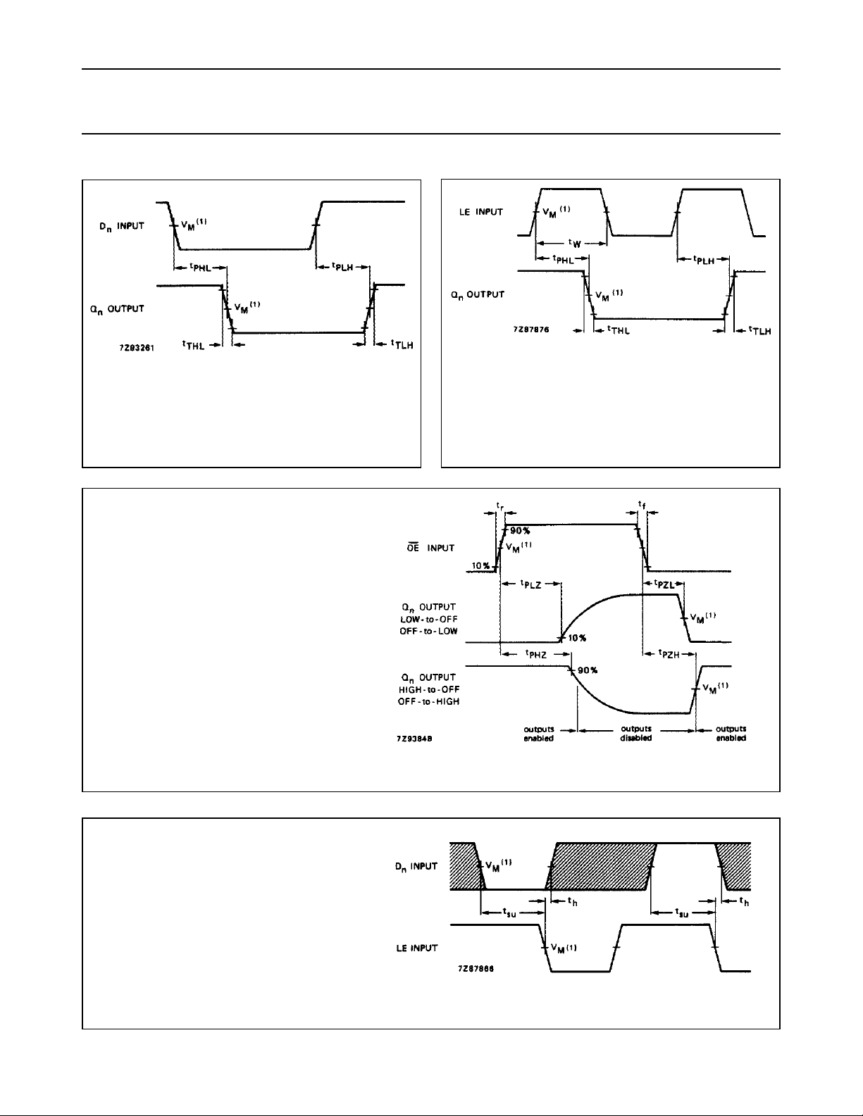
AC WAVEFORMS
(1) HC : VM= 50%; VI= GND to VCC.
HCT : V
= 1.3 V; VI= GND to 3 V.
M
Fig.7 Waveforms showing the input (Dn) to output
(Qn) propagation delays and the output
transition times.
(1) HC : VM= 50%; VI= GND to VCC.
HCT : V
= 1.3 V; VI= GND to 3 V.
M
(1) HC : VM= 50%; VI= GND to VCC.
HCT : V
= 1.3 V; VI= GND to 3 V.
M
Fig.8 Waveforms showing the latch enable input
(LE) pulse width, the latch enable input to
output (Qn) propagation delays and the
output transition times.
Fig.9 Waveforms showing the 3-state enable and disable times.
The shaded areas indicate when the input is permitted to
change for predictable output performance.
(1) HC : V
HCT : V
= 50%; VI= GND to VCC.
M
= 1.3 V; VI= GND to 3 V.
M
Fig.10 Waveforms showing the data set-up and hold times for Dn input to LE input.
September 1993 7
Page 8

Philips Semiconductors Product specification
Octal D-type transparent latch; 3-state 74HC/HCT373
PACKAGE OUTLINES
See
“74HC/HCT/HCU/HCMOS Logic Package Outlines”
.
September 1993 8
 Loading...