

Page 1
INTEGRATED CIRCUITS
DATA SH EET
For a complete data sheet, please also download:
•The IC06 74HC/HCT/HCU/HCMOS Logic Family Specifications
•The IC06 74HC/HCT/HCU/HCMOS Logic Package Information
•The IC06 74HC/HCT/HCU/HCMOS Logic Package Outlines
74HC/HCT32
Quad 2-input OR gate
Product specification
File under Integrated Circuits, IC06
December 1990
Page 2
Philips Semiconductors Product specification
Quad 2-input OR gate 74HC/HCT32
FEATURES
• Output capability: standard
• ICC category: SSI
GENERAL DESCRIPTION
The 74HC/HCT32 are high-speed Si-gate CMOS devices
and are pin compatible with low power Schottky TTL
(LSTTL). They are specified in compliance with JEDEC
standard no. 7A.
The 74HC/HCT32 provide the 2-input OR function.
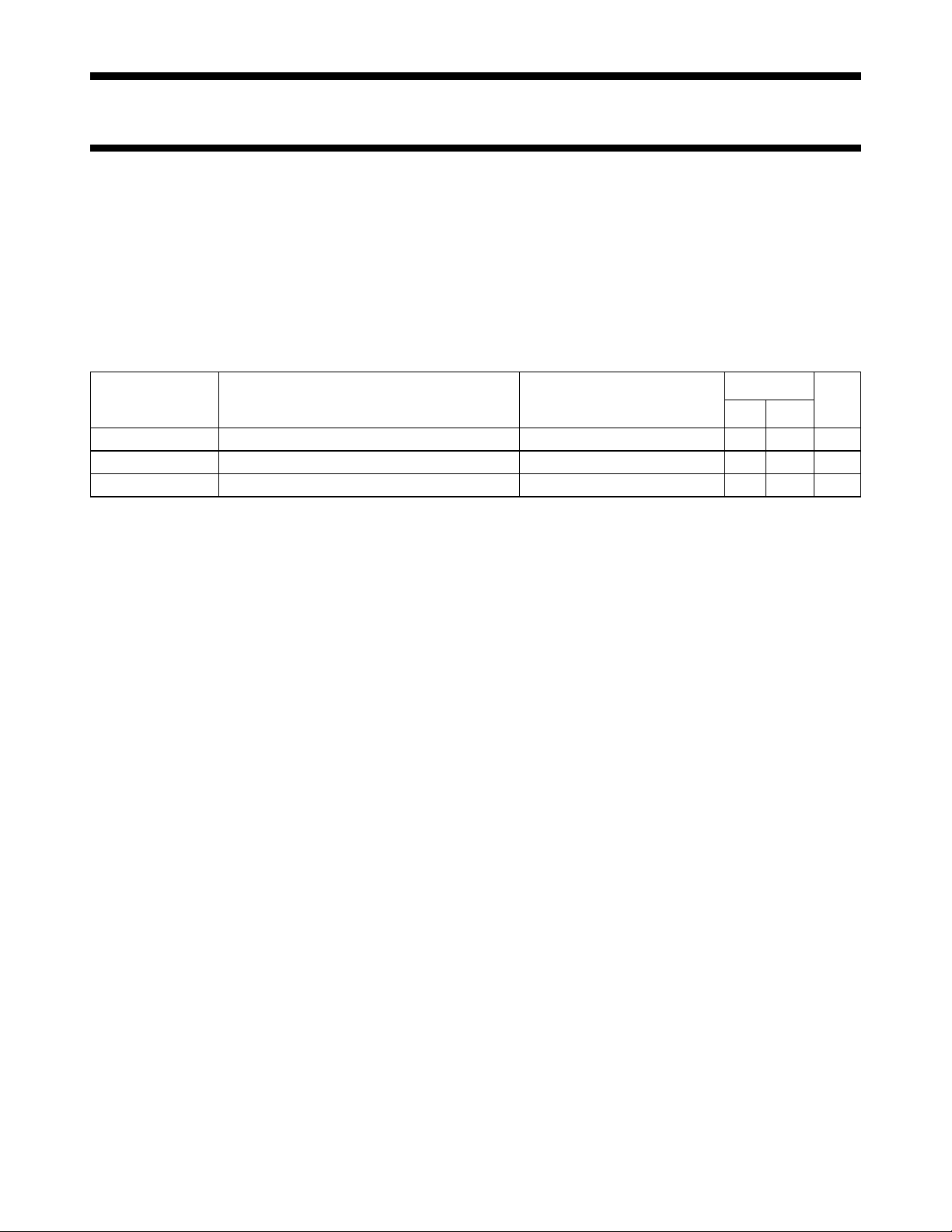
QUICK REFERENCE DATA
GND = 0 V; T
=25°C; tr=tf=6ns
amb
SYMBOL PARAMETER CONDITIONS
t
PHL
C
C
I
PD
/ t
PLH
propagation delay nA, nB to nY CL = 15 pF; VCC=5V 6 9 ns
input capacitance 3.5 3.5 pF
power dissipation capacitance per gate notes 1 and 2 16 28 pF
Notes
1. C
is used to determine the dynamic power dissipation (PD in µW):
PD
PD=CPD× V
2
× fi+∑(CL× V
CC
2
× fo) where:
CC
fi= input frequency in MHz
fo= output frequency in MHz
∑ (CL× V
2
× fo) = sum of outputs
CC
CL= output load capacitance in pF
VCC= supply voltage in V
2. For HC the condition is VI= GND to V
CC
For HCT the condition is VI= GND to VCC− 1.5 V
TYPICAL
UNIT
HC HCT
ORDERING INFORMATION
“74HC/HCT/HCU/HCMOS Logic Package Information”
See
December 1990 2
.
Page 3
Philips Semiconductors Product specification
Quad 2-input OR gate 74HC/HCT32
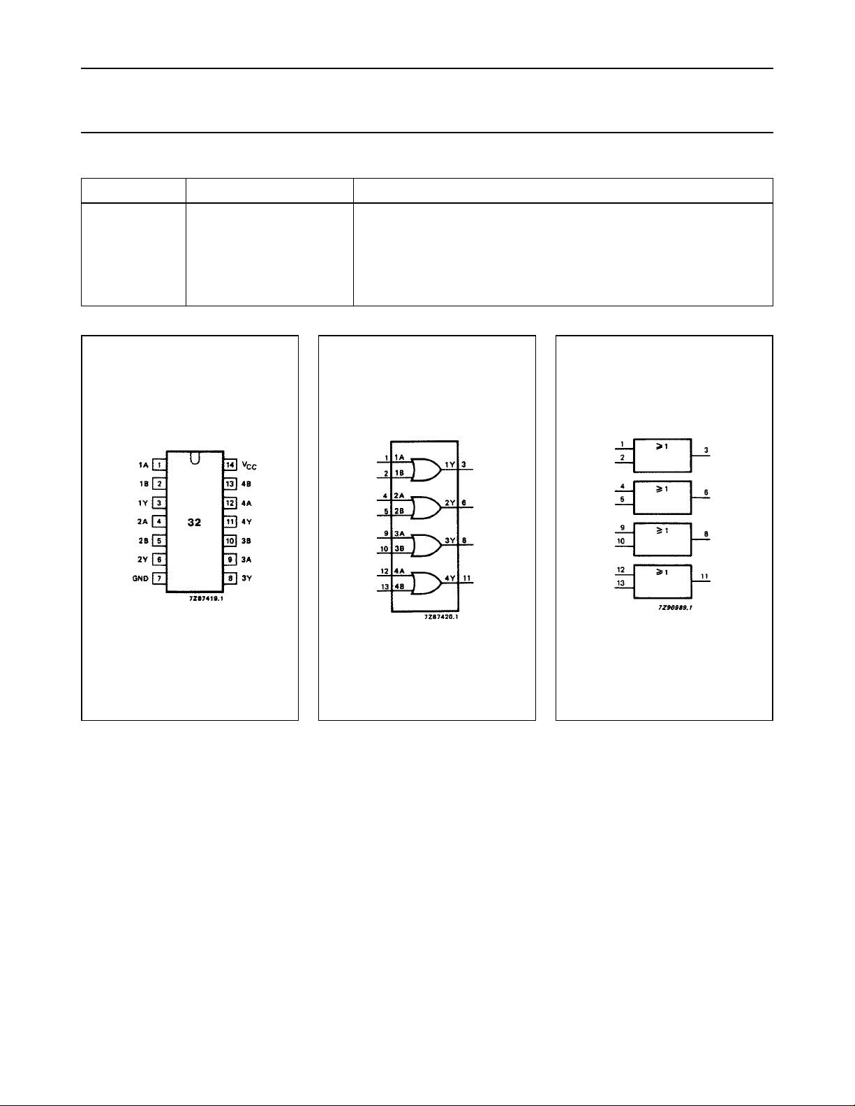
PIN DESCRIPTION
PIN NO. SYMBOL NAME AND FUNCTION
1, 4, 9, 12 1A to 4A data inputs
2, 5, 10, 13 1B to 4B data inputs
3, 6, 8, 11 1Y to 4Y data outputs
7 GND ground (0 V)
14 V
CC
positive supply voltage
Fig.1 Pin configuration. Fig.2 Logic symbol. Fig.3 IEC logic symbol.
December 1990 3
Page 4
Philips Semiconductors Product specification
Quad 2-input OR gate 74HC/HCT32
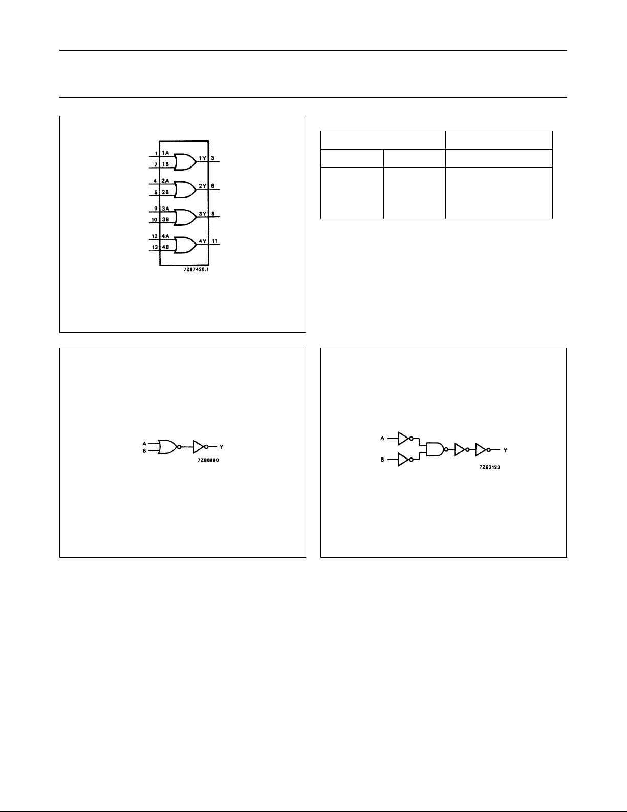
FUNCTION TABLE
INPUTS OUTPUT
nA nB nY
L
L
H
H
Notes
1. H = HIGH voltage level
L = LOW voltage level
Fig.4 Functional diagram.
L
H
L
H
L
H
H
H
Fig.5 Logic diagram 74HC (one gate). Fig.6 Logic diagram 74HCT (one gate).
December 1990 4
Page 5
Philips Semiconductors Product specification
Quad 2-input OR gate 74HC/HCT32
DC CHARACTERISTICS FOR 74HC
For the DC characteristics see
“74HC/HCT/HCU/HCMOS Logic Family Specifications”
Output capability: standard
ICC category: SSI
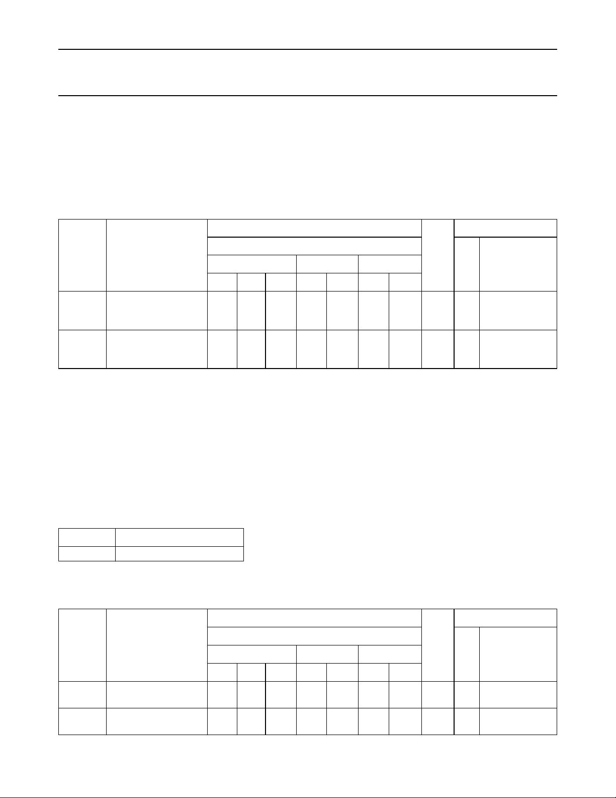
AC CHARACTERISTICS FOR 74HC
GND = 0 V; t
= 6 ns; CL=50pF
r=tf
SYMBOL PARAMETER
min. typ. max. min. max. min. max.
t
PHL
/ t
propagation delay
PLH
nA, nB to nY
t
THL
/ t
output transition time 19
TLH
DC CHARACTERISTICS FOR 74HCT
For the DC characteristics see
“74HC/HCT/HCU/HCMOS Logic Family Specifications”
T
(°C)
amb
74HC
+25 −40 to +85 −40 to +125
22
90
8
18
6
15
75
7
15
6
13
115
23
20
95
19
16
135
27
23
110
22
19
.
UNIT
ns 2.0
ns 2.0
.
TEST CONDITIONS
WAVEFORMS
V
CC
(V)
Fig.7
4.5
6.0
Fig.7
4.5
6.0
Output capability: standard
ICC category: SSI
Note to HCT types
The value of additional quiescent supply current (∆I
) for a unit load of 1 is given in the family specifications.
CC
To determine ∆ICC per input, multiply this value by the unit load coefficient shown in the table below.
INPUT UNIT LOAD COEFFICIENT
nA, nB 1.20
AC CHARACTERISTICS FOR 74HCT
GND = 0 V; t
SYMBOL PARAMETER
= 6 ns; CL=50pF
r=tf
T
(°C)
amb
74HCT
+25 −40 to +85 −40 to +125
UNIT
TEST CONDITIONS
V
CC
(V)
min. typ. max. min. max. min. max.
t
PHL
/ t
propagation delay
PLH
11 24 30 36 ns 4.5 Fig.7
nA, nB to nY
t
THL
/ t
output transition time 7 15 19 22 ns 4.5 Fig.7
TLH
WAVEFORMS
December 1990 5
Page 6
Philips Semiconductors Product specification
Quad 2-input OR gate 74HC/HCT32
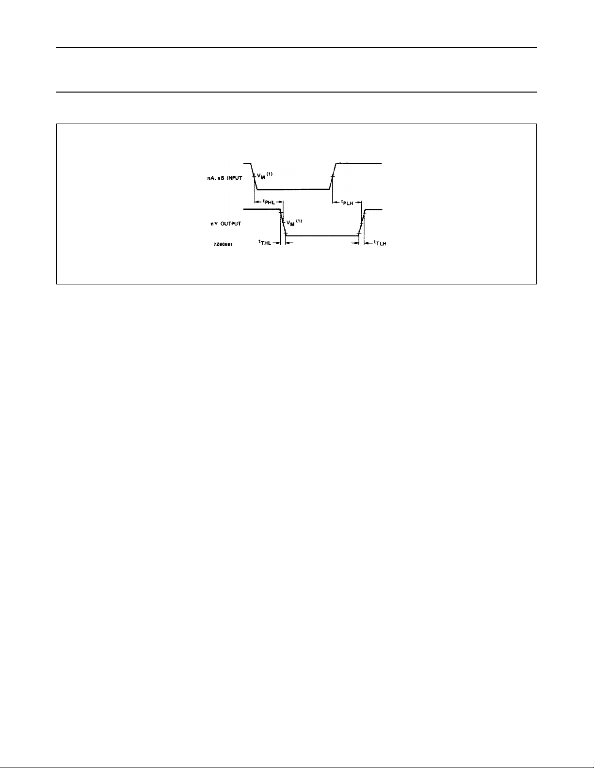
AC WAVEFORMS
(1) HC : VM= 50%; VI= GND to VCC.
= 1.3 V; VI= GND to 3 V.
HCT: V
M
Fig.7 Waveforms showing the input (nA, nB) to output (nY) propagation delays and the output transition times.
PACKAGE OUTLINES
“74HC/HCT/HCU/HCMOS Logic Package Outlines”
See
.
December 1990 6
 Loading...