

Page 1
INTEGRATED CIRCUITS
DATA SH EET
For a complete data sheet, please also download:
•The IC06 74HC/HCT/HCU/HCMOS Logic Family Specifications
•The IC06 74HC/HCT/HCU/HCMOS Logic Package Information
•The IC06 74HC/HCT/HCU/HCMOS Logic Package Outlines
74HC/HCT297
Digital phase-locked-loop filter
Product specification
File under Integrated Circuits, IC06
September 1993
Page 2

Philips Semiconductors Product specification
Digital phase-locked-loop filter 74HC/HCT297
FEATURES
• Digital design avoids analog compensation errors
• Easily cascadable for higher order loops
• Useful frequency range:
– DC to 55 MHz typical (K-clock)
– DC to 35 MHz typical (I/D-clock)
• Dynamically variable bandwidth
• Very narrow bandwidth attainable
• Power-on reset
• Output capability: standard/bus driver
• ICC category: MSI
GENERAL DESCRIPTION
The 74HC/HCT297 are high-speed Si-gate CMOS devices
and are pin compatible with low power Schottky TTL
(LSTTL). They are specified in compliance with JEDEC
standard no. 7A.
The 74HC/HCT297 are designed to provide a simple,
cost-effective solution to high-accuracy, digital,
phase-locked-loop applications. These devices contain all
the necessary circuits, with the exception of the
divide-by-n counter, to build first order
phase-locked-loops.
Both EXCLUSIVE-OR (XORPD) and edge-controlled
(ECPD) phase detectors are provided for maximum
flexibility. The input signals for the EXCLUSIVE-OR phase
detector must have a 50% duty factor to obtain the
maximum lock-range.
Proper partitioning of the loop function, with many of the
building blocks external to the package, makes it easy for
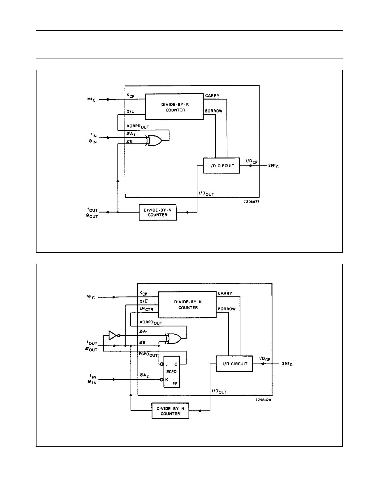
the designer to incorporate ripple cancellation (see Fig.7)
or to cascade to higher order phase-locked-loops.
The length of the up/down K-counter is digitally
programmable according to the K-counter function table.
With, A, B, C and D all LOW, the K-counter is disabled.
With A HIGH and B, C and D LOW, the K-counter is only
three stages long, which widens the bandwidth or capture
range and shortens the lock time of the loop. When A, B,
C and D are all programmed HIGH, the K-counter
becomes seventeen stages long, which narrows the
bandwidth or capture range and lengthens the lock time.
Real-time control of loop bandwidth by manipulating the A
to D inputs can maximize the overall performance of the
digital phase-locked loop.
The “297” can perform the classic first-order
phase-locked-loop function without using analog
components. The accuracy of the digital
phase-locked-loop (DPLL) is not affected by V
CC
and
temperature variations but depends solely on accuracies
of the K-clock, I/D-clock and loop propagation delays.
The phase detector generates an error signal waveform
that, at zero phase error, is a 50% duty factor square wave.
At the limits of linear operation, the phase detector output
will be either HIGH or LOW all of the time depending on the
− φ
direction of the phase error (φ
IN
). Within these limits
OUT
the phase detector output varies linearly with the input
phase error according to the gain k
, which is expressed in
d
terms of phase detector output per cycle or phase error.
The phase detector output can be defined to vary between
± 1 according to the relation:
phase detector output
% HIGH % LOW–
------------------------------------------------
The output of the phase detector will be k
phase error φ
= φIN−φ
e
OUT
.
˙˙
100
, where the
dφe
.=
EXCLUSIVE-OR phase detectors (XORPD) and
edge-controlled phase detectors (ECPD) are commonly
used digital types. The ECPD is more complex than the
XORPD logic function but can be described generally as a
circuit that changes states on one of the transitions of its
inputs. The gain (k
remains HIGH (XORPD
) for an XORPD is 4 because its output
d
= 1) for a phase error of 1/4
OUT
cycle.
Similarly, k
for the ECPD is 2 since its output remains
d
HIGH for a phase error of 1/2 cycle. The type of phase
detector will determine the zero-phase-error point, i.e., the
phase separation of the phase detector inputs for a
φ
defined to be zero. For the basic DPLL system of
e
Fig.6 φ
= 0 when the phase detector output is a square
e
wave.
The XORPD inputs are 1/4 cycle out-of-phase for zero
phase error. For the ECPD, φ
= 0 when the inputs are 1/2
e
cycle out-of-phase.
The phase detector output controls the up/down input to
the K-counter. The counter is clocked by input frequency
Mfc, which is a multiple M of the loop centre frequency fc.
When the K-counter recycles up, it generates a carry
pulse. Recycling while counting down generates a borrow
pulse. If the carry and the borrow outputs are conceptually
combined into one output that is positive for a carry and
negative for a borrow, and if the K-counter is considered as
a frequency divider with the ratio Mfc/K, the output of the
K-counter will equal the input frequency multiplied by the
division ratio. Thus the output from the K-counter is
(kdφeMfc) / K.
September 1993 2
Page 3
Philips Semiconductors Product specification
Digital phase-locked-loop filter 74HC/HCT297
The carry and borrow pulses go to the
increment/decrement (I/D) circuit which, in the absence of
any carry or borrow pulses has an output that is 1/2 of the
input clock (I/DCP). The input clock is just a multiple, 2N, of
the loop centre frequency. In response to a carry or borrow
pulse, the I/D circuit will either add or delete a pulse at
I/D
. Thus the output of the I/D circuit will be
OUT
Nfc+ (kd∅eMfc)/2K.
The output of the N-counter (or the output of the
phase-locked-loop) is thus: fo=fc+(kdφeMfc)/2KN.
If this result is compared to the equation for a first-order
analog phase-locked-loop, the digital equivalent of the
gain of the VCO is just Mfc/2KN or fc/K for M = 2N.
Thus the simple first-order phase-locked-loop with an
adjustable K-counter is the equivalent of an analog
phase-locked-loop with a programmable VCO gain.
QUICK REFERENCE DATA
GND = 0 V; T
=25°C; tr=tf= 6 ns
amb
SYMBOL PARAMETER CONDITIONS
t
PHL/ tPLH
f
max
C
I
C
PD
propagation delay CL= 15 pF; VCC=5 V
I/D
to I/D
CP
, φB to XORPD
φA
1
φB, φA
OUT
to ECPD
2
OUT
OUT
maximum clock frequency
K
CP
I/D
CP
input capacitance 3.5 3.5 pF
power dissipation capacitance per package notes 1 and 2 18 19 pF
TYPICAL
UNIT
HC HCT
15 18 ns
13 13 ns
19 19 ns
63 68 MHz
41 40 MHz
Notes
1. C
is used to determine the dynamic power dissipation (PD in µW):
PD
PD=CPD× V
2
× fi+ ∑ (CL× V
CC
2
× fo) where:
CC
fi= input frequency in MHz
fo= output frequency in MHz
∑ (CL× V
2
× fo) = sum of outputs
CC
CL= output load capacitance in pF
VCC= supply voltage in V
2. For HC the condition is VI= GND to V
CC
For HCT the condition is VI= GND to VCC− 1.5 V
ORDERING INFORMATION
“74HC/HCT/HCU/HCMOS Logic Package Information”
See
.
September 1993 3
Page 4
Philips Semiconductors Product specification
Digital phase-locked-loop filter 74HC/HCT297
PIN DESCRIPTION
PIN NO. SYMBOL NAME AND FUNCTION
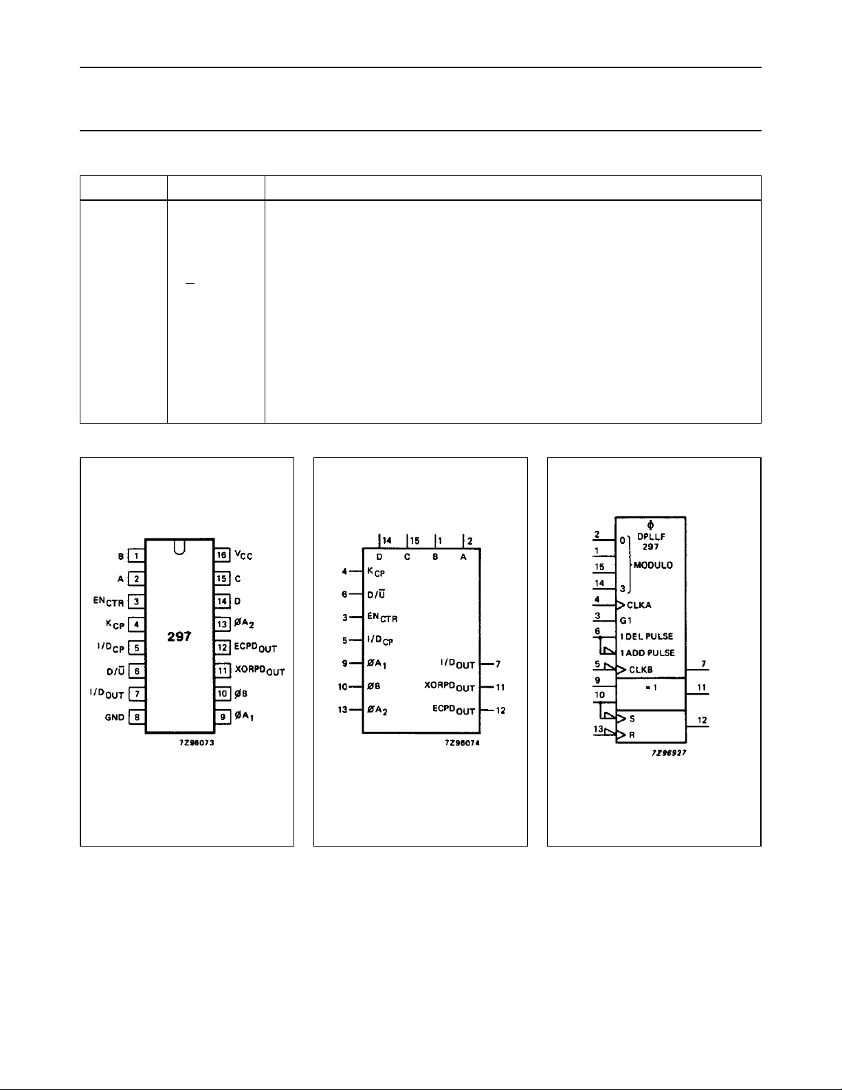
2, 1, 15, 14 A, B, C, D modulo control inputs
3EN
4K
5 I/D
6D/
7 I/D
CTR
CP
CP
U down/up control
OUT
8 GND ground (0 V)
9, 10, 13 φA
11 XORPD
12 ECPD
16 V
, φB, φA
1
CC
OUT
OUT
K-counter enable input
K-counter clock input (LOW-to-HIGH, edge-triggered)
increment/decrement clock input (HIGH-to-LOW, edge-triggered)
increment/decrement bus output
phase inputs
2
EXCLUSIVE-OR phase detector output
edge-controlled phase detector output
positive supply voltage
Fig.1 Pin configuration. Fig.2 Logic symbol. Fig.3 IEC logic symbol.
September 1993 4
Page 5
Philips Semiconductors Product specification
Digital phase-locked-loop filter 74HC/HCT297
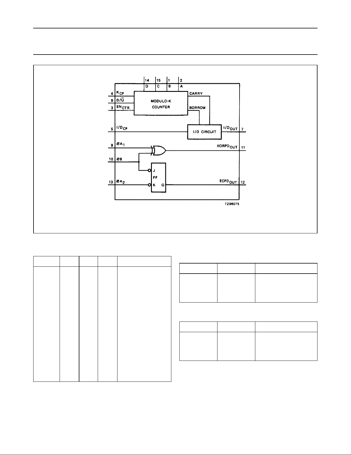
Fig.4 Functional diagram.
K-COUNTER (DIGITAL CONTROL) FUNCTION TABLE
D C B A MODULO (K)
L
L
L
L
L
L
L
L
H
H
H
H
H
H
H
H
L
L
L
L
H
H
H
H
L
L
L
L
H
H
H
H
L
L
H
H
L
L
H
H
L
L
H
H
L
L
H
H
L
H
L
H
L
H
L
H
L
H
L
H
L
H
L
H
inhibited
3
2
4
2
5
2
6
2
7
2
8
2
9
2
10
2
11
2
12
2
13
2
14
2
15
2
16
2
17
2
EXCLUSIVE-OR PHASE DETECTOR FUNCTION TABLE
φA
1
L
L
H
H
φB XORPD
L
H
L
H
L
H
H
L
OUT
EDGE-CONTROLLED PHASE DETECTOR TABLE
H or L
↓
H or L
↑
φA
2
φB ECPD
↓
H or L
↑
H or L
H
L
no change
no change
OUT
Notes
1. H = HIGH voltage level
L = LOW voltage level
↓ = HIGH-to-LOW transition
↑ = LOW-to-HIGH transition
September 1993 5
Page 6
Philips Semiconductors Product specification
Digital phase-locked-loop filter 74HC/HCT297
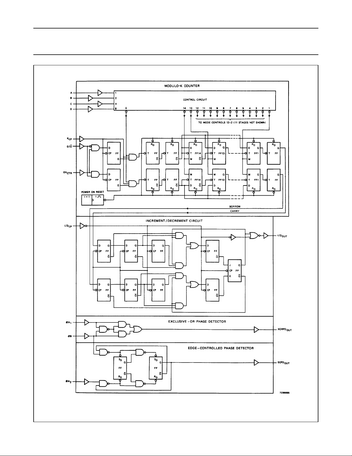
Fig.5 Logic diagram.
September 1993 6
Page 7
Philips Semiconductors Product specification
Digital phase-locked-loop filter 74HC/HCT297
Fig.6 DPLL using EXCLUSIVE-OR phase detection.
Fig.7 DPLL using both phase detectors in a ripple-cancellation scheme.
September 1993 7
Page 8
Philips Semiconductors Product specification
Digital phase-locked-loop filter 74HC/HCT297
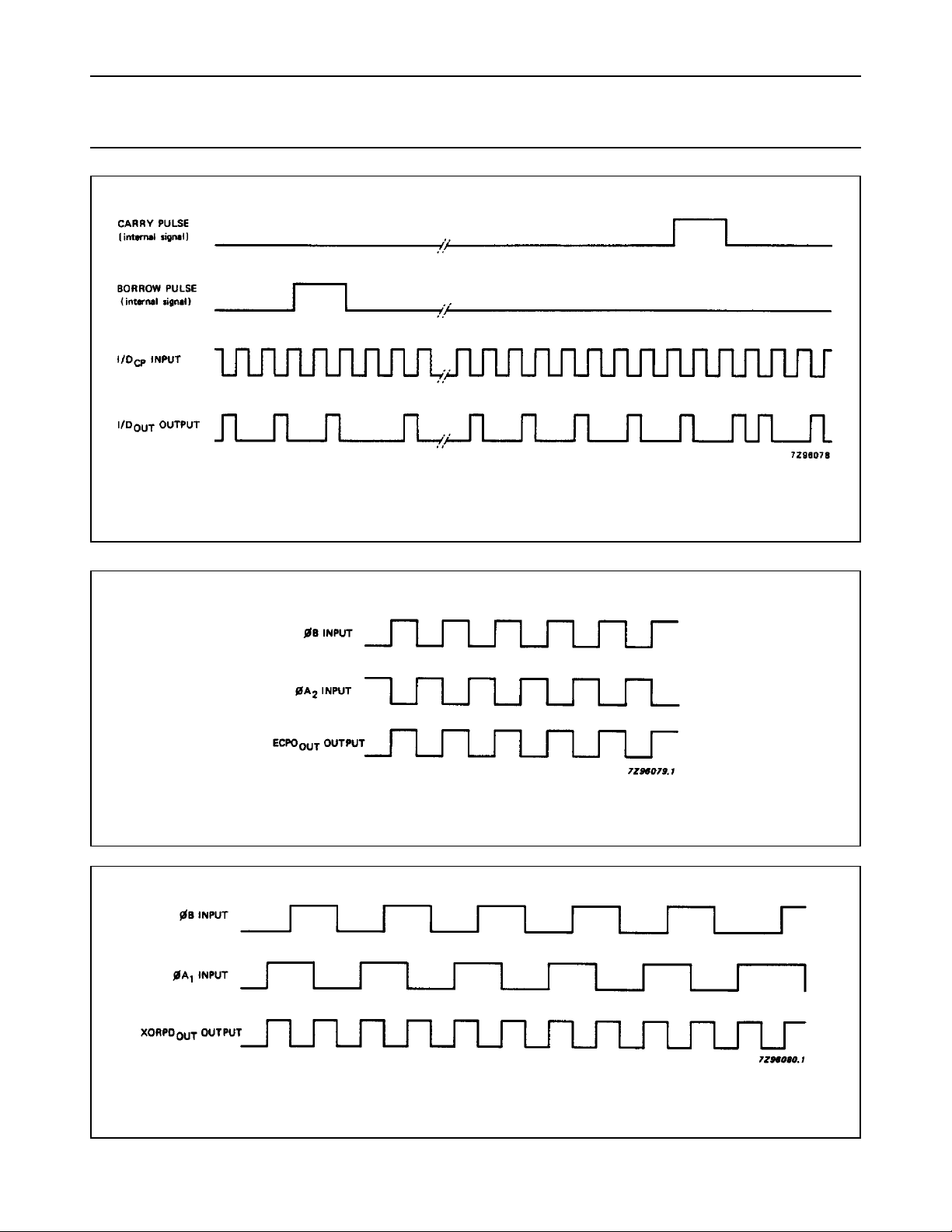
Fig.8 Timing diagram: I/D
Fig.9 Timing diagram: edge-controlled phase comparator waveforms.
in-lock condition.
OUT
Fig.10 Timing diagram: EXCLUSIVE-OR phase detector waveforms.
September 1993 8
Page 9
Philips Semiconductors Product specification
Digital phase-locked-loop filter 74HC/HCT297
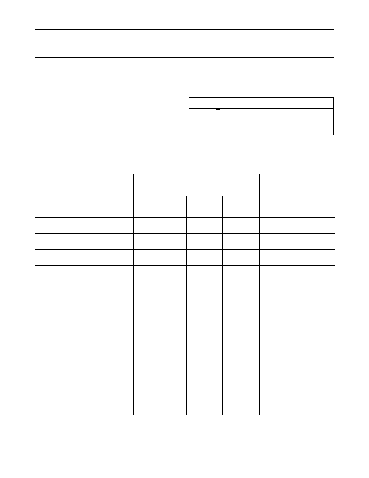
DC CHARACTERISTICS FOR 74HC
For the DC characteristics see
“74HC/HCT/HCU/HCMOS Logic Family Specifications”
Output capability: standard/bus driver
ICC category: MSI
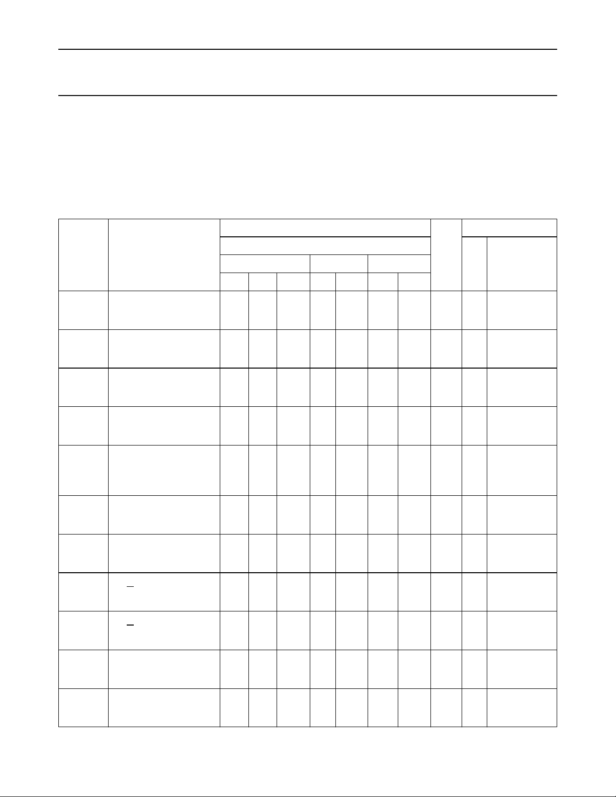
AC CHARACTERISTICS FOR 74HC
GND = 0 V; t
= 6 ns; CL= 50 pF
r=tf
SYMBOL PARAMETER
t
PHL
t
PHL
/ t
/ t
propagation delay
PLH
I/DCP to I/D
propagation delay
PLH
OUT
φA1, φB
t
PHL
t
THL
to XORPD
/ t
propagation delay
PLH
φB, φA
to ECPD
/ t
output transition time:
TLH
OUT
2
OUT
bus driver output;
I/D
(pin 7)
OUT
t
THL
/ t
output transition time:
TLH
standard outputs;
XORPD
OUT
, ECPD
OUT
(pins 11, 12)
t
W
t
W
t
su
t
h
f
max
f
max
clock pulse width
K
CP
clock pulse width
I/D
CP
set-up time
D/U, EN
CTR
to K
CP
hold time
D/U, EN
CTR
to K
CP
maximum clock pulse
frequency K
CP
maximum clock pulse
frequency I/D
CP
(°C)
T
amb
74HC
+25 −40 to +85 −40 to +125
min. typ. max. min. max. min. max.
50
80
16
14
100
20
17
120
24
20
0
0
0
6.0
30
35
4.0
20
24
18
14
44
16
13
61
22
18
14
5
4
19
7
6
22
8
6
28
10
8
33
12
10
−19
−7
−6
19
57
68
12
37
44
175
35
30
160
32
27
220
44
37
60
12
10
75
15
13
100
20
17
125
25
21
150
30
26
0
0
0
4.8
24
28
3.2
16
19
220
44
37
200
40
34
275
55
47
75
15
13
95
19
16
265
53
45
240
48
41
330
66
56
90
18
15
110
22
19
120
24
20
150
30
26
180
36
31
0
0
0
4.0
20
24
2.6
13
15
.
UNIT
ns 2.0
ns 2.0
ns 2.0
ns 2.0
ns 2.0
ns 2.0
ns 2.0
ns 2.0
ns 2.0
MHz 2.0
MHz 2.0
TEST CONDITIONS
WAVEFORMS
V
CC
(V)
Fig.11
4.5
6.0
Fig.12
4.5
6.0
Fig.13
4.5
6.0
Fig.11
4.5
6.0
Fig.12 and 13
4.5
6.0
Fig.14
4.5
6.0
Fig.11
4.5
6.0
Fig.14
4.5
6.0
Fig.14
4.5
6.0
Fig.14
4.5
6.0
Fig.11
4.5
6.0
September 1993 9
Page 10
Philips Semiconductors Product specification
Digital phase-locked-loop filter 74HC/HCT297
DC CHARACTERISTICS FOR 74HCT
For the DC characteristics see
“74HC/HCT/HCU/HCMOS Logic Family Specifications”
Output capability: standard/bus driver
ICC category: MSI
Note to HCT types
The value of additional quiescent supply current (∆I
CC
) for
a unit load of 1 is given in the family specifications.
AC CHARACTERISTICS FOR 74HCT
GND = 0 V, t
= 6 ns; CL= 50 pF
r=tf
SYMBOL PARAMETER
+25 −40 to +85 −40 to +125
min. typ. max. min. max. min. max.
t
PHL
t
PHL
t
PHL
t
THL
/ t
/ t
/ t
/ t
propagation delay
PLH
I/DCP to I/D
propagation delay
PLH
φA1, φB to XORPD
propagation delay
PLH
φB, φA2 to ECPD
output transition time
TLH
21 35 44 53 ns 4.5 Fig.11
OUT
16 32 40 48 ns 4.5 Fig.12
OUT
22 44 55 66 ns 4.5 Fig.13
OUT
5 12 15 18 ns 4.5 Fig.11
bus driver output
I/D
(pin 7)
OUT
t
THL
/ t
output transition time
TLH
7 15 19 22 ns 4.5 Figs 12 and 13
standard outputs
XORPD
OUT
, ECPD
OUT
(pins 11, 12)
t
W
t
W
t
su
t
h
f
max
f
max
clock pulse width
K
CP
clock pulse width
I/D
CP
set-up time
D/U, EN
CTR
to K
CP
hold time
D/U, EN
CTR
to K
CP
maximum clock pulse
frequency K
CP
maximum clock pulse
frequency I/D
CP
16 8 20 24 ns 4.5 Fig.14
25 13 31 38 ns 4.5 Fig.11
24 13 30 36 ns 4.5 Fig.14
0 −8 0 0 ns 4.5 Fig.14
30 62 24 20 MHz 4.5 Fig.14
20 36 16 13 MHz 4.5 Fig.11
To determine ∆ICC per input, multiply this value by the unit
load coefficient shown in the table below.
.
INPUT UNIT LOAD COEFFICIENT
EN
, D/U 0.3
CTR
A, B, C, D, K
, φA1, φB 1.5
I/D
CP
(°C)
T
amb
CP,φA2
0.6
TEST CONDITIONS
74HCT
UNIT
WAVEFORMS
V
CC
(V)
September 1993 10
Page 11
Philips Semiconductors Product specification
Digital phase-locked-loop filter 74HC/HCT297
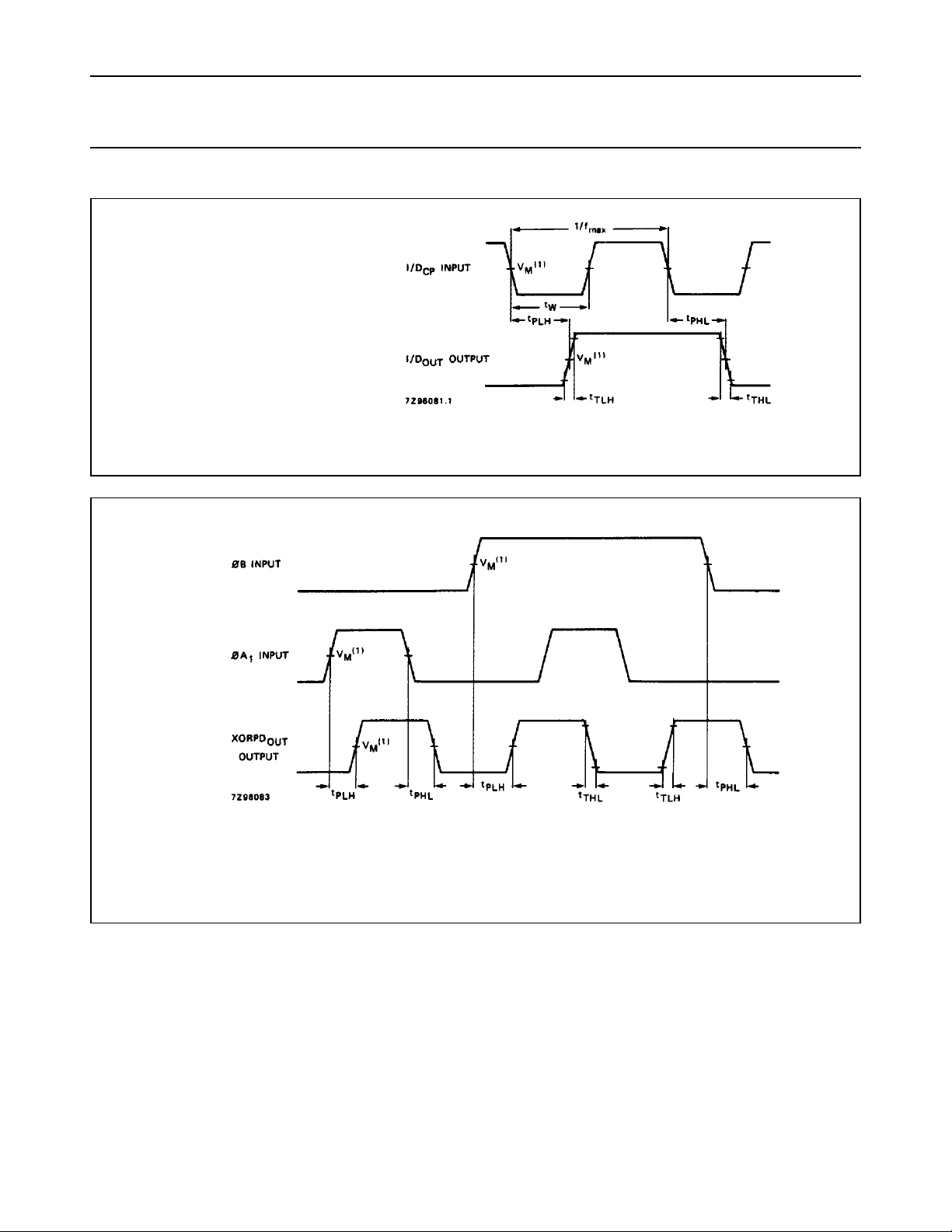
AC WAVEFORMS
(1) HC : VM= 50%; VI= GND to VCC.
= 1.3 V; VI= GND to 3 V.
HCT: V
M
Fig.11 Waveforms showing the clock (I/DCP) to output (I/D
transition times and maximum clock pulse frequency.
(1) HC : VM= 50%; VI= GND to VCC.
= 1.3 V; VI= GND to 3 V.
HCT: V
M
) propagation delays, the clock pulse width, output
OUT
Fig.12 Waveforms showing the phase input (φB, φA1) to output (XORPD
transition times.
September 1993 11
) propagation delays and output
OUT
Page 12
Philips Semiconductors Product specification
Digital phase-locked-loop filter 74HC/HCT297
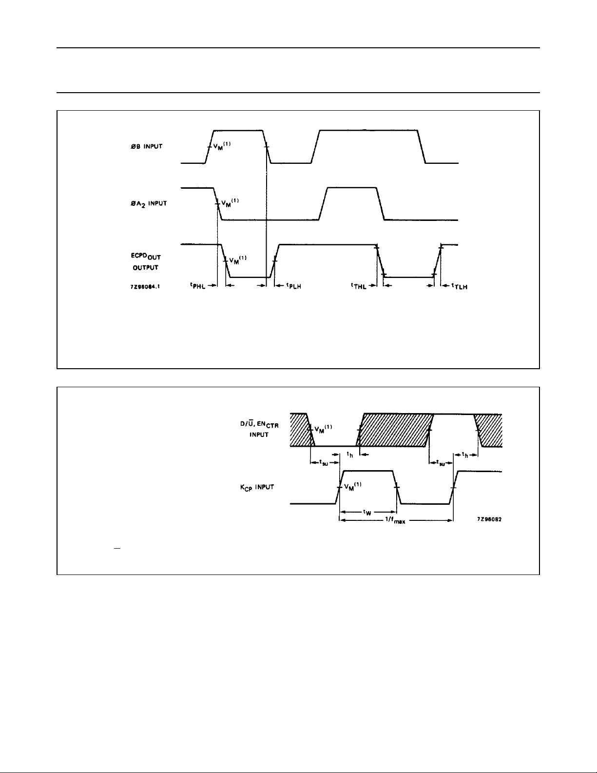
(1) HC : VM= 50%; VI= GND to VCC.
Fig.13 Waveforms showing the phase input (φB, φA2) to output (ECPD
= 1.3 V; VI= GND to 3 V.
HCT: V
M
) propagation delays and output
OUT
transition times.
The shaded areas indicate when the input is
permitted to change for predictable output
performance.
(1) HC : V
= 50%; VI= GND to VCC.
M
= 1.3 V; VI= GND to 3 V.
HCT: V
M
Fig.14 Waveforms showing the clock (KCP) pulse width and the maximum clock pulse frequency, and the input
(D/U, EN
) to clock (KCP) set-up and hold times.
CTR
PACKAGE OUTLINES
See
“74HC/HCT/HCU/HCMOS Logic Package Outlines”
.
September 1993 12
 Loading...