

Page 1
INTEGRATED CIRCUITS
DATA SH EET
For a complete data sheet, please also download:
•The IC06 74HC/HCT/HCU/HCMOS Logic Family Specifications
•The IC06 74HC/HCT/HCU/HCMOS Logic Package Information
•The IC06 74HC/HCT/HCU/HCMOS Logic Package Outlines
74HC/HCT280
9-bit odd/even parity
generator/checker
Product specification
File under Integrated Circuits, IC06
December 1990
Page 2
Philips Semiconductors Product specification
9-bit odd/even parity generator/checker 74HC/HCT280
FEATURES
• Word-length easily expanded by cascading
• Similar pin configuration to the “180” for easy system
up-grading
• Generates either odd or even parity for nine data bits
• Output capability: standard
• ICC category: MSI
transmission or data retrieval systems. Both even and odd
parity outputs are available for generating or checking
even or odd parity up to 9 bits.
The even parity output (∑
of data inputs (I0 to I8) are HIGH. The odd parity output (∑0)
is HIGH when an odd number of data inputs are HIGH.
Expansion to larger word sizes is accomplished by tying
the even outputs (∑E) of up to nine parallel devices to the
data inputs of the final stage. For a single-chip 16-bit
GENERAL DESCRIPTION
even/odd parity generator/checker, see
PC74HC/HCT7080.
The 74HC/HCT280 are high-speed Si-gate CMOS devices
and are pin compatible with low power Schottky TTL
(LSTTL). They are specified in compliance with JEDEC
standard no. 7A.
The 74HC/HCT280 are 9-bit parity generators or checkers
APPLICATIONS
• 25-line parity generator/checker
• 81-line parity generator/checker
commonly used to detect errors in high-speed data
QUICK REFERENCE DATA
GND = 0 V; T
=25°C; tr=tf= 6 ns
amb
SYMBOL PARAMETER CONDITIONS
t
PHL
C
C
/ t
I
PD
propagation delay CL= 15 pF; VCC=5 V
PLH
I
to ∑
n
E
I
to ∑
n
O
input capacitance 3.5 3.5 pF
power dissipationcapacitance per package notes 1 and 2 65 65 pF
) is HIGH when an even number
E
TYPICAL
UNIT
HC HCT
17 18 ns
20 22 ns
Notes
1. C
is used to determine the dynamic power dissipation (PD in µW):
PD
PD=CPD× V
2
× fi+∑(CL× V
CC
2
× fo) where:
CC
fi= input frequency in MHz
fo= output frequency in MHz
∑ (CL× V
2
× fo) = sum of outputs
CC
CL= output load capacitance in pF
VCC= supply voltage in V
2. For HC the condition is VI= GND to V
CC
For HCT the condition is VI= GND to VCC− 1.5 V
ORDERING INFORMATION
“74HC/HCT/HCU/HCMOS Logic Package Information”
See
December 1990 2
.
Page 3
Philips Semiconductors Product specification
9-bit odd/even parity generator/checker 74HC/HCT280
PIN DESCRIPTION
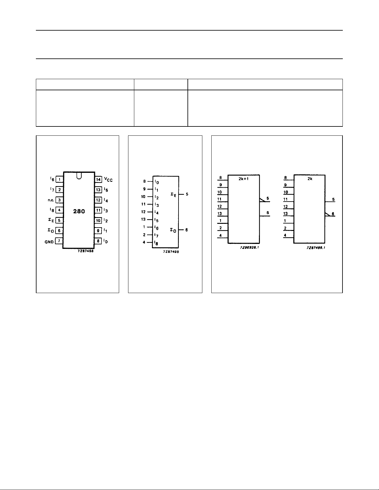
PIN NO. SYMBOL NAME AND FUNCTION
8, 9, 10, 11, 12, 13, 1, 2, 4 I
5, 6 ∑
7 GND ground (0 V)
14 V
to I
0
E
CC
, ∑
8
O
data inputs
parity outputs
positive supply voltage
Fig.1 Pin configuration. Fig.2 Logic symbol. Fig.3 IEC logic symbol.
December 1990 3
Page 4
Philips Semiconductors Product specification
9-bit odd/even parity generator/checker 74HC/HCT280
FUNCTION TABLE
INPUTS OUTPUTS
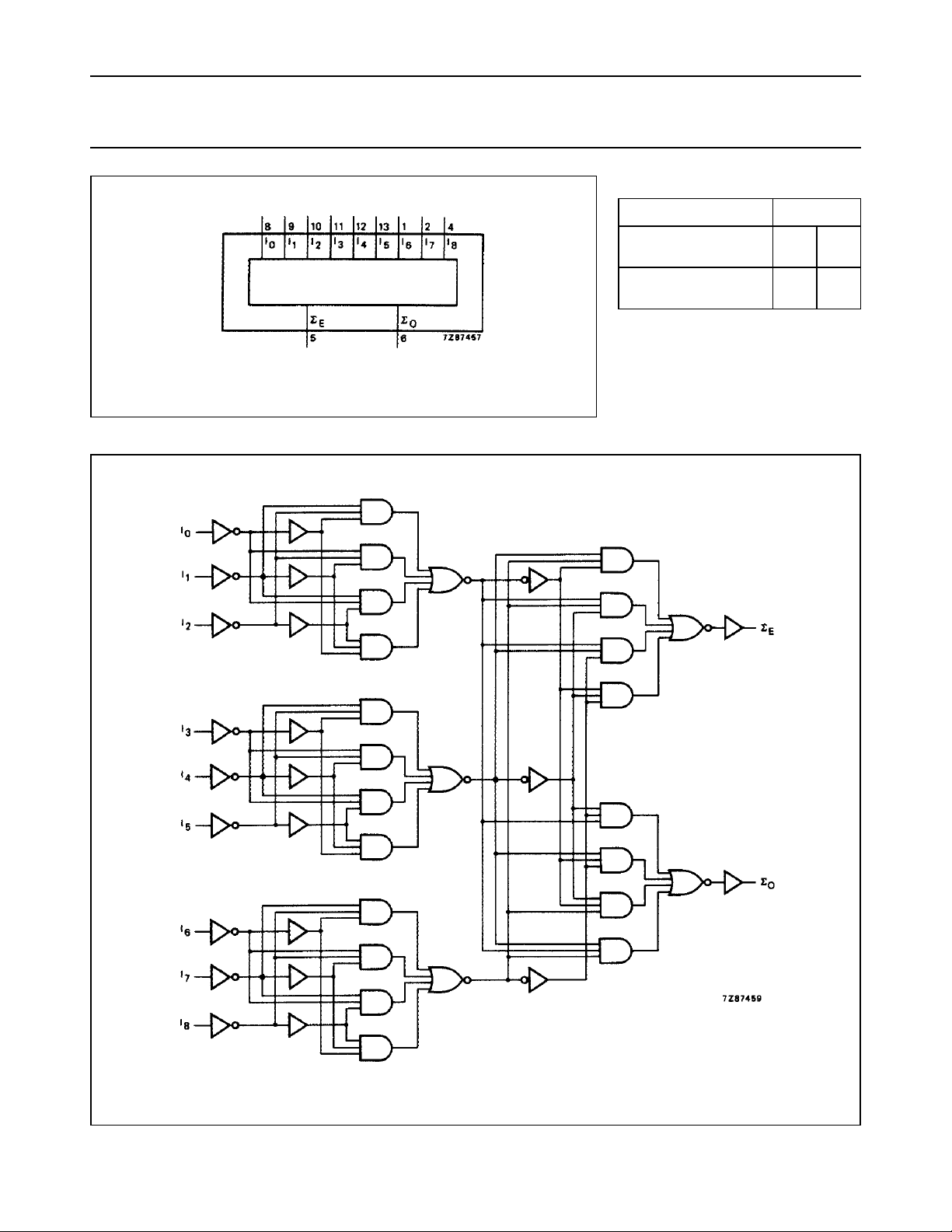
Fig.4 Functional diagram.
number of HIGH data
inputs (I
to I8)
0
even
odd
Note
1. H = HIGH voltage level
L = LOW voltage level
∑
∑
E
O
H
L
L
H
Fig.5 Logic diagram.
December 1990 4
Page 5
Philips Semiconductors Product specification
9-bit odd/even parity generator/checker 74HC/HCT280
DC CHARACTERISTICS FOR 74HC
For the DC characteristics see
“74HC/HCT/HCU/HCMOS Logic Family Specifications”
Out put capability: standard
ICC category: MSI
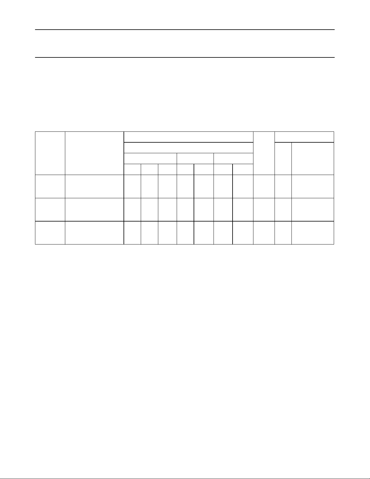
AC CHARACTERISTICS FOR 74HC
GND = 0 V; t
= 6 ns; CL= 50 pF
r=tf
SYMBOL PARAMETER
t
PHL
t
PHL
t
THL
/ t
/ t
/ t
propagation delay
PLH
In to ∑
E
propagation delay
PLH
In to ∑
O
output transition time 19
TLH
(°C)
T
amb
74HC
+25 −40 to +85 −40 to +125
min. typ. max. min. max. min. max.
55
20
16
63
23
18
7
6
200
40
34
200
40
34
75
15
13
250
50
43
250
50
43
95
19
16
300
60
51
300
60
51
110
22
19
.
UNIT
ns 2.0
ns 2.0
ns 2.0
TEST CONDITIONS
WAVEFORMS
V
CC
(V)
Fig.6
4.5
6.0
Fig.6
4.5
6.0
Fig.6
4.5
6.0
December 1990 5
Page 6
Philips Semiconductors Product specification
9-bit odd/even parity generator/checker 74HC/HCT280
DC CHARACTERISTICS FOR 74HCT
For the DC characteristics see
“74HC/HCT/HCU/HCMOS Logic Family Specifications”
.
Output capability: standard
ICC category: MSI
Note to HCT types
The value of additional quiescent supply current (∆I
) for a unit load of 1 is given in the family specifications.
CC
To determine ∆ICC per input, multiply this value by the unit load coefficient shown in the table below.
INPUT UNIT LOAD COEFFICIENT
I
n
1.0
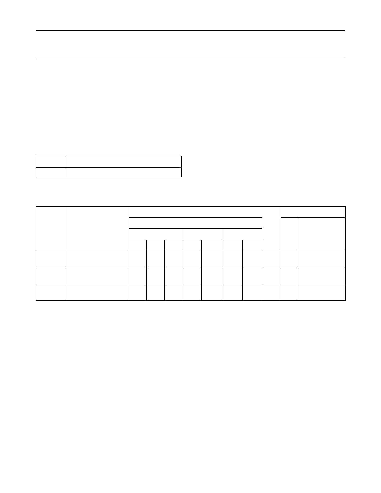
AC CHARACTERISTICS FOR 74HCT
GND = 0 V; tr=tf= 6 ns; CL= 50 pF
T
amb
(°C)
TEST CONDITIONS
74HCT
SYMBOL PARAMETER
+25 −40 to +85 −40 to +125
UNIT
V
(V)
CC
min. typ. max. min. max. min. max.
t
PHL
t
PHL
t
THL
/ t
/ t
/ t
propagation delay
PLH
In to ∑
E
propagation delay
PLH
In to ∑
O
output transition time 7 15 19 22 ns 4.5 Fig.6
TLH
21 42 53 63 ns 4.5 Fig.6
26 45 56 68 ns 4.5 Fig.6
WAVEFORMS
December 1990 6
Page 7
Philips Semiconductors Product specification
9-bit odd/even parity generator/checker 74HC/HCT280
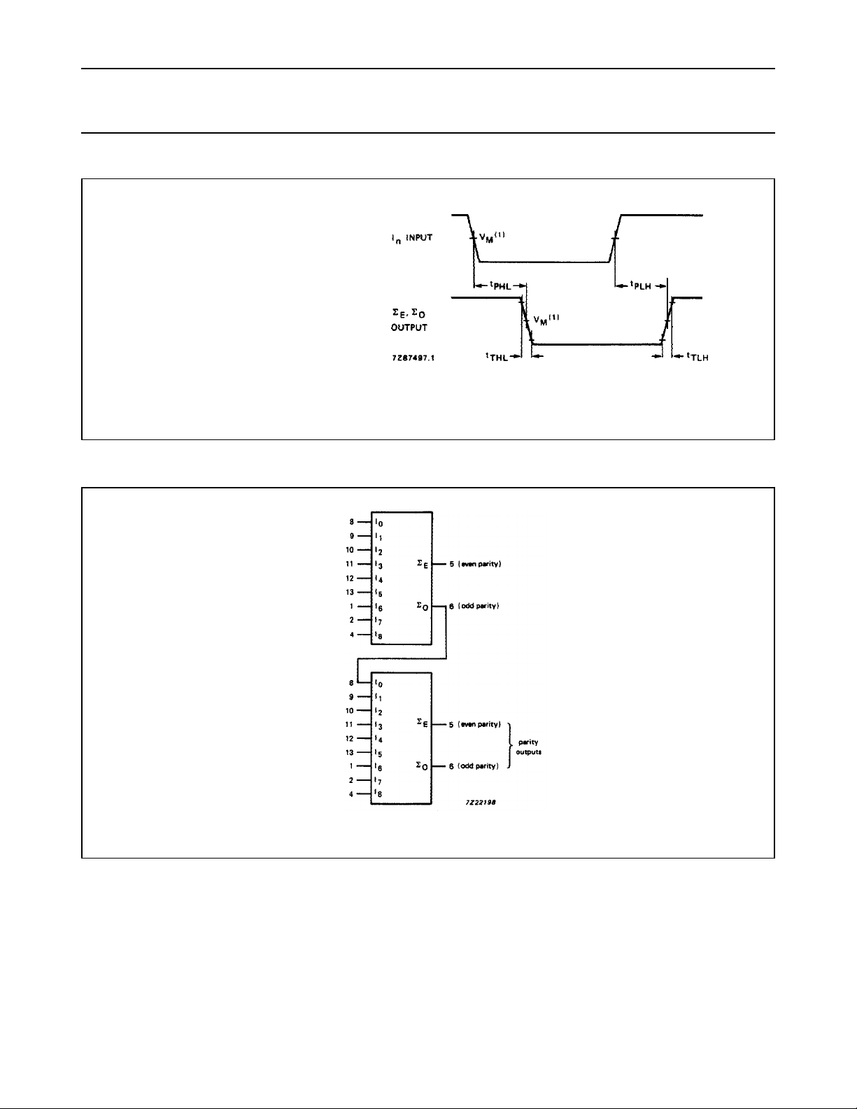
AC WAVEFORMS
(1) HC : VM= 50%; VI= GND to VCC.
= 1.3 V; VI= GND to 3 V.
HCT: V
M
Fig.6 Waveforms showing the data input (In) to parity outputs (∑E, ∑O) propagation delays and the output
transition time.
APPLICATION INFORMATION
For a single-chip 16-bit even/odd parity
generator/checker, see PC74HC/HCT7080.
Fig.7 Cascaded 17-bit odd/even parity generator/checker.
PACKAGE OUTLINES
“74HC/HCT/HCU/HCMOS Logic Package Outlines”
See
.
December 1990 7
 Loading...