

Page 1
INTEGRATED CIRCUITS
DATA SH EET
For a complete data sheet, please also download:
•The IC06 74HC/HCT/HCU/HCMOS Logic Family Specifications
•The IC06 74HC/HCT/HCU/HCMOS Logic Package Information
•The IC06 74HC/HCT/HCU/HCMOS Logic Package Outlines
74HC/HCT221
Dual non-retriggerable monostable
multivibrator with reset
Product specification
Supersedes data of April 1988
File under Integrated Circuits, IC06
December 1990
Page 2
Philips Semiconductors Product specification
Dual non-retriggerable monostable
multivibrator with reset
FEATURES
• Pulse width variance is typically less than ±5%
• Pin-out identical to “123”
• Overriding reset terminates output pulse
• nB inputs have hysteresis for improved noise immunity
• Output capability: standard (except for nR
EXT/CEXT
• ICC category: MSI
GENERAL DESCRIPTION
The 74HC/HCT221 are high-speed Si-gate CMOS devices
and are pin compatible with low power Schottky TTL
(LSTTL). They are specified in compliance with JEDEC
standard no. 7A.
The 74HC/HCT221 are dual non-retriggerable monostable
multivibrators. Each multivibrator features an active
LOW-going edge input (n
A) and an active HIGH-going
edge input (nB), either of which can be used as an enable
input.
Pulse triggering occurs at a particular voltage level and is
not directly related to the transition time of the input pulse.
Schmitt-trigger input circuitry for the nB inputs allow
)
74HC/HCT221
jitter-free triggering from inputs with slow transition rates,
providing the circuit with excellent noise immunity.
Once triggered, the outputs (nQ, nQ) are independent of
further transitions of nA and nB inputs and are a function
of the timing components. The output pulses can be
terminated by the overriding active LOW reset inputs
(nRD). Input pulses may be of any duration relative to the
output pulse.
Pulse width stability is achieved through internal
compensation and is virtually independent of VCC and
temperature. In most applications pulse stability will only
be limited by the accuracy of the external timing
components.
The output pulse width is defined by the following
relationship:
tW=C
EXTREXTIn2
tW= 0.7C
Pin assignments for the “221” are identical to those of the
“123” so that the “221” can be substituted for those
products in systems not using the retrigger by merely
changing the value of R
EXTREXT
and/or C
EXT
EXT
.
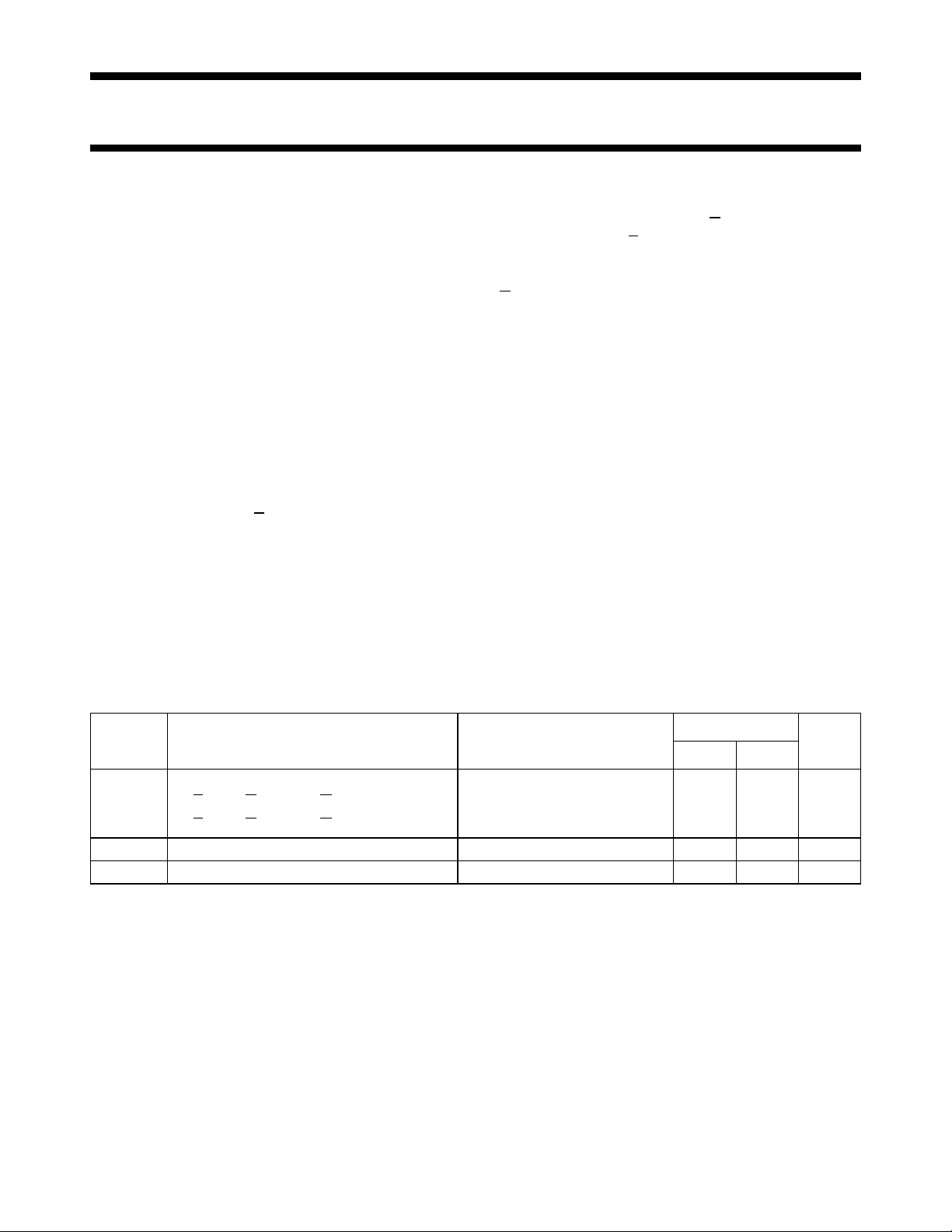
QUICK REFERENCE DATA
GND = 0 V; T
=25°C; tr=tf= 6 ns
amb
SYMBOL PARAMETER CONDITIONS
t
PHL
t
PLH
C
I
C
PD
propagation delay C
nA, nB, nRD to nQ, nQ 2932ns
nA, nB, nRD to nQ, nQ 3536ns
input capacitance 3.5 3.5 pF
power dissipation capacitance per package notes 1 and 2 90 96 pF
= 15 pF; VCC=5 V;
L
R
=5 kΩ; C
EXT
Notes
1. C
is used to determine the dynamic power dissipation (PD in µW):
PD
PD=CPD× V
2
× fi+∑(CL× V
CC
2
× fo) + 0.33 × C
CC
EXT
× V
CC
2
fi= input frequency in MHz; fo= output frequency in MHz
∑ (CL× V
C
EXT
2
× fo) = sum of outputs
CC
= timing capacitance in pF; CL= output load capacitance in pF
VCC= supply voltage in V; D = duty factor in %
2. For HC the condition is VI= GND to V
CC
For HCT the condition is VI= GND to VCC− 1.5 V
HC HCT
= 0 pF
EXT
× fo+ D × 28 × VCCwhere:
TYPICAL
UNIT
December 1990 2
Page 3
Philips Semiconductors Product specification
Dual non-retriggerable monostable
multivibrator with reset
ORDERING INFORMATION
See
“74HC/HCT/HCU/HCMOS Logic Package Information”
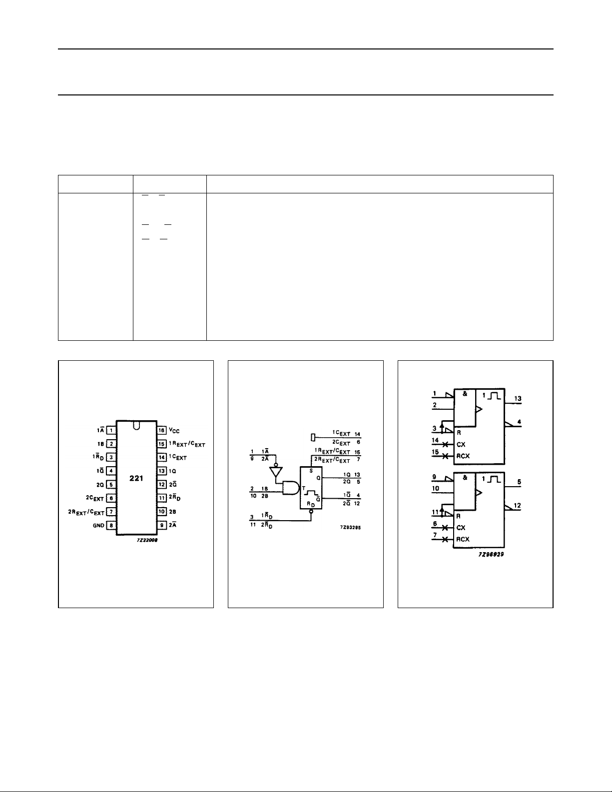
PIN DESCRIPTION
PIN NO. SYMBOL NAME AND FUNCTION
1, 9 1
2, 10 1B, 2B trigger inputs (positive-edge triggered)
3, 11 1
4, 12 1
72R
8 GND ground (0 V)
13, 5 1Q, 2Q outputs (active HIGH)
14, 6 1C
15 1R
16 V
A, 2A trigger inputs (negative-edge triggered)
RD, 2R
D
Q, 2Q outputs (active LOW)
EXT/CEXT
, 2C
EXT
EXT/CEXT
CC
EXT
direct reset inputs (active LOW)
external resistor/capacitor connection
external capacitor connection
external resistor/capacitor connection
positive supply voltage
.
74HC/HCT221
Fig.1 Pin configuration. Fig.2 Logic symbol. Fig.3 IEC logic symbol.
December 1990 3
Page 4
Philips Semiconductors Product specification
Dual non-retriggerable monostable
multivibrator with reset
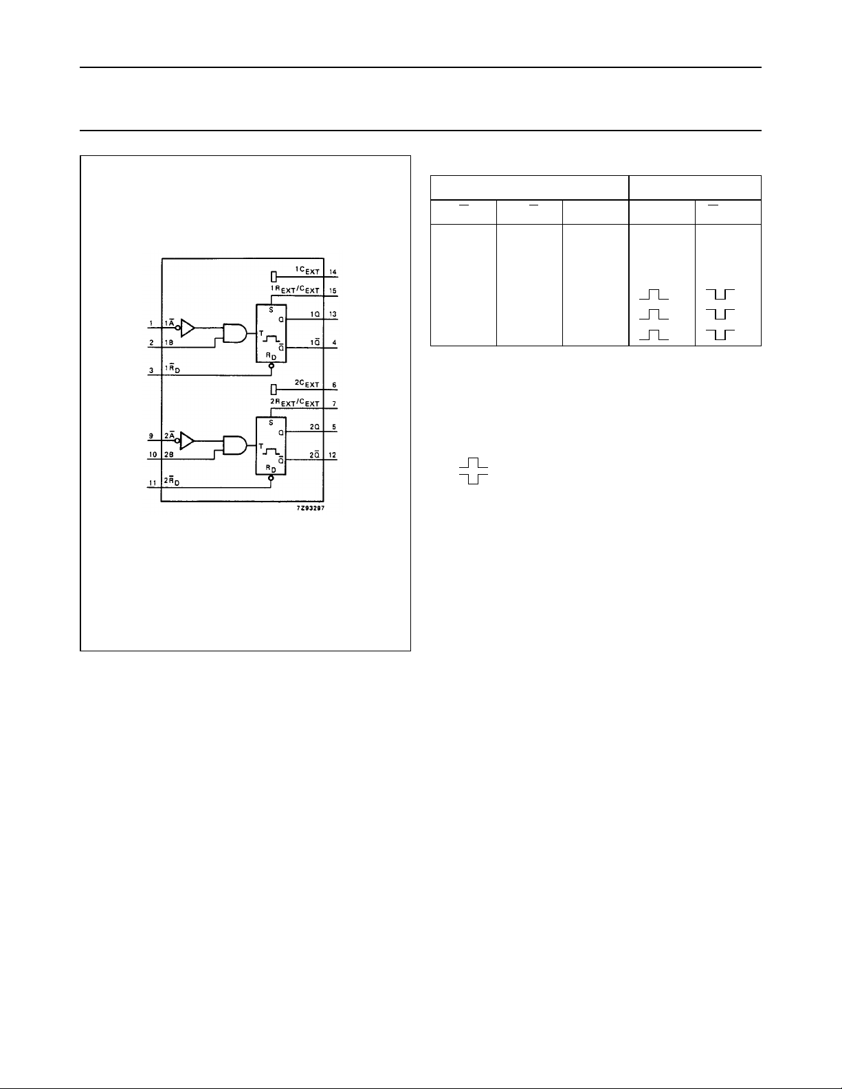
Fig.4 Functional diagram.
74HC/HCT221
FUNCTION TABLE
INPUTS OUTPUTS
nR
D
LXXLH
XHXL
XXLL
HL↑
H↓H
↑LH
Notes
1. H = HIGH voltage level
L = LOW voltage level
X = don’t care
↑ = LOW-to-HIGH level
↓ = HIGH-to-LOW level
2. If the monostable was triggered before this condition
was established the pulse will continue as
programmed.
3. For this combination the reset input must be LOW and
the following sequence must be used:
pin 1 (or 9) must be set HIGH or pin 2 (or 10) set LOW;
then pin 1 (or 9) must be LOW and pin 2 (or 10) set
HIGH. Now the reset input goes from LOW-to-HIGH
and the device will be triggered.
nAnBnQnQ
(2)
(2)
= one HIGH-level output pulse
= one LOW-level output pulse
H
H
(3) (3)
(2)
(2)
December 1990 4
Page 5
Philips Semiconductors Product specification
Dual non-retriggerable monostable
multivibrator with reset
74HC/HCT221
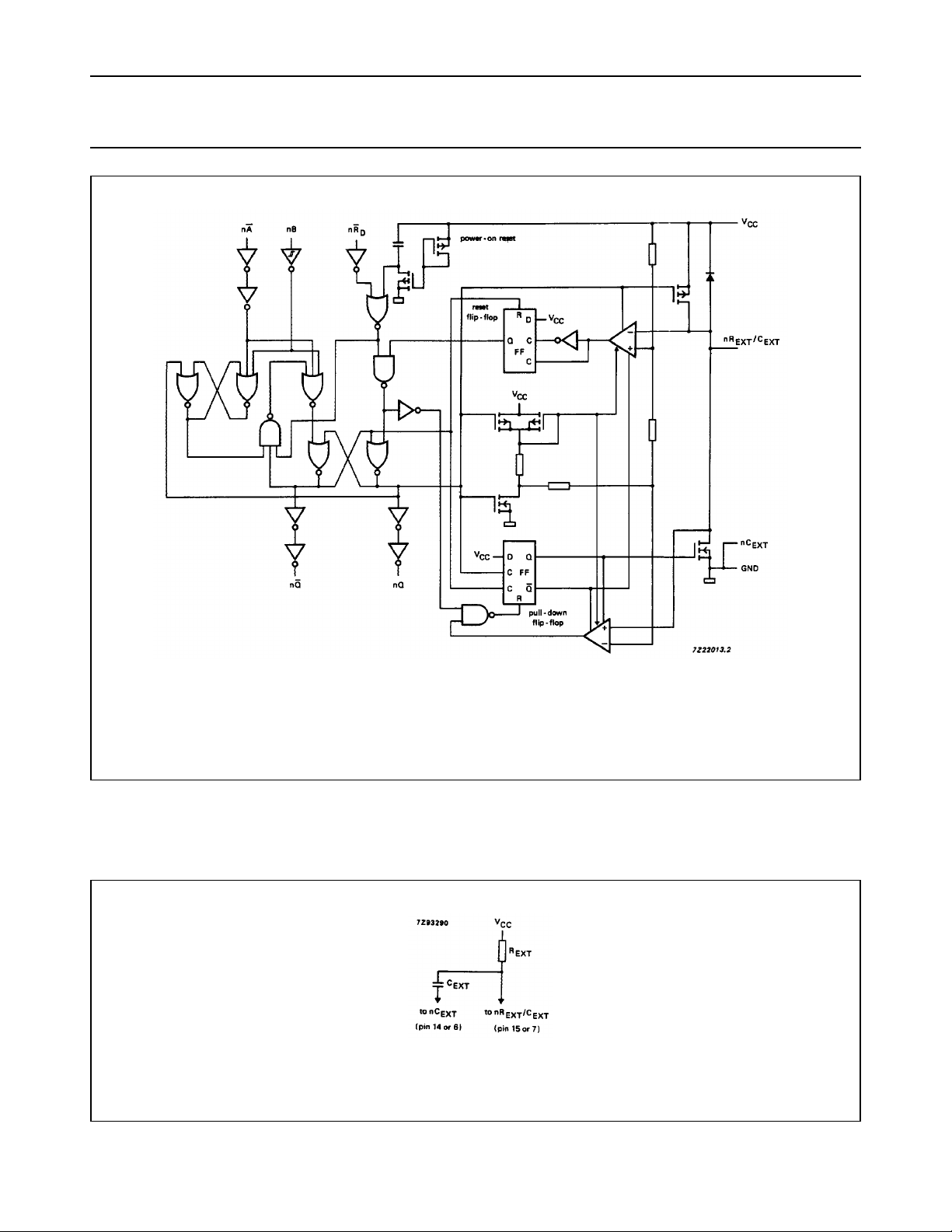
Fig.5 Logic diagram.
Note
It is recommended to ground pins 6 (2C
December 1990 5
) and 14 (1C
EXT
Fig.6 Timing component connections.
EXT
) externally to pin 8 (GND).
Page 6
Philips Semiconductors Product specification
Dual non-retriggerable monostable
multivibrator with reset
DC CHARACTERISTICS FOR 74HC
For the DC characteristics see
Output capability: standard (except for nR
ICC category: MSI
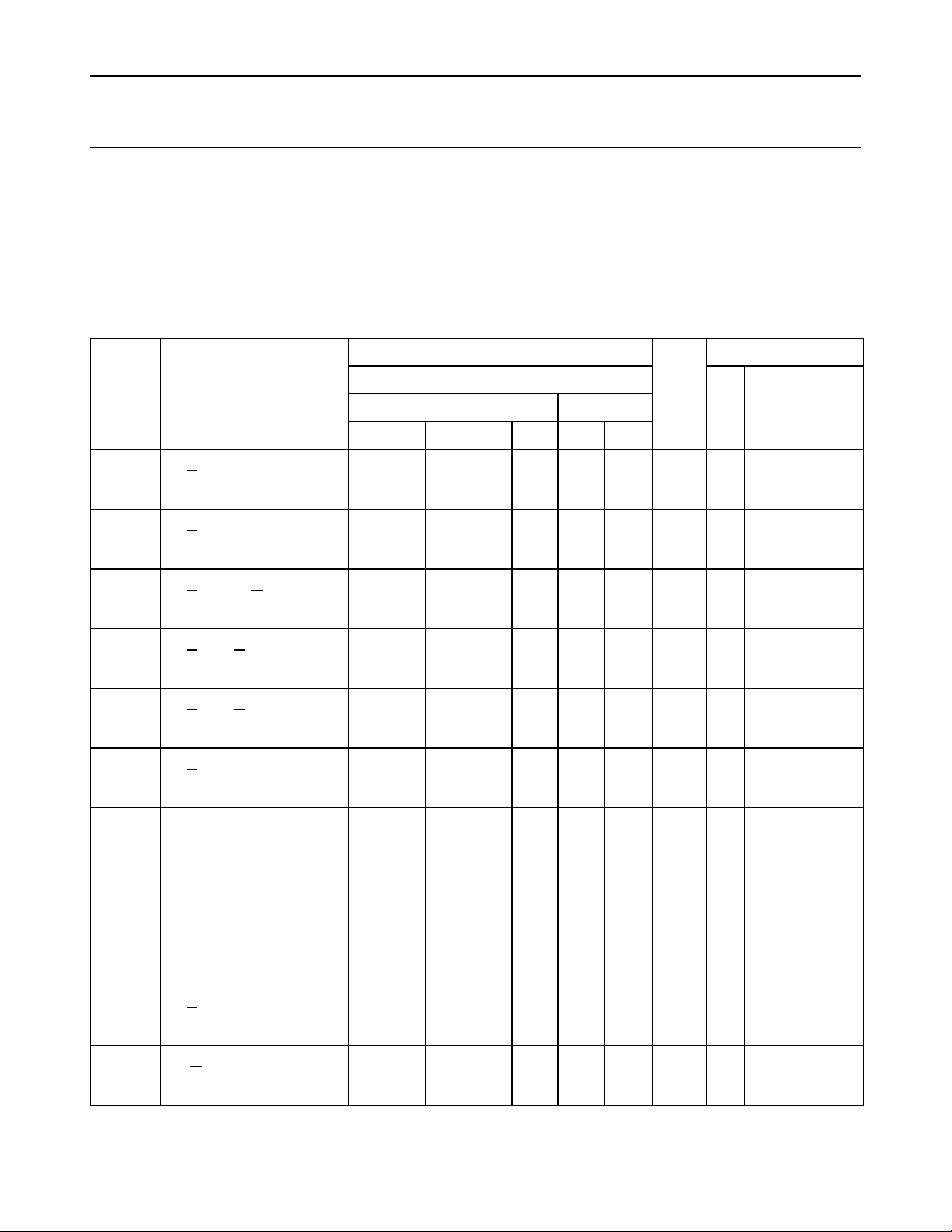
AC CHARACTERISTICS FOR 74HC
GND = 0 V; t
SYMBOL PARAMETER
t
PLH
= 6 ns; CL= 50 pF
r=tf
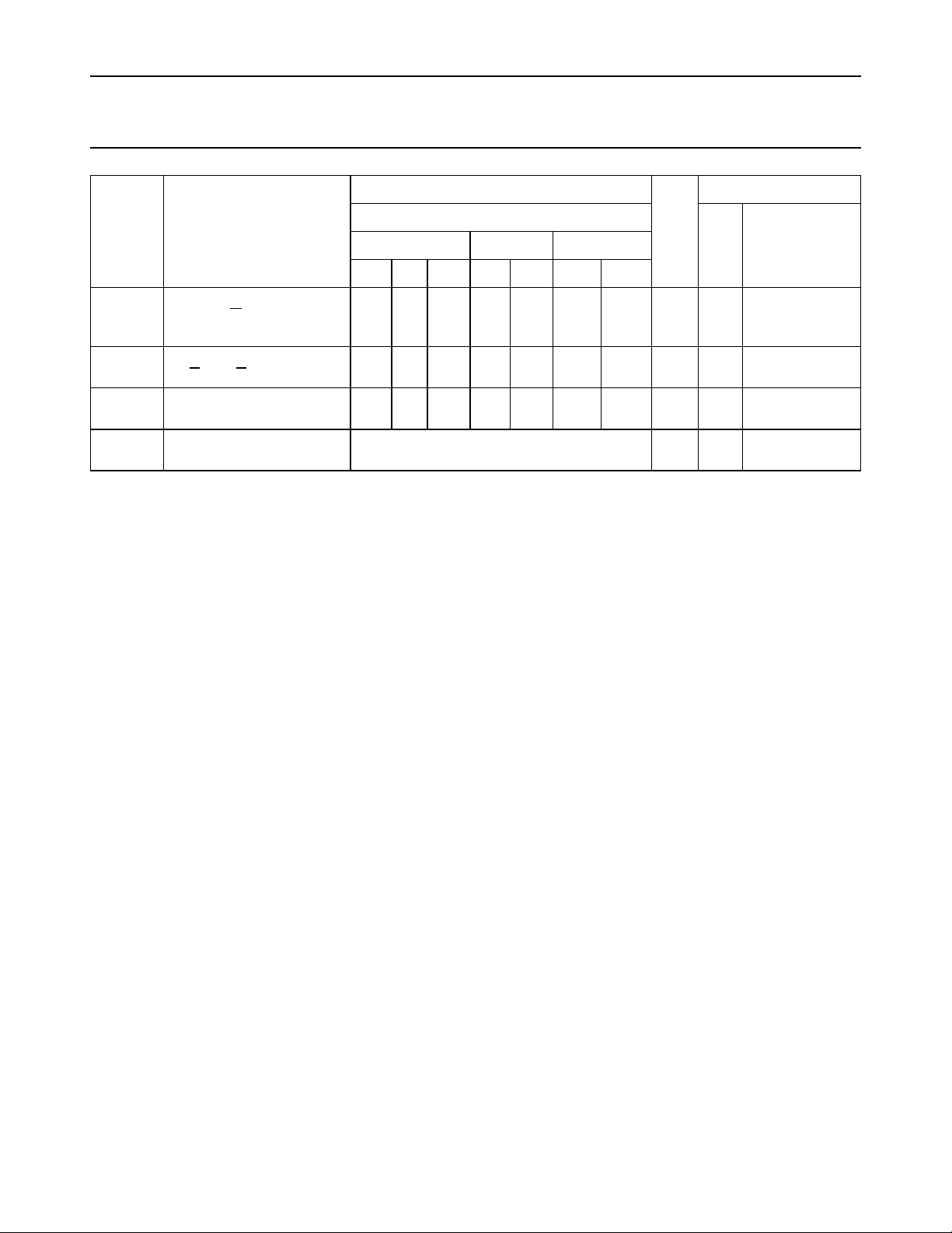
propagation delay (trigger)
nA, nB to nQ
t
PLH
propagation delay (trigger)
nRD to nQ
t
PHL
propagation delay (trigger)
nA, nB to nQ
t
PHL
propagation delay (trigger)
nRD to nQ
t
PLH
propagation delay (reset)
nRD to nQ
t
PLH
propagation delay (reset)
nRD to nQ
t
/
THL
t
TLH
t
W
output transition time 19
trigger pulse width
nA = LOW
t
W
trigger pulse width
nB = HIGH
t
W
trigger pulse width
nRD= LOW
t
W
output pulse width
nQ = LOW
nQ = HIGH
“74HC/HCT/HCU/HCMOS Logic Family Specifications”
EXT/CEXT
+25 −40 to +85 −40 to +125
min typ max. min max. min. max.
72
26
21
80
29
23
58
21
17
63
23
18
66
24
19
58
21
17
7
6
75
25
15
9
13
7
90
30
18
11
15
9
75
25
15
9
13
7
630 700 770 602 798 595 805 µs 5.0 C
74HC/HCT221
.
)
T
220
44
37
245
49
42
180
36
31
195
39
33
200
40
34
180
36
31
75
15
13
amb
74HC
95
19
16
115
23
20
95
19
16
(°C)
275
55
47
305
61
52
225
45
38
245
49
42
250
50
43
225
45
38
95
19
16
110
22
19
135
27
23
110
22
19
330
66
56
370
74
63
270
54
46
295
59
50
300
60
51
270
54
46
110
22
19
UNIT
ns 2.0
ns 2.0
ns 2.0
ns 2.0
ns 2.0
ns 2.0
ns 2.0
ns 2.0
ns 2.0
ns 2.0
TEST CONDITIONS
WAVEFORMS
V
CC
(V)
C
= 0 pF;
EXT
4.5
R
=5 kΩ;
EXT
6.0
Fig.10
C
= 0 pF;
EXT
4.5
R
=5 kΩ;
EXT
6.0
Fig.10
C
= 0 pF;
EXT
4.5
R
=5 kΩ;
EXT
6.0
Fig.10
C
= 0 pF;
EXT
4.5
R
=5 kΩ;
EXT
6,0
Fig.10
C
= 0 pF;
EXT
4.5
R
=5 kΩ;
EXT
6.0
Fig.11
C
= 0 pF;
EXT
4.5
R
=5 kΩ;
EXT
6.0
Fig.11
Fig.10
4.5
6.0
Fig.7
4.5
6.0
Fig.7
4.5
6.0
Fig.8
4.5
6.0
= 100 nF;
EXT
R
= 10 kΩ;
EXT
Fig.10
December 1990 6
Page 7
Philips Semiconductors Product specification
Dual non-retriggerable monostable
multivibrator with reset
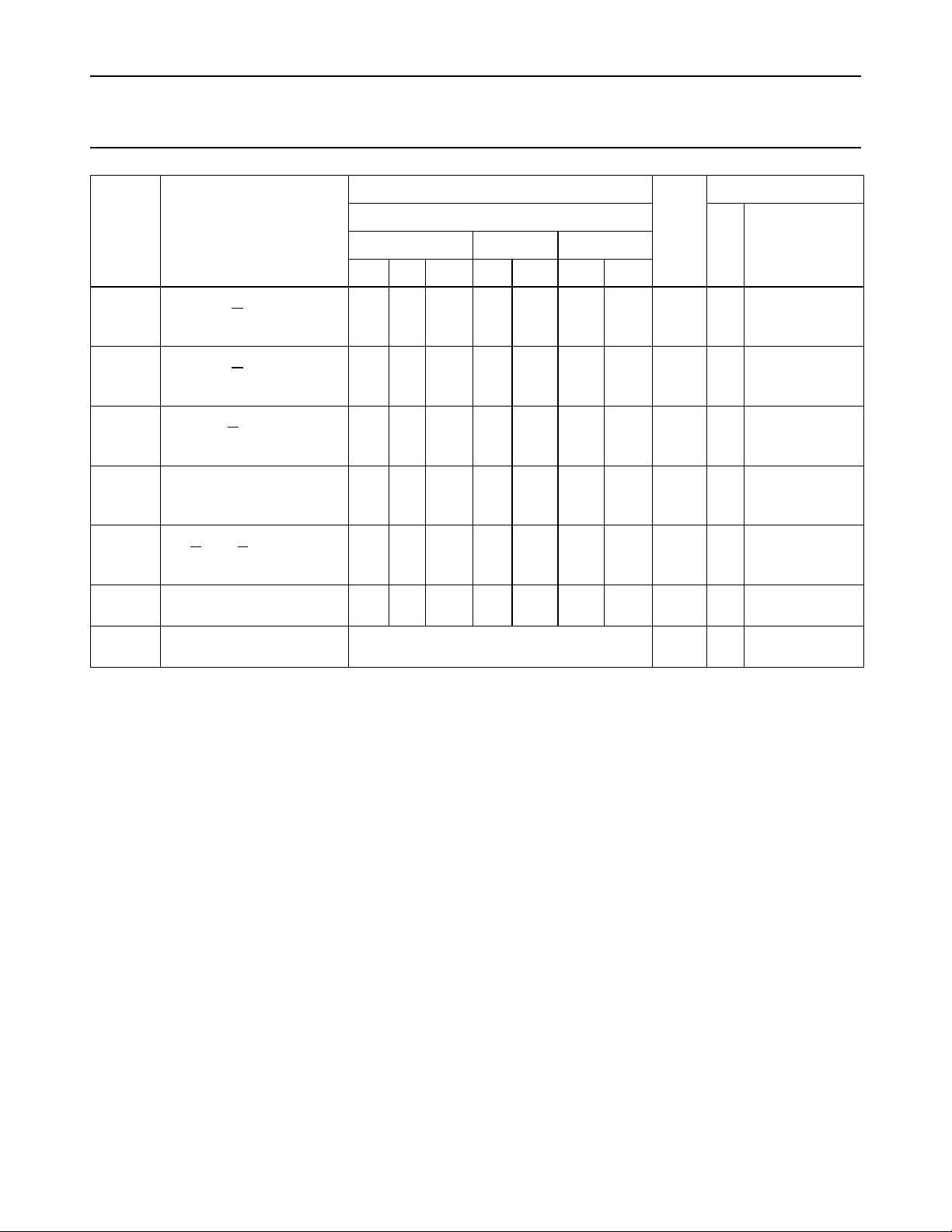
SYMBOL PARAMETER
t
W
output pulse width
nQ or nQ
t
W
output pulse width
nQ or nQ
t
W
output pulse width
nQ or nQ
t
W
pulse width match
between circuits
in the package
t
rem
removal time
nRD to nA
or nB
R
EXT
C
EXT
external timing resistor 10
external timing capacitor no limits pF 2.0
+25 −40 to +85 −40 to +125
min typ max. min max. min. max.
140 −− ns 2.0
1.5 −− µs 2.0
7 −− µs 2.0
± 2 −− % 4.5
100
30
20
11
17
9
2
T
1000
1000−−
amb
74HC
125
25
21
(°C)
150
30
26
−
−
74HC/HCT221
TEST CONDITIONS
UNIT
ns 2.0
kΩ 2.0
V
(V)
4.5
6.0
4.5
6.0
4.5
6.0
to
5.5
4.5
6.0
5.0
5.0
CC
WAVEFORMS
C
= 28 nF;
EXT
R
=2 kΩ;
EXT
Fig.10
C
= 1 nF;
EXT
R
=2 kΩ;
EXT
Fig.10
C
= 1 nF;
EXT
R
= 10 kΩ;
EXT
Fig.10
C
= 1000 pF;
EXT
R
= 10 kΩ
EXT
Fig.9
Fig.12
Fig.13
Fig.12
Fig.13
December 1990 7
Page 8

Philips Semiconductors Product specification
Dual non-retriggerable monostable
74HC/HCT221
multivibrator with reset
DC CHARACTERISTICS FOR 74HCT
For the DC characteristics see
Output capability: standard (except for nR
ICC category: MSI
Note to HCT types
The value of additional quiescent supply current (∆I
To determine ∆ICC per input, multiply this value by the unit load coefficient shown in the table below.
INPUT UNIT LOAD COEFFICIENT
nB 0.30
n
A 0.50
n
R
D
0.50
“74HC/HCT/HCU/HCMOS Logic Family Specifications”
EXT/CEXT
)
) for a unit load of 1 is given in the family specifications.
CC
.
December 1990 8
Page 9
Philips Semiconductors Product specification
Dual non-retriggerable monostable
multivibrator with reset
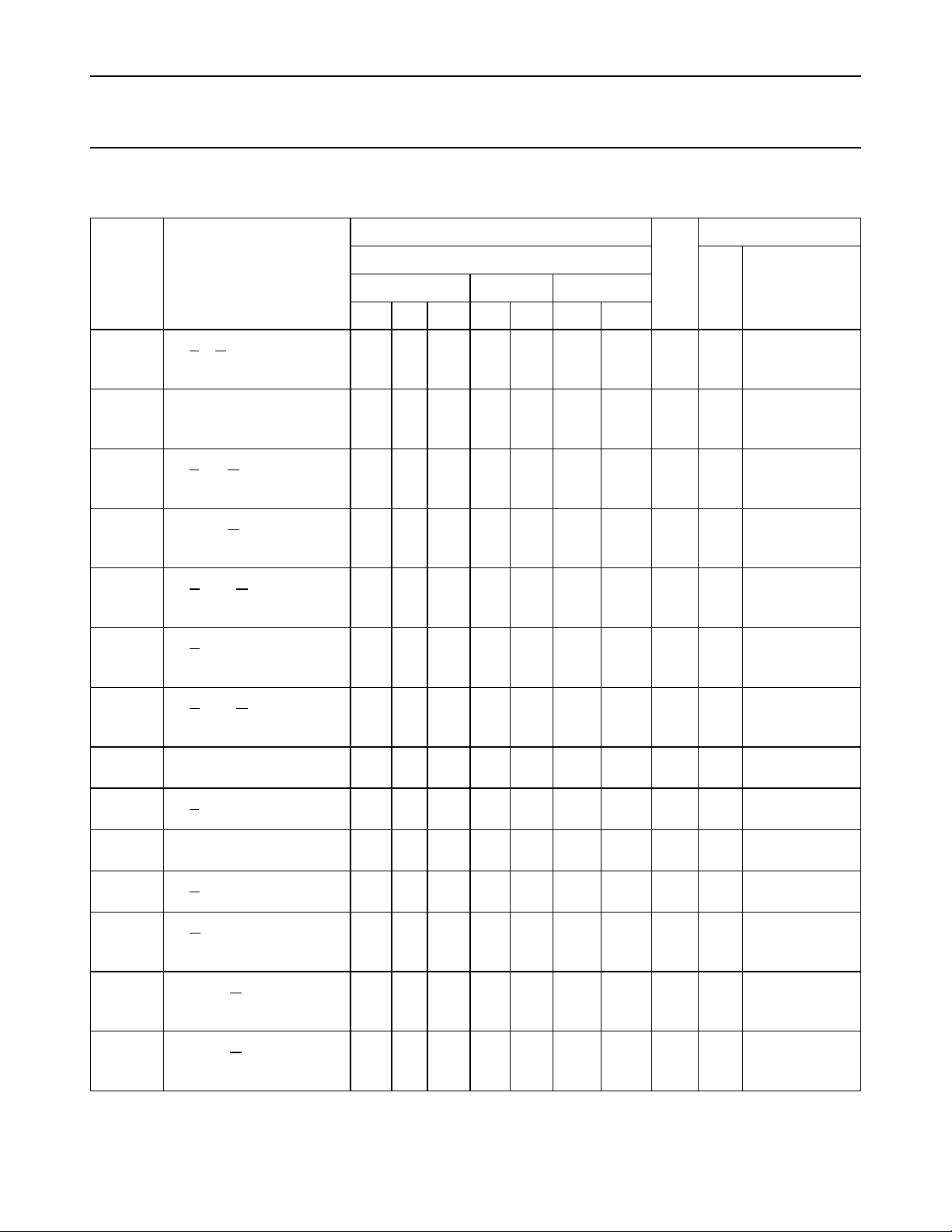
AC CHARACTERISTICS FOR 74HCT
GND = 0 V; t
SYMBOL PARAMETER
t
PLH
t
PLH
t
PHL
t
PHL
t
PHL
t
PHL
t
PLH
/ t
t
THL
TLH
= 6 ns; CL= 50 pF
r=tf
+25 −40 to +85 −40 to +125
min typ max min max. min. max.
propagation delay (trigger)
30 50 63 75 ns 4.5 C
nA, nRD to nQ
propagation delay (trigger)
24 42 53 63 ns 4.5 C
nB to nQ
propagation delay (trigger)
26 44 55 66 ns 4.5 C
nA to nQ
propagation delay (trigger)
21 35 44 53 ns 4.5 C
nB to nQ
propagation delay (trigger)
26 43 54 65 ns 4.5 C
nRD to nQ
propagation delay (reset)
26 43 54 65 ns 4.5 C
nRD to nQ
propagation delay (reset)
31 51 64 77 ns 4.5 C
nRD to nQ
output transition time 7 15 19 22 ns 4.5 Fig.10
T
amb
74HCT
(°C)
74HC/HCT221
TEST CONDITIONS
UNIT
V
(V)
CC
R
Fig.10
R
Fig.10
R
Fig.10
R
Fig.10
R
Fig.10
R
Fig.11
R
Fig.11
WAVEFORMS
= 0 pF;
EXT
=5 kΩ;
EXT
= 0 pF;
EXT
=5 kΩ;
EXT
= 0 pF;
EXT
=5 kΩ;
EXT
= 0 pF;
EXT
=5 kΩ;
EXT
= 0 pF;
EXT
=5 kΩ;
EXT
= 0 pF;
EXT
=5 kΩ;
EXT
= 0 pF;
EXT
=5 kΩ;
EXT
t
W
trigger pulse width
20 13 25 30 ns 4.5 Fig.10
nA = LOW
t
W
trigger pulse width
20 13 25 30 ns 4.5 Fig.10
nB = HIGH
t
W
pulse width
22 13 28 33 ns 4.5 Fig.8
nRD= LOW
t
W
output pulse width
630 700 770 602 798 595 805 µs 5.0 C
nQ = LOW
nQ = HIGH
t
W
trigger pulse width
140 −− ns 4.5 C
nQ or nQ
t
W
trigger pulse width
1.5 −− µs 4.5 C
nQ or nQ
December 1990 9
EXT
R
EXT
Fig.10
EXT
R
EXT
Fig.10
EXT
R
EXT
Fig.10
= 100 nF;
= 10 kΩ;
= 28 pF;
=2 kΩ;
= 1 nF;
= 2 kΩ;
Page 10
Philips Semiconductors Product specification
Dual non-retriggerable monostable
multivibrator with reset
SYMBOL PARAMETER
t
W
trigger pulse width
nQ or nQ
t
rem
removal time
nRD to nA or nB
R
EXT
C
EXT
external timing resistor 2 1000 −− kΩ5.0 Fig.13
external timing capacitor no limits pF 5.0 Fig.13
+25 −40 to +85 −40 to +125
min typ max min max. min. max.
7 −− µs 4.5 C
20 12 25 30 ns 4.5 Fig.9
T
amb
74HCT
(°C)
74HC/HCT221
TEST CONDITIONS
UNIT
V
(V)
CC
R
Fig.10
WAVEFORMS
= 1 nF;
EXT
= 10 kΩ;
EXT
December 1990 10
Page 11
Philips Semiconductors Product specification
Dual non-retriggerable monostable
multivibrator with reset
AC WAVEFORMS
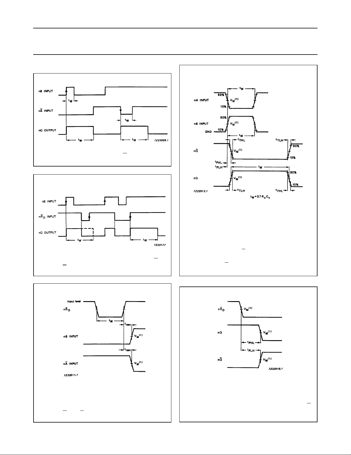
Fig.7 Output pulse control; nRD= HIGH.
74HC/HCT221
Fig.8 Output pulse control using reset input nRD;
nA = LOW.
(1) HC : VM=VM= 50%; VI= GND to VCC.
HCT : V
= 1.3 V; VI= GND to 3 V.
M=VM
(1) HC : VM=VM= 50%; VI= GND to VCC.
HCT : V
= 1.3 V; VI= GND to 3 V.
M=VM
Fig.10 Waveforms showing the triggering of One
Shot by input nA or input nB for one period
(tW) and minimum pulse widths of the trigger
inputs nA and nB.
(1) HC : VM=VM= 50%; VI= GND to VCC.
HCT : V
= 1.3 V; VI= GND to 3 V.
M=VM
Fig.9 Waveforms showing the removal times;
nRD to nA or nB.
December 1990 11
Fig.11 Waveforms showing the reset to nQ and nQ
output propagation delays.
Page 12
Philips Semiconductors Product specification
Dual non-retriggerable monostable
multivibrator with reset
74HC/HCT221
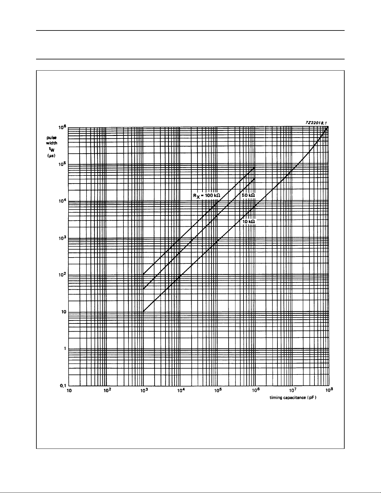
Fig.12 HC typical output pulse width as a function of timing capacitance (VCC = 2 V).
December 1990 12
Page 13
Philips Semiconductors Product specification
Dual non-retriggerable monostable
multivibrator with reset
74HC/HCT221
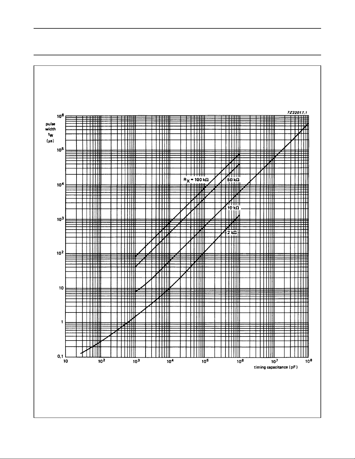
Fig.13 HC/HCT typical output pulse width as a function of timing capacitance (VCC= 4.5 V).
December 1990 13
Page 14
Philips Semiconductors Product specification
Dual non-retriggerable monostable
multivibrator with reset
74HC/HCT221
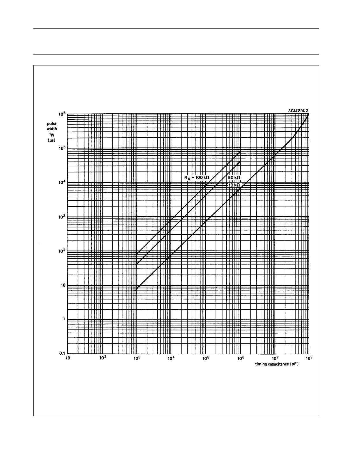
Fig.14 HC typical output pulse width as a function of timing capacitance (VCC= 6 V).
December 1990 14
Page 15
Philips Semiconductors Product specification
Dual non-retriggerable monostable
multivibrator with reset
74HC/HCT221
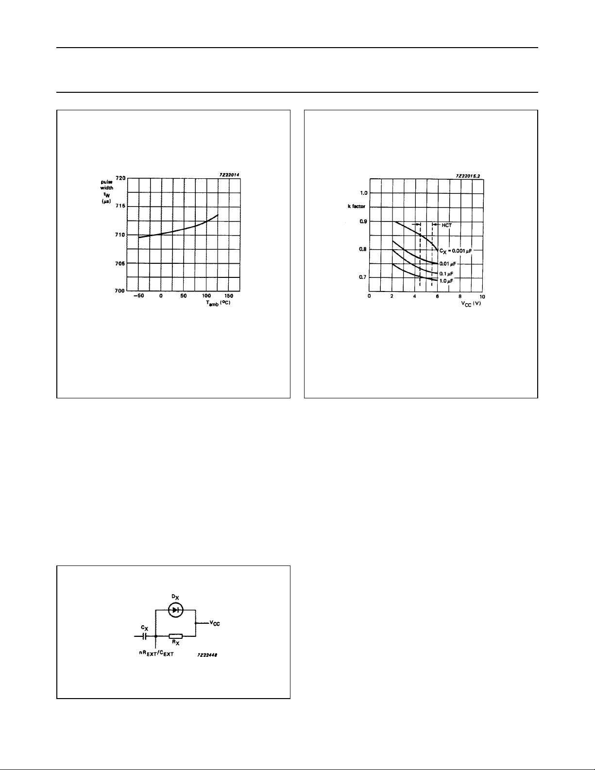
Fig.15 Typical output pulse width as a function of
temperature; CX= 0.1 µF; RX=10KΩ;
VCC=5V.
Power-down consideration
A large capacitor (CX) may cause problems when
powering-down the monostable due to the energy stored
in this capacitor. When a system containing this device is
powered-down or a rapid decrease of VCC to zero occurs,
the monostable may substain damage, due to the
capacitor discharging through the input protection diodes.
To avoid this possibility, use a damping diode (DX)
preferably a germanium or Schottky type diode able to
withstand large current surges and connect as shown in
Fig.17.
Fig.16 k factor as a function of supply voltage;
RX=10KΩ;T
PACKAGE OUTLINES
See
“74HC/HCT/HCU/HCMOS Logic Package Outlines”
amb
=25°C.
.
Fig.17 Power-down protection circuit.
December 1990 15
 Loading...