

Page 1
INTEGRATED CIRCUITS
DATA SH EET
For a complete data sheet, please also download:
•The IC06 74HC/HCT/HCU/HCMOS Logic Family Specifications
•The IC06 74HC/HCT/HCU/HCMOS Logic Package Information
•The IC06 74HC/HCT/HCU/HCMOS Logic Package Outlines
74HC/HCT192
Presettable synchronous BCD
decade up/down counter
Product specification
File under Integrated Circuits, IC06
December 1990
Page 2

Philips Semiconductors Product specification
Presettable synchronous BCD decade
up/down counter
FEATURES
• Synchronous reversible counting
• Asynchronous parallel load
• Asynchronous reset
• Expandable without external logic
• Output capability: standard
• ICC category: MSI
GENERAL DESCRIPTION
The 74HC/HCT192 are high-speed Si-gate CMOS devices
and are pin compatible with low power Schottky TTL
(LSTTL). They are specified in compliance with JEDEC
standard no. 7A.
The 74HC/HCT192 are synchronous BCD up/down
counters. Separate up/down clocks, CP
respectively, simplify operation. The outputs change state
synchronously with the LOW-to-HIGH transition of either
clock input. If the CPU clock is pulsed while CPD is held
HIGH, the device will count up. If the CPD clock is pulsed
while CPU is held HIGH, the device will count down. Only
one clock input can be held HIGH at any time, or
erroneous operation will result. The device can be cleared
at any time by the asynchronous master reset input (MR);
it may also be loaded in parallel by activating the
asynchronous parallel load input (PL).
The “192” contains four master-slave JK flip-flops with the
necessary steering logic to provide the asynchronous
reset, load, and synchronous count up and count down
functions.
Each flip-flop contains JK feedback from slave to master,
such that a LOW-to-HIGH transition on the CPD input will
decrease the count by one, while a similar transition on the
CPU input will advance the count by one.
and CP
U
D
74HC/HCT192
One clock should be held HIGH while counting with the
other, otherwise the circuit will either count by two’s or not
at all, depending on the state of the first flip-flop, which
cannot toggle as long as either clock input is LOW.
Applications requiring reversible operation must make the
reversing decision while the activating clock is HIGH to
avoid erroneous counts.
The terminal count up (TCU) and terminal count down
(TCD) outputs are normally HIGH. When the circuit has
reached the maximum count state of 9, the next
HIGH-to-LOW transition of CPU will causeTCU to go LOW.
TCU will stay LOW until CPU goes HIGH again, duplicating
the count up clock.
Likewise, the TCD output will go LOW when the circuit is in
the zero state and the CPD goes LOW. The terminal count
outputs can be used as the clock input signals to the next
higher order circuit in a multistage counter, since they
duplicate the clock waveforms. Multistage counters will not
be fully synchronous, since there is a slight delay time
difference added for each stage that is added.
The counter may be preset by the asynchronous parallel
load capability of the circuit. Information present on the
parallel data inputs (D0 to D3) is loaded into the counter
and appears on the outputs (Q0 to Q3) regardless of the
conditions of the clock inputs when the parallel load (PL)
input is LOW. A HIGH level on the master reset (MR) input
will disable the parallel load gates, override both clock
inputs and set all outputs (Q0 to Q3) LOW. If one of the
clock inputs is LOW during and after a reset or load
operation, the next LOW-to-HIGH transition of that clock
will be interpreted as a legitimate signal and will be
counted.
December 1990 2
Page 3
Philips Semiconductors Product specification
Presettable synchronous BCD decade
up/down counter
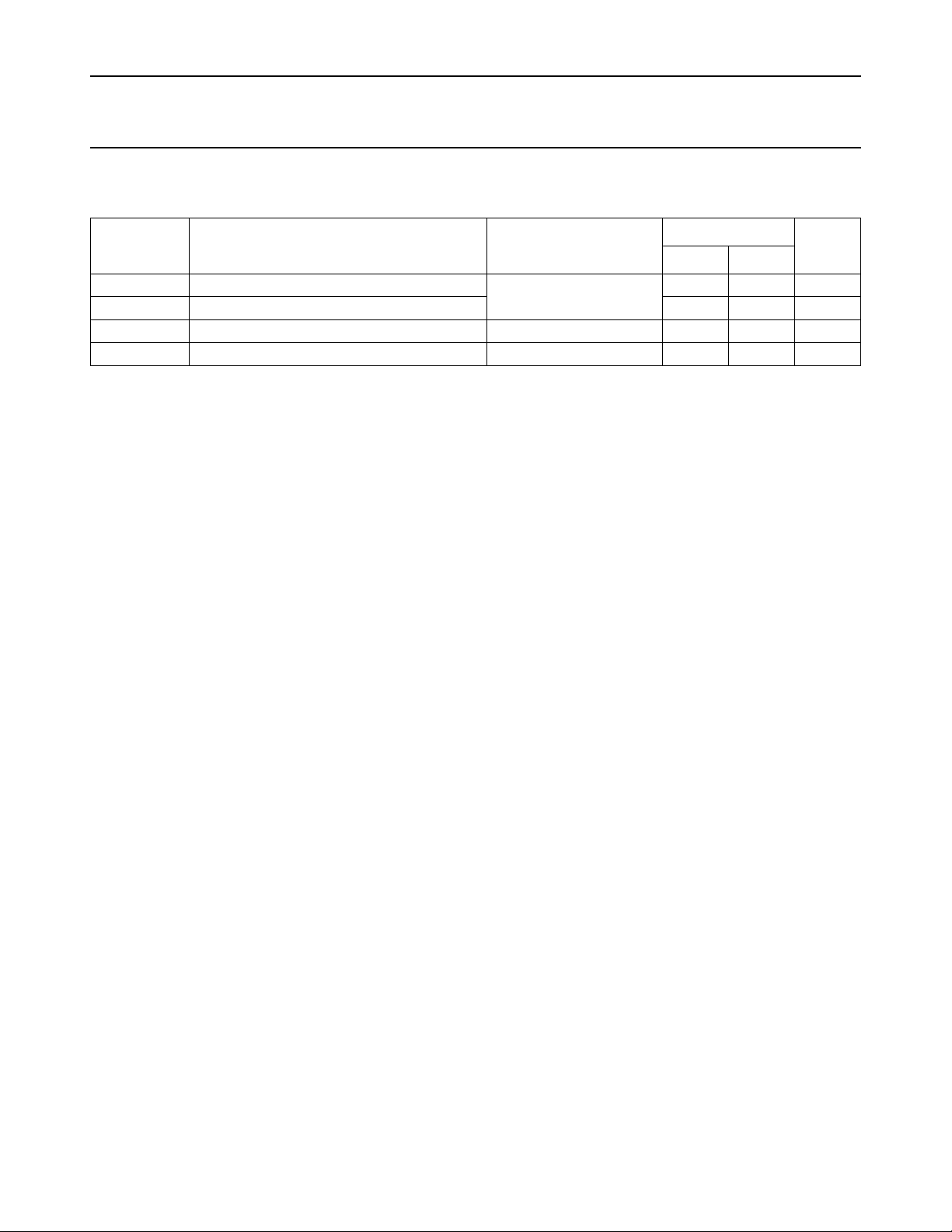
QUICK REFERENCE DATA
GND = 0 V; T
SYMBOL PARAMETER CONDITIONS
t
/ t
PHL
PLH
f
max
C
I
C
PD
Notes
1. C
is used to determine the dynamic power dissipation (PD in µW):
PD
PD=CPD× V
fi= input frequency in MHz
fo= output frequency in MHz
∑ (CL× V
CL= output load capacitance in pF
VCC= supply voltage in V
2. For HC the condition is VI= GND to V
For HCT the condition is VI= GND to VCC−1.5 V
=25°C; tr=tf= 6 ns
amb
propagation delay CPD, CPU to Q
maximum clock frequency 40 45 MHz
n
CL= 15 pF; VCC=5V
input capacitance 3.5 3.5 pF
power dissipation capacitance per package notes 1 and 2 24 28 pF
2
× fi+∑ (CL× V
CC
2
× fo) = sum of outputs
CC
2
× fo) where:
CC
CC
74HC/HCT192
TYPICAL
UNIT
HC HCT
20 20 ns
ORDERING INFORMATION
“74HC/HCT/HCU/HCMOS Logic Package Information”
See
.
December 1990 3
Page 4
Philips Semiconductors Product specification
Presettable synchronous BCD decade
up/down counter
PIN DESCRIPTION
PIN NO. SYMBOL NAME AND FUNCTION
3, 2, 6, 7 Q
4CP
5CP
8 GND ground (0 V)
11
12
13
14 MR asynchronous master reset input (active HIGH)
15, 1, 10, 9 D
16 V
Note
1. LOW-to-HIGH, edge triggered
to Q
0
3
D
U
flip-flop outputs
count down clock input
count up clock input
(1)
(1)
PL asynchronous parallel load input (active LOW)
TC
TC
U
D
to D
0
CC
3
terminal count up (carry) output (active LOW)
terminal count down (borrow) output (active LOW)
data inputs
positive supply voltage
74HC/HCT192
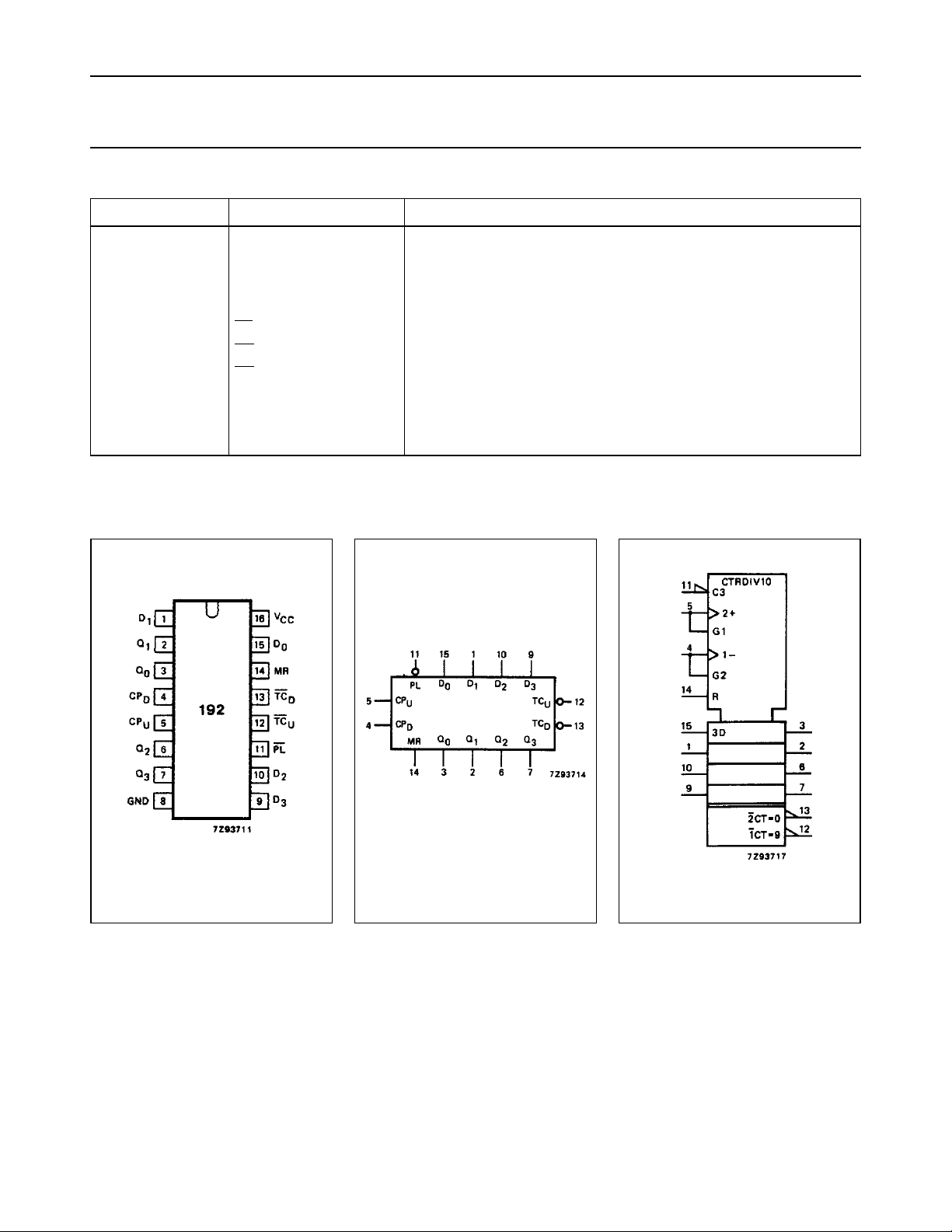
Fig.1 Pin configuration. Fig.2 Logic symbol. Fig.3 IEC logic symbol.
December 1990 4
Page 5
Philips Semiconductors Product specification
Presettable synchronous BCD decade
74HC/HCT192
up/down counter
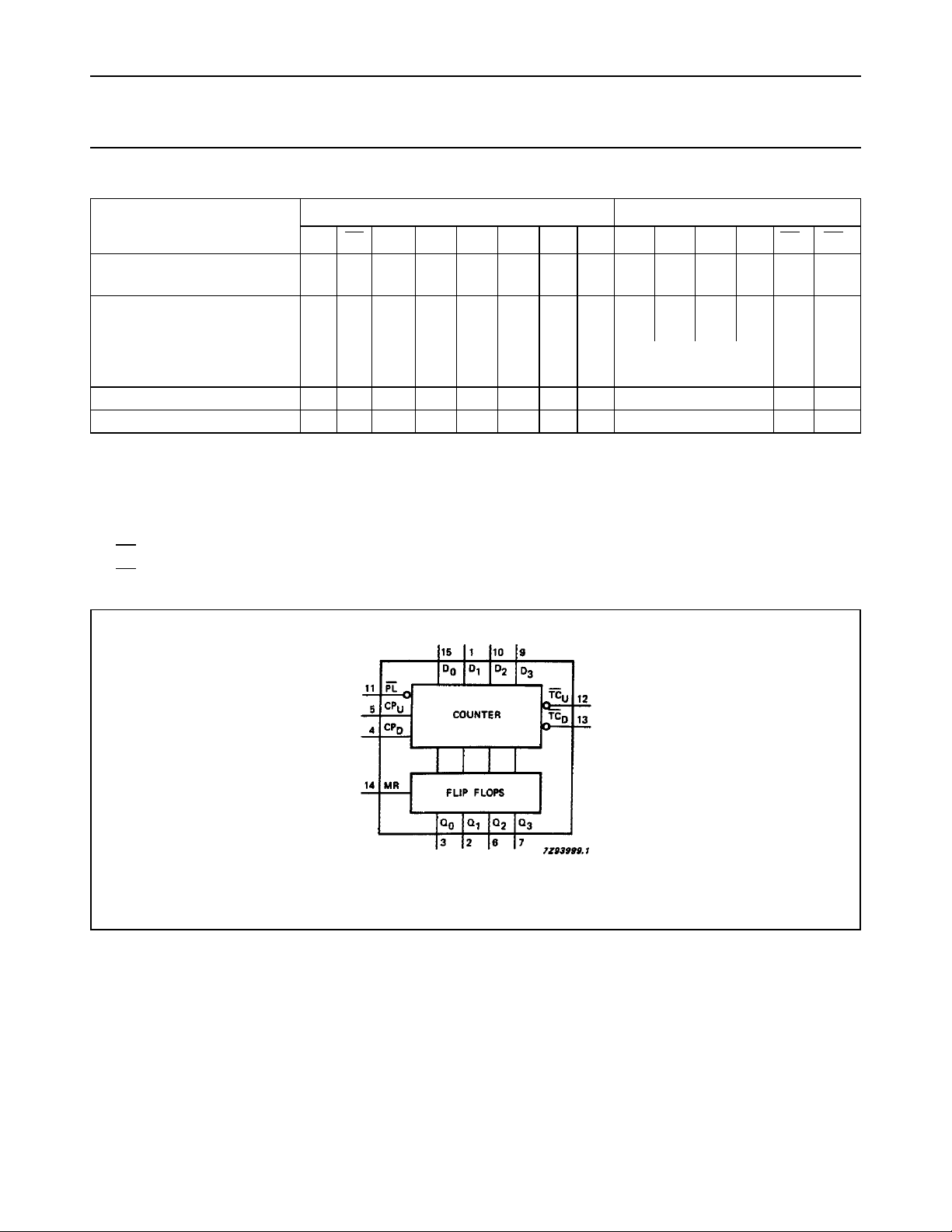
FUNCTION TABLE
OPERATING MODE
reset (clear)
parallel load
count up L H ↑ H X X X X count up H
count down L H H ↑ X X X X count down H H
Notes
1. H = HIGH voltage level
L = LOW voltage level
X = don’t care
↑ = LOW-to-HIGH clock transition
TCU=CPU at terminal count up (HLLH)
2.
3. TCD=CPD at terminal count down (LLLL)
PL CPUCPDD
MR
HHXXX
X
LLXLLLLLLLLLHL
LLXHLLLLLLLLHH
LLL X H X XH Q
LLH X H X XH Q
INPUTS OUTPUTS
D1D2D3Q0Q1Q2Q3TCUTC
0
L
HXXXX
XXXXL
L
L
L
L
L
n=Dn
n=Dn
LLHHL
LH
HH
(2)
D
H
H
(3)
Fig.4 Functional diagram.
December 1990 5
Page 6
Philips Semiconductors Product specification
Presettable synchronous BCD decade
up/down counter
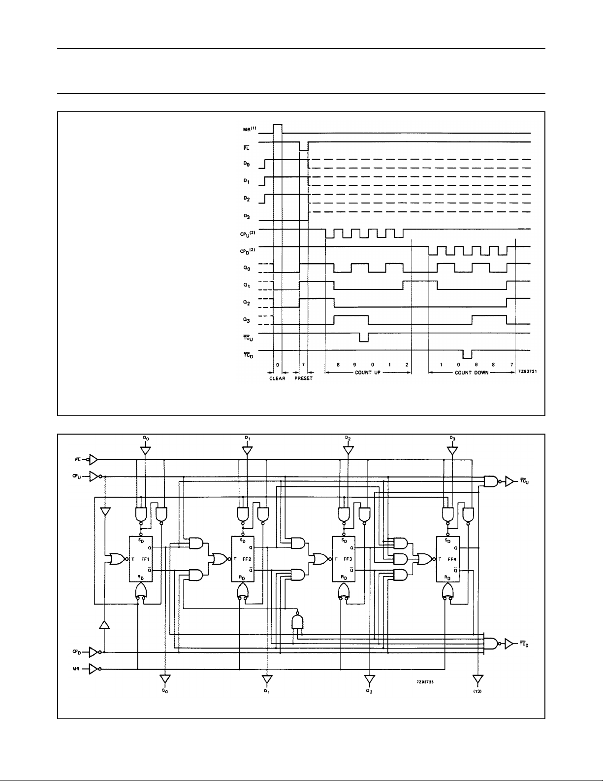
(1) Clear overrides load, data and count inputs.
(2) When counting up the count down clock input
Sequence
Clear (reset outputs to zero);
load (preset) to BCD seven;
count up to eight, nine,
count down to one, zero,
) must be HIGH, when counting down the
(CP
D
count up clock input (CP
terminal count up, zero,
one and two;
terminal count down, nine,
eight, and seven.
) must be HIGH.
U
74HC/HCT192
Fig.5 Typical clear, load and count sequence.
Fig.6 Logic diagram.
December 1990 6
Page 7
Philips Semiconductors Product specification
Presettable synchronous BCD decade
up/down counter
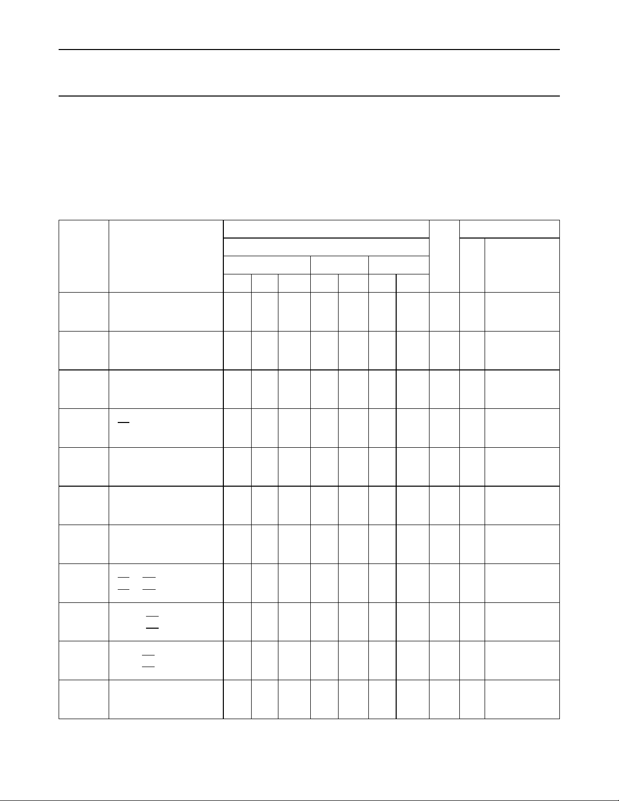
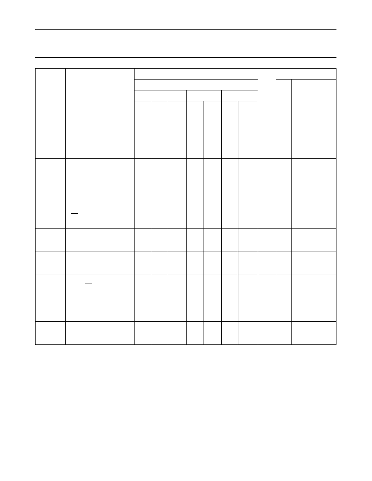
DC CHARACTERISTICS FOR 74HC
For the DC characteristics see
Output capability: standard
ICC category: MSI
AC CHARACTERISTICS FOR 74HC
GND = 0 V; t
SYMBOL PARAMETER
/ t
t
PHL
PLH
= 6 ns; CL=50pF
r=tf
propagation delay
CPU, CPD to Q
t
PHL
/ t
propagation delay
PLH
CPU to TC
t
PHL
/ t
propagation delay
PLH
CPD to TC
t
PHL
t
PHL
t
PHL
t
PLH
t
PHL
t
PHL
t
PHL
/ t
/ t
/ t
/ t
propagation delay
PLH
PL to Q
propagation delay
MR to Q
propagation delay
Dn to Q
propagation delay
Dn to Q
propagation delay
PLH
PL to TC
PL to TC
propagation delay
PLH
MR to TC
MR to TC
propagation delay
PLH
n
n
n
n
U,
D
U,
D
Dn to TCU,
t
THL
Dn to TC
/ t
output transition time 19
TLH
D
“74HC/HCT/HCU/HCMOS Logic Family Specifications”
+25 −40 to +85 −40 to +125
min. typ. max. min. max. min. max.
66
215
24
19
33
12
10
39
14
11
69
25
20
63
23
18
91
33
26
80
29
23
102
37
30
96
35
28
83
30
24
43
37
125
25
21
125
25
21
215
43
37
200
40
34
275
55
47
240
48
41
315
63
54
285
57
48
290
58
49
n
U
D
75
7
15
6
13
T
amb
74HC
(°C)
270
54
46
155
31
26
155
31
26
270
54
46
250
50
43
345
69
59
300
60
51
395
79
67
355
71
60
365
73
62
95
19
16
325
65
55
190
38
32
190
38
32
325
65
55
300
60
51
415
83
71
360
72
61
475
95
81
430
86
73
435
87
74
110
22
19
.
UNIT
ns 2.0
ns 2.0
ns 2.0
ns 2.0
ns 2.0
ns 2.0
ns 2.0
ns 2.0
ns 2.0
ns 2.0
ns 2.0
74HC/HCT192
TEST CONDITIONS
WAVEFORMS
V
CC
(V)
Fig.7
4.5
6.0
Fig.8
4.5
6.0
Fig.8
4.5
6.0
Fig.9
4.5
6.0
Fig.10
4.5
6.0
Fig.9
4.5
6.0
Fig.9
4.5
6.0
Fig.12
4.5
6.0
Fig.12
4.5
6.0
Fig.12
4.5
6.0
Fig.10
4.5
6.0
December 1990 7
Page 8
Philips Semiconductors Product specification
Presettable synchronous BCD decade
up/down counter
SYMBOL PARAMETER
t
W
up clock pulse width
HIGH or LOW
t
W
down clock pulse width
HIGH or LOW
t
W
master reset pulse width
HIGH
t
W
parallel load pulse width
LOW
t
t
t
rem
rem
su
removal time
PL to CPU, CP
removal time
MR to CPU, CP
set-up time
D
D
Dn to PL
t
h
hold time
Dn to PL
t
h
hold time
CPU to CPD,
f
max
CPD to CP
maximum up, down clock
U
pulse frequency
min. typ. max. min. max. min. max.
120
24
20
140
28
24
80
16
14
80
16
14
50
10
9
50
10
9
80
16
14
0
0
0
80
16
14
4.0
20
24
+25 −40 to +85 −40 to +125
39
14
11
50
18
14
22
8
6
22
8
6
3
1
1
0
0
0
22
8
6
−14
−5
−4
19
7
6
12
36
43
T
amb
74HC
150
30
26
175
35
30
100
20
17
100
20
17
65
13
11
65
13
11
100
20
17
0
0
0
100
20
17
3.2
16
19
(°C)
180
36
31
210
42
36
120
24
20
120
24
20
75
15
13
75
15
13
120
24
20
0
0
0
120
24
20
2.6
13
15
74HC/HCT192
TEST CONDITIONS
UNIT
ns 2.0
ns 2.0
ns 2.0
ns 2.0
ns 2.0
ns 2.0
ns 2.0
ns 2.0
ns 2.0
MHz 2.0
V
CC
(V)
Fig.7
4.5
6.0
Fig.7
4.5
6.0
Fig.10
4.5
6.0
Fig.9
4.5
6.0
Fig.9
4.5
6.0
Fig.10
4.5
6.0
Fig.11 note:
4.5
CPU=CPD=
6.0
HIGH
Fig.11
4.5
6.0
Fig.13
4.5
6.0
Fig.7
4.5
6.0
WAVEFORMS
December 1990 8
Page 9

Philips Semiconductors Product specification
Presettable synchronous BCD decade
74HC/HCT192
up/down counter
DC CHARACTERISTICS FOR 74HCT
For the DC characteristics see
Output capability: standard
ICC category: MSI
Note to HCT types
The value of additional quiescent supply current (∆I
To determine ∆ICC per input, multiply this value by the unit load coefficient shown in the table below.
INPUT UNIT LOAD COEFFICIENT
D
n
CPU, CP
PL
MR
0.35
1.40
D
0.65
1.05
“74HC/HCT/HCU/HCMOS Logic Family Specifications”
) for a unit load of 1 is given in the family specifications.
CC
.
December 1990 9
Page 10
Philips Semiconductors Product specification
Presettable synchronous BCD decade
up/down counter
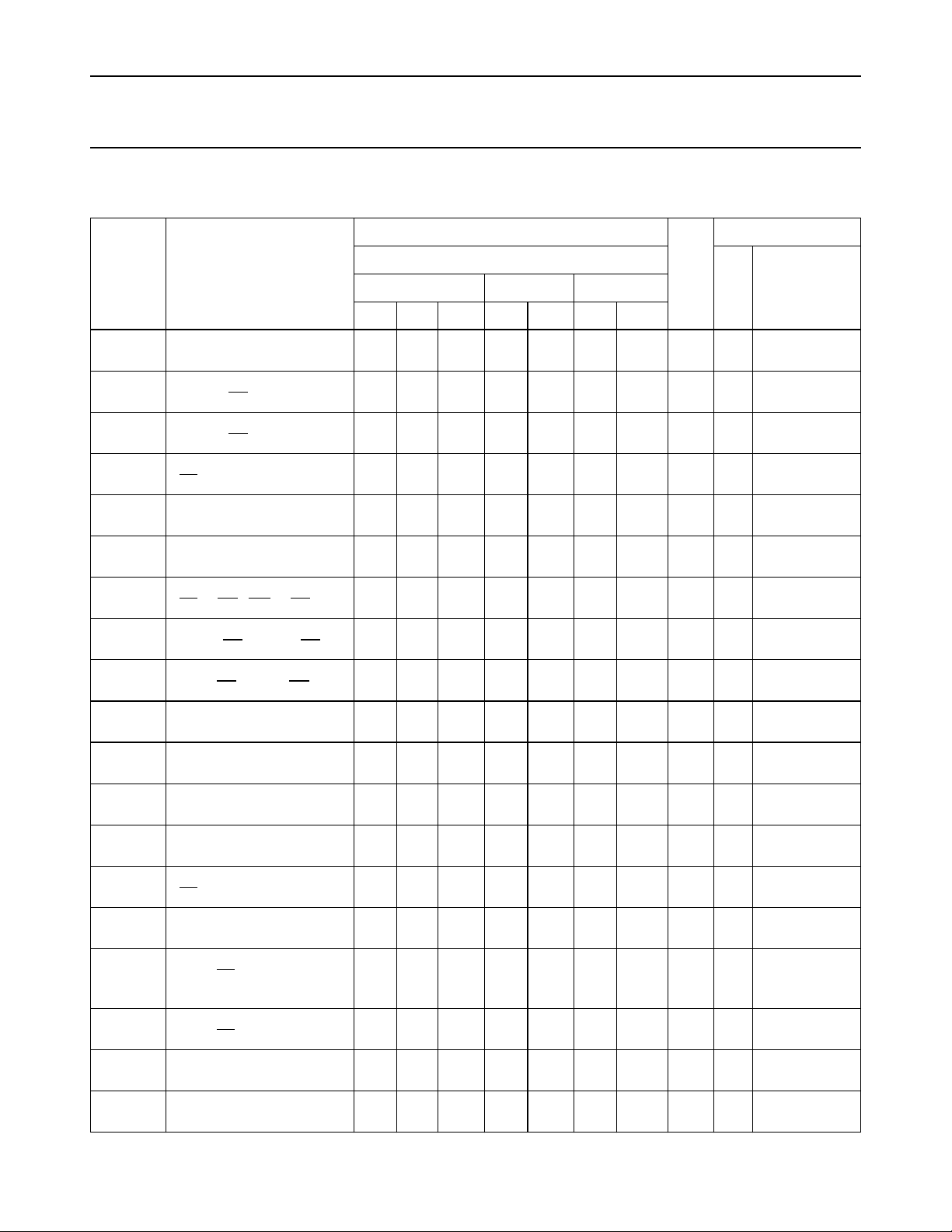
AC CHARACTERISTICS FOR 74HCT
GND = 0 V; t
SYMBOL PARAMETER
/ t
t
PHL
PLH
t
/ t
PHL
PLH
t
/ t
PHL
PLH
/ t
t
PHL
PLH
t
PHL
t
/ t
PHL
PLH
t
/ t
PHL
PLH
t
/ t
PHL
PLH
t
/ t
PHL
PLH
t
/ t
THL
TLH
= 6 ns; CL=50pF
r=tf
+25 −40 to +85 −40 to +125
min. typ. max. min. max. min. max.
propagation delay
CPU, CPD to Q
n
propagation delay
CPU to TC
U
propagation delay
CPD to TC
D
propagation delay
PL to Q
n
propagation delay
MR to Q
n
propagation delay
Dn to Q
n
propagation delay
PL to TCU,PL to TC
propagation delay
MR to TCU,MR to TC
propagation delay
Dn to TCU,Dn to TC
D
D
D
23 43 54 65 ns 4.5 Fig.7
16 30 38 45 ns 4.5 Fig.8
17 30 38 45 ns 4.5 Fig.8
28 46 58 69 ns 4.5 Fig.9
24 40 50 60 ns 4.5 Fig.10
36 62 78 93 ns 4.5 Fig.9
36 64 80 96 ns 4.5 Fig.12
36 64 80 96 ns 4.5 Fig.12
33 58 73 87 ns 4.5 Fig.12
output transition time 7 15 19 22 ns 4.5 Fig.10
T
amb
74HCT
(°C)
74HC/HCT192
TEST CONDITIONS
UNIT
WAVEFORMS
V
CC
(V)
t
W
up, down clock pulse width
25 14 31 38 ns 4.5 Fig.7
HIGH or LOW
t
W
master reset pulse width
16 6 20 24 ns 4.5 Fig.10
HIGH
t
W
parallel load pulse width
20 10 25 30 ns 4.5 Fig.9
LOW
t
t
t
rem
rem
su
removal time
PL to CPU, CP
removal time
MR to CPU, CP
set-up time
10 1 13 15 ns 4.5 Fig.9
D
10 2 13 15 ns 4.5 Fig.10
D
16 8 20 24 ns 4.5 Fig.11 note:
Dn to PL
t
h
hold time
0 −6 0 0 ns 4.5 Fig.11
Dn to PL
t
h
f
max
hold time
CPU to CPD, CPD to CP
maximum up, down clock
20 9 25 30 ns 4.5 Fig.13
U
20 41 16 13 MHz 4.5 Fig.7
pulse frequency
December 1990 10
CPU=CPD=
HIGH
Page 11
Philips Semiconductors Product specification
Presettable synchronous BCD decade
74HC/HCT192
up/down counter
AC WAVEFORMS
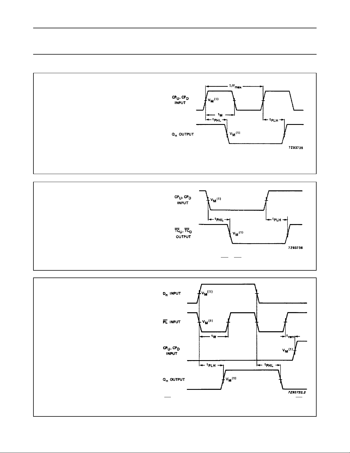
(1) HC : VM= 50%; VI= GND to VCC.
Fig.7 Waveforms showing the clock (CPU, CPD) to output (Qn) propagation delays, the clock pulse width and
= 1.3 V; VI= GND to 3 V.
HCT: V
M
the maximum clock pulse frequency.
(1) HC : VM= 50%; VI= GND to VCC.
= 1.3 V; VI= GND to 3 V.
HCT: V
M
Fig.8 Waveforms showing the clock (CPU, CPD) to terminal count output (TCU, TCD) propagation delays.
(1) HC : VM= 50%; VI= GND to VCC.
= 1.3 V; VI= GND to 3 V.
HCT: V
M
Fig.9 Waveforms showing the parallel load input (PL) and data (Dn) to Qn output propagation delays and PL
removal time to clock input (CPU, CPD).
December 1990 11
Page 12
Philips Semiconductors Product specification
Presettable synchronous BCD decade
74HC/HCT192
up/down counter
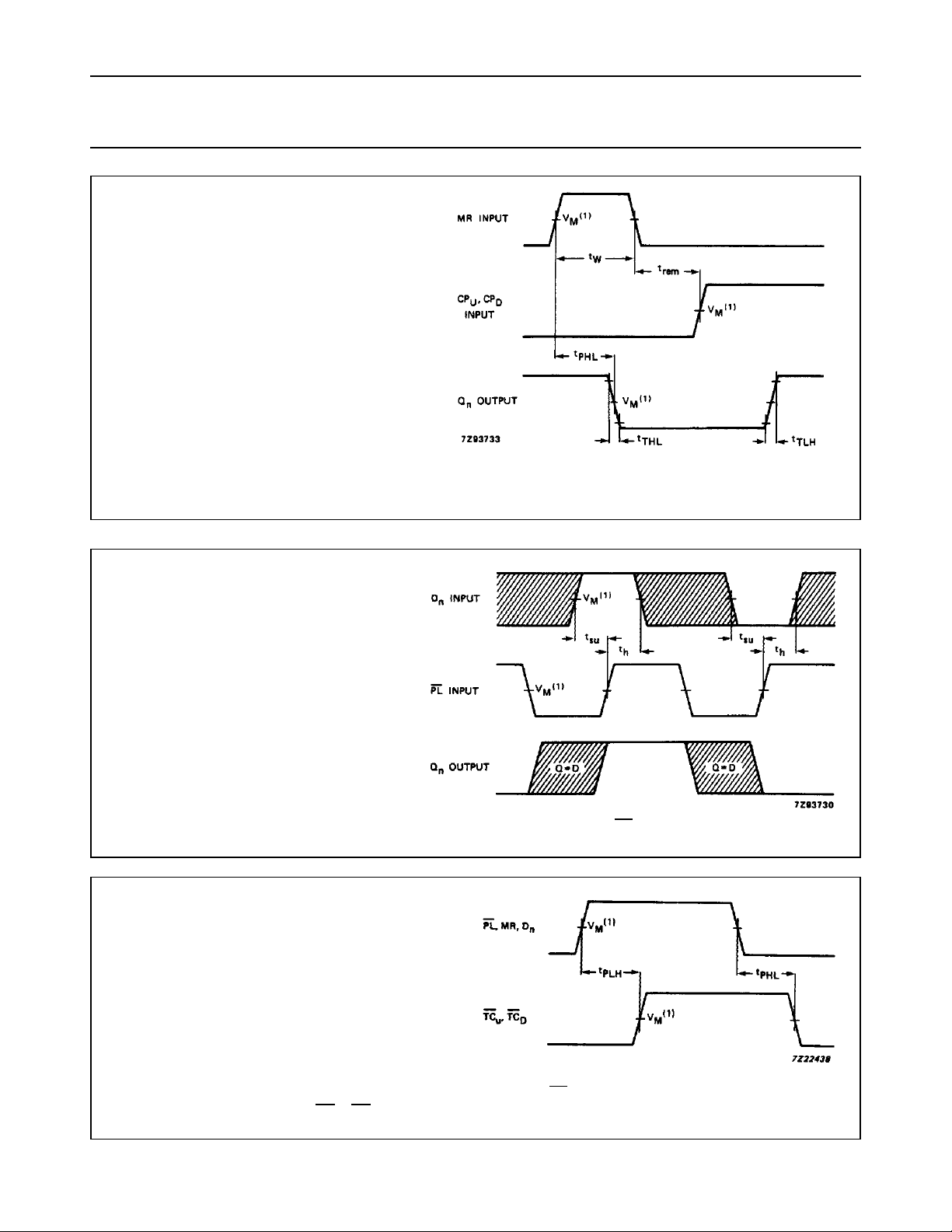
(1) HC : VM= 50%; VI= GND to VCC.
Fig.10 Waveforms showing the master reset input (MR) pulse width, MR to Qn propagation delays, MR to CPU,
= 1.3 V; VI= GND to 3 V.
HCT: V
M
CPD removal time and output transition times.
The shaded areas indicate when the input is permitted
to change for predictable output performance.
(1) HC : V
= 50%; VI= GND to VCC.
M
= 1.3 V; VI= GND to 3 V.
HCT: V
M
Fig.11 Waveforms showing the data input (Dn) to parallel load input (PL) set-up and hold times.
(1) HC : VM= 50%; VI= GND to VCC.
= 1.3 V; VI= GND to 3 V.
HCT: V
M
Fig.12 Waveforms showing the data input (Dn), parallel load input (PL) and the master reset input (MR) to the
terminal count outputs (TCU, TCD) propagation delays.
December 1990 12
Page 13
Philips Semiconductors Product specification
Presettable synchronous BCD decade
up/down counter
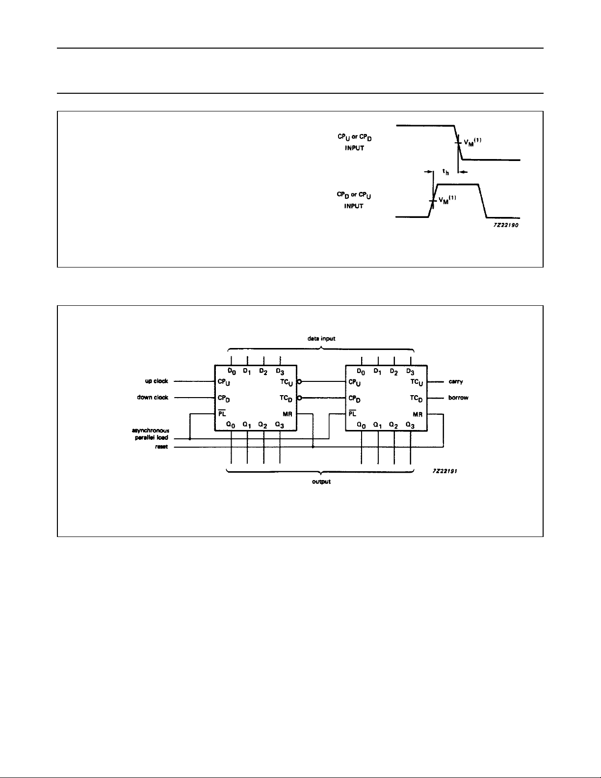
(1) HC : VM= 50%; VI= GND to VCC.
APPLICATION INFORMATION
= 1.3 V; VI= GND to 3 V.
HCT: V
M
Fig.13 Waveforms showing the CPU to CPD or CPD to CPU hold times.
74HC/HCT192
Fig.14 Cascaded up/down counter with parallel load.
PACKAGE OUTLINES
“74HC/HCT/HCU/HCMOS Logic Package Outlines”
See
December 1990 13
.
 Loading...