

Page 1

INTEGRATED CIRCUITS
DATA SH EET
For a complete data sheet, please also download:
•The IC06 74HC/HCT/HCU/HCMOS Logic Family Specifications
•The IC06 74HC/HCT/HCU/HCMOS Logic Package Information
•The IC06 74HC/HCT/HCU/HCMOS Logic Package Outlines
74HC/HCT160
Presettable synchronous BCD
decade counter; asynchronous
reset
Product specification
File under Integrated Circuits, IC06
December 1990
Page 2
Philips Semiconductors Product specification
Presettable synchronous BCD decade
counter; asynchronous reset
FEATURES
• Synchronous counting and loading
• Two count enable inputs for n-bit cascading
• Positive-edge triggered clock
• Asynchronous reset
• Output capability: standard
• ICC category: MSI
GENERAL DESCRIPTION
The 74HC/HCT160 are high-speed Si-gate CMOS devices
and are pin compatible with low power Schottky TTL
(LSTTL). They are specified in compliance with JEDEC
standard no. 7A.
The 74HC/HCT160 are synchronous presettable decade
counters which feature an internal look-ahead carry and
can be used for high-speed counting.
Synchronous operation is provided by having all flip-flops
clocked simultaneously on the positive-going edge of the
clock (CP).
The outputs (Q
HIGH or LOW level. A LOW level at the parallel enable
to Q3) of the counters may be preset to a
0
74HC/HCT160
input (PE) disables the counting action and causes the
data at the data inputs (D0 to D3) to be loaded into the
counter on the positive-going edge of the clock (providing
that the set-up and hold time requirements forPE are met).
Preset takes place regardless of the levels at count enable
inputs (CEP and CET).
A LOW level at the master reset input (MR) sets all four
outputs of the flip-flops (Q0 to Q3) to LOW level regardless
of the levels at CP, PE, CET and CEP inputs (thus
providing an asynchronous clear function).
The look-ahead carry simplifies serial cascading of the
counters. Both count enable inputs (CEP and CET) must
be HIGH to count. The CET input is fed forward to enable
the terminal count output (TC). The TC output thus
enabled will produce a HIGH output pulse of a duration
approximately equal to a HIGH level output of Q0. This
pulse can be used to enable the next cascaded stage.
The maximum clock frequency for the cascaded counters
is determined by the CP to TC propagation delay and CEP
to CP set-up time, according to the following formula:
f
max
---------------------------------------------------------------------------------------------------------
=
t
P max()
CP to TC()+tSU(CEP to CP)
1
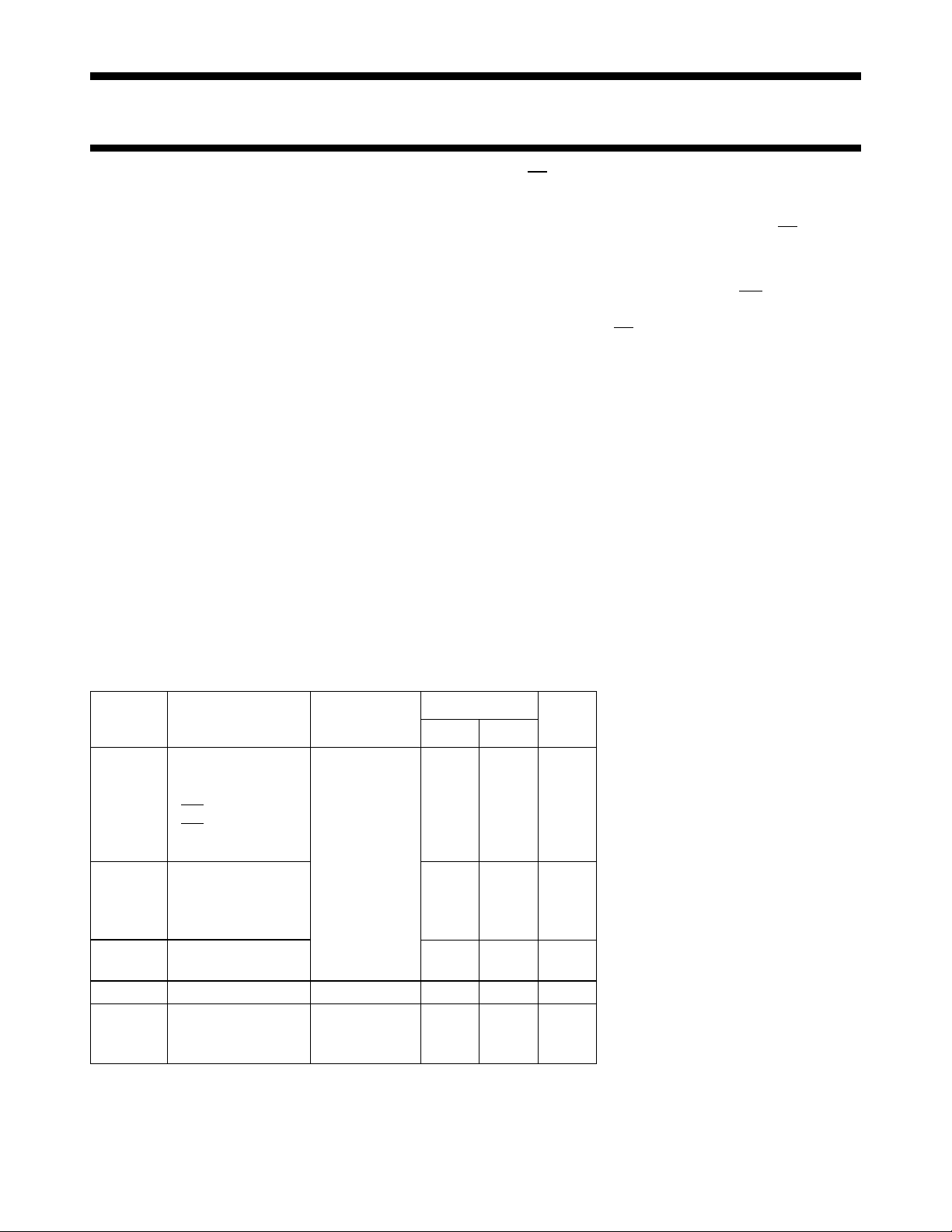
QUICK REFERENCE DATA
GND = 0 V; T
=25°C; tr=tf= 6 ns
amb
SYMBOL PARAMETER CONDITIONS
t
PHL
propagation delay
CP to Q
n
CL=15pF;
VCC=5V 19
CP to TC
MR to Q
n
MR to TC
CET to TC
t
PLH
propagation delay
CP to Q
n
CP to TC
CET to TC
f
max
maximum clock
frequency
C
I
C
PD
input capacitance 3.5 3.5 pF
power dissipation
notes 1 and 2
capacitance per
package
TYPICAL
UNIT
HC HCT
21
21
21
14
19
21
14
21
24
23
26
14
21
20
7
ns
ns
ns
ns
ns
ns
ns
ns
61 31 MHz
39 34 pF
Notes
1. CPD is used to determine the
dynamic power dissipation
(PD in µW):
PD=CPD× V
∑ (CL× V
CC
2
CC
× fi+
2
× fo)
where:
fi= input frequency in MHz
fo= output frequency in MHz
∑ (CL× V
2
× fo) = sum of
CC
outputs
CL= output load capacitance in
pF
VCC= supply voltage in V
2. For HC the condition is
VI= GND to V
CC
For HCT the condition is
VI= GND to VCC− 1.5 V
December 1990 2
Page 3
Philips Semiconductors Product specification
Presettable synchronous BCD decade
counter; asynchronous reset
ORDERING INFORMATION
See
“74HC/HCT/HCU/HCMOS Logic Package Information”
PIN DESCRIPTION
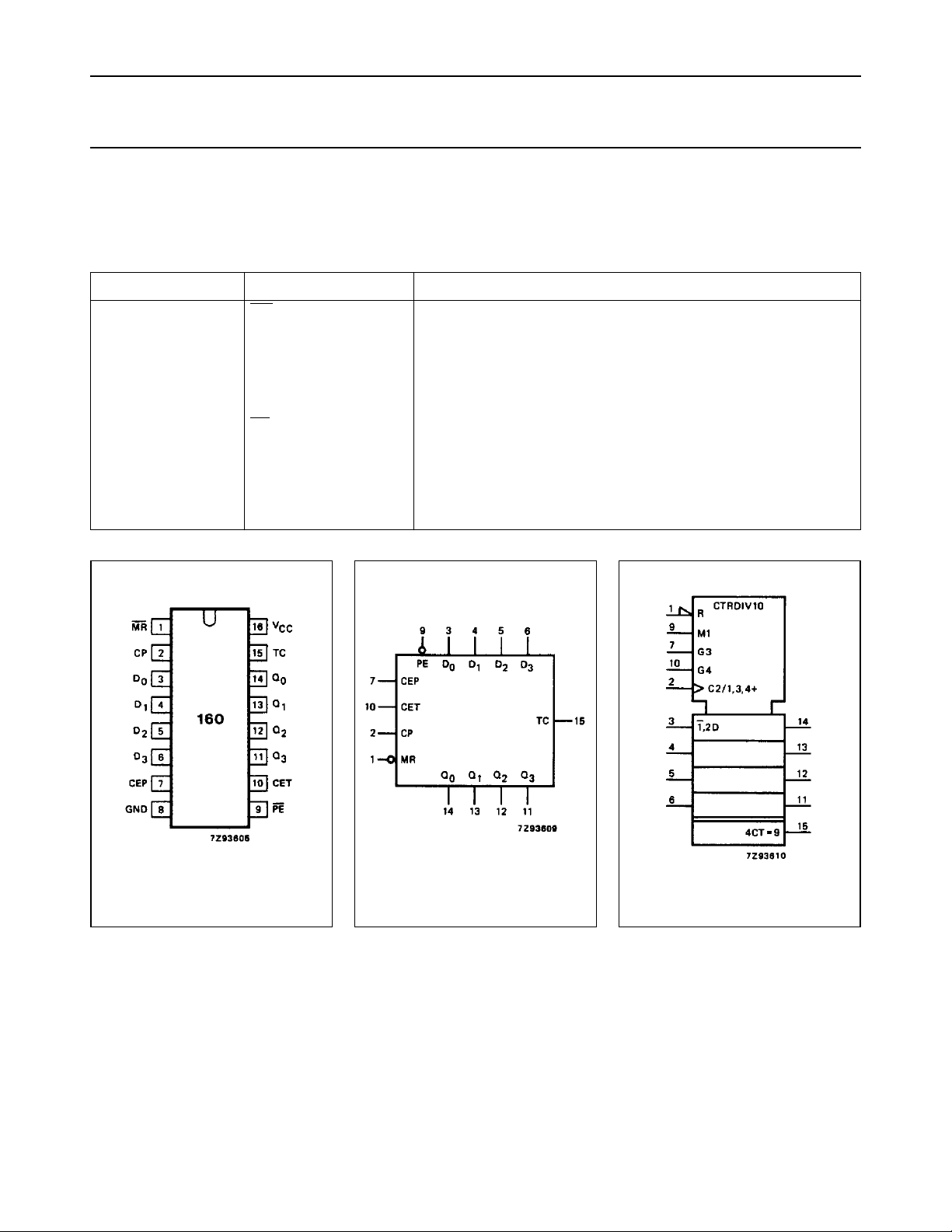
PIN NO. SYMBOL NAME AND FUNCTION
1
2 CP clock input (LOW-to-HIGH, edge-triggered)
3, 4, 5, 6 D
7 CEP count enable input
8 GND ground (0 V)
9
10 CET count enable carry input
14, 13, 12, 11 Q
15 TC terminal count output
16 V
MR asynchronous master reset (active LOW)
to D
0
3
PE parallel enable input (active LOW)
to Q
0
3
CC
data inputs
flip-flop outputs
positive supply voltage
.
74HC/HCT160
Fig.1 Pin configuration. Fig.2 Logic symbol. Fig.3 IEC logic symbol.
December 1990 3
Page 4
Philips Semiconductors Product specification
Presettable synchronous BCD decade
counter; asynchronous reset
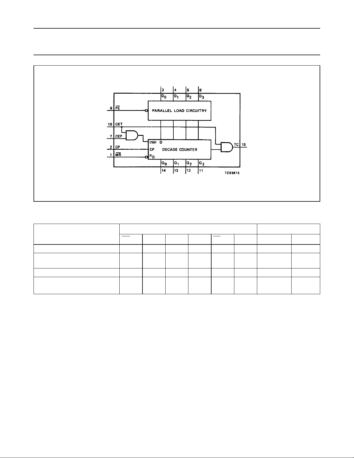
Fig.4 Functional diagram.
74HC/HCT160
FUNCTION TABLE
INPUTS OUTPUTS
OPERATING MODE
MR CP CEP CET PE D
n
Q
n
TC
reset (clear) L XXXXXL L
parallel load H
H
count H ↑ hhhXcount
hold H X I X h X q
(do nothing) H X X I h X q
↑
↑
X
X
X
X
I
I
I
h
L
H
n
n
L
(1)
(1)
(1)
L
Notes
1. The TC output is HIGH when CET is HIGH and the counter is at terminal count (HLLH).
H = HIGH voltage level
h = HIGH voltage level one set-up time prior to the LOW-to-HIGH CP transition
L = LOW voltage level
I = LOW voltage level one set-up time prior to the LOW-to-HIGH CP transition
q = lower case letters indicate the state of the referenced output one set-up time prior to the LOW-to-HIGH CP
transition
X = don’t care
↑ = LOW-to-HIGH CP transition
December 1990 4
Page 5
Philips Semiconductors Product specification
Presettable synchronous BCD decade
counter; asynchronous reset
74HC/HCT160
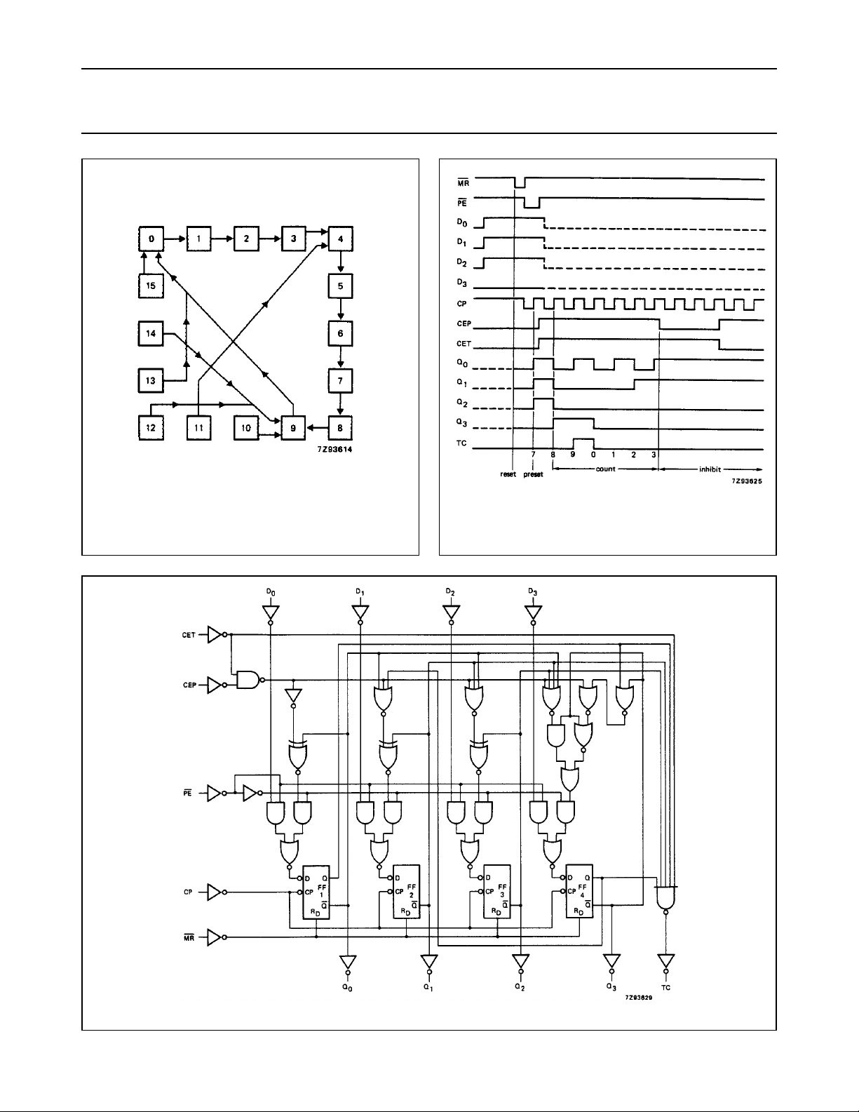
Fig.5 State diagram.
Fig.6 Typical timing sequence: reset outputs to zero;
preset to BCD seven; count to eight, nine, zero,
one, two and three; inhibit.
Fig.7 Logic diagram.
December 1990 5
Page 6
Philips Semiconductors Product specification
Presettable synchronous BCD decade
counter; asynchronous reset
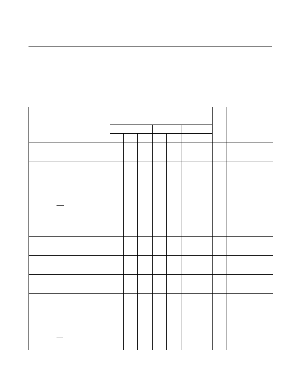
DC CHARACTERISTICS FOR 74HC
For the DC characteristics see
Output capability: standard
ICC category: MSI
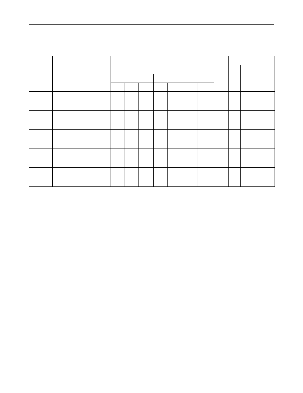
AC CHARACTERISTICS FOR 74HC
GND = 0 V; t
= 6 ns; CL= 50 pF
r=tf
SYMBOL PARAMETER
t
PHL
t
PHL
/ t
/ t
propagation delay
PLH
CP to Q
propagation delay
PLH
n
CP to TC
t
PHL
t
PHL
propagation delay
MR to Q
n
propagation delay
MR to TC
t
PHL
/ t
propagation delay
PLH
CET to TC
t
THL
t
W
/ t
output transition time 19
TLH
clock pulse width
HIGH or LOW
t
W
master reset pulse width
LOW
t
rem
removal time
MR to CP
t
su
set-up time
Dn to CP
t
su
set-up time
PE to CP
“74HC/HCT/HCU/HCMOS Logic Family Specifications”
+25 −40 to +85 −40 to +125
min. typ. max. min. max. min. max.
61
22
18
69
25
20
69
25
20
69
25
20
47
17
14
7
6
80
22
16
8
14
6
80
28
16
10
14
8
100
30
20
11
17
9
80
22
16
8
14
6
135
41
27
15
23
12
185
37
31
215
43
31
210
42
36
220
44
37
150
30
26
75
15
13
T
amb
74HC
100
20
17
100
20
17
125
25
21
100
20
17
170
34
29
(°C)
230
46
39
270
54
46
265
53
45
275
55
47
190
38
33
95
19
16
120
24
20
120
24
20
150
30
26
120
24
20
205
41
35
280
56
48
325
65
55
315
63
54
330
66
56
225
45
38
110
22
19
.
74HC/HCT160
TEST CONDITIONS
UNIT
ns 2.0
ns 2.0
ns 2.0
ns 2.0
ns 2.0
ns 2.0
ns 2.0
ns 2.0
ns 2.0
ns 2.0
ns 2.0
WAVEFORMS
V
CC
(V)
Fig. 8
4.5
6.0
Fig. 8
4.5
6.0
Fig. 9
4.5
6.0
Fig. 9
4.5
6.0
Fig. 10
4.5
6.0
Figs 8 and 10
4.5
6.0
Fig. 8
4.5
6.0
Fig. 9
4.5
6.0
Fig. 9
4.5
6.0
Fig. 11
4.5
6.0
Fig. 11
4.5
6.0
December 1990 6
Page 7
Philips Semiconductors Product specification
Presettable synchronous BCD decade
counter; asynchronous reset
SYMBOL PARAMETER
t
su
set-up time
CEP, CET to CP
t
h
hold time
Dn to CP
t
h
hold time
PE to CP
t
h
hold time
CEP, CET to CP
f
max
maximum clock pulse
frequency
min. typ. max. min. max. min. max.
200
40
34
0
0
0
0
0
0
0
0
0
6.0
30
35
+25 −40 to +85 −40 to +125
63
23
18
−17
−6
−5
−41
−15
−12
−58
−21
−17
18
55
66
T
amb
74HC
250
50
43
0
0
0
0
0
0
0
0
0
4.8
24
28
(°C)
300
60
51
0
0
0
0
0
0
0
0
0
4.0
20
24
74HC/HCT160
TEST CONDITIONS
UNIT
ns 2.0
ns 2.0
ns 2.0
ns 2.0
MHz 2.0
WAVEFORMS
V
CC
(V)
Fig. 12
4.5
6.0
Figs 11 and 12
4.5
6.0
Figs 11 and 12
4.5
6.0
Figs 11 and 12
4.5
6.0
Fig. 8
4.5
6.0
December 1990 7
Page 8

Philips Semiconductors Product specification
Presettable synchronous BCD decade
74HC/HCT160
counter; asynchronous reset
DC CHARACTERISTICS FOR 74HCT
For the DC characteristics see
Output capability: standard
ICC category: MSI
Note to HCT types
The value of additional quiescent supply current (∆I
To determine ∆ICC per input, multiply this value by the unit load coefficient shown in the table below.
INPUT UNIT LOAD COEFFICIENT
MR 0.95
CP 0.80
CEP 0.25
D
n
CET 1.05
PT 0.30
0.25
“74HC/HCT/HCU/HCMOS Logic Family Specifications”
) for unit load of 1 is given in the family specifications.
CC
.
December 1990 8
Page 9
Philips Semiconductors Product specification
Presettable synchronous BCD decade
counter; asynchronous reset
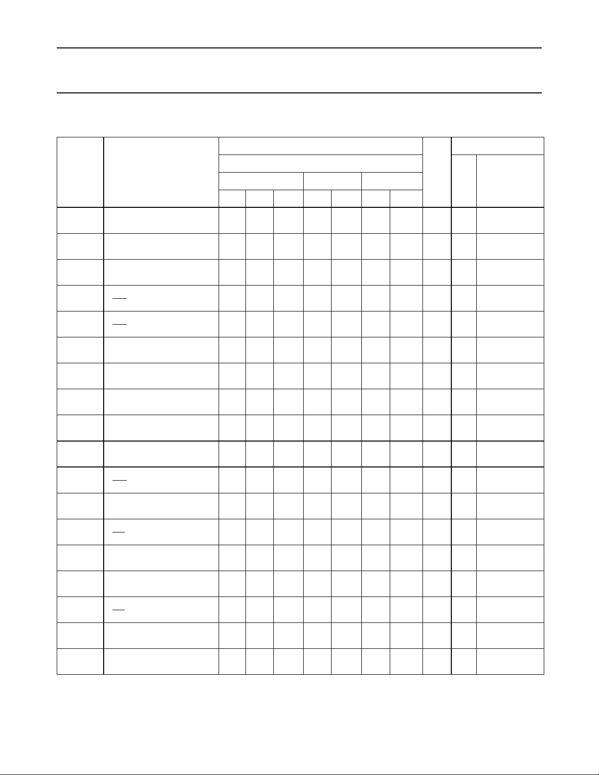
AC CHARACTERISTICS FOR 74HCT
GND = 0 V; t
SYMBOL PARAMETER
/ t
t
PHL
PLH
t
PHL
t
PLH
t
PHL
t
PHL
t
PHL
t
PLH
t
/ t
THL
TLH
= 6 ns; CL= 50 pF
r=tf
+25 −40 to +85 −40 to +125
min. typ. max. min. max. min. max.
propagation delay
CP to Q
n
propagation delay
25 43 54 65 ns 4.5 Fig. 8
28 48 60 72 ns 4.5 Fig. 8
CP to TC
propagation delay
23 39 49 59 ns 4.5 Fig. 8
CP to TC
propagation delay
MR to Q
n
propagation delay
27 50 63 75 ns 4.5 Fig. 9
30 50 63 75 ns 4.5 Fig. 9
MR to TC
propagation delay
17 35 44 53 ns 4.5 Fig. 10
CET to TC
propagation delay
9 17 21 26 ns 4.5 Fig. 10
CET to TC
output transition time 7 15 19 22 ns 4.5 Figs 8 and 10
T
amb
74HCT
(°C)
74HC/HCT160
TEST CONDITIONS
UNIT
WAVEFORMS
V
CC
(V)
t
W
clock pulse width
HIGH or LOW
t
W
master reset pulse width
LOW
t
rem
removal time
MR to CP
t
su
set-up time
Dn to CP
t
su
set-up time
PE to CP
t
su
set-up time
CEP, CET to CP
t
h
hold time
Dn to CP
t
h
hold time
PE to CP
t
h
hold time
CEP, CET to CP
f
max
maximum clock pulse
frequency
PACKAGE OUTLINES
16 8 20 24 ns 4.5 Fig. 8
20 11 25 30 ns 4.5 Fig. 9
20 9 25 30 ns 4.5 Fig. 9
18 10 25 30 ns 4.5 Fig. 11
30 18 44 53 ns 4.5 Fig. 11
50 30 63 75 ns 4.5 Fig. 12
0 −8 0 0 ns 4.5 Figs 11 and 12
0 −13 0 0 ns 4.5 Figs 11 and 12
0 −21 0 0 ns 4.5 Figs 11 and 12
16 28 13 11 MHz 4.5 Fig. 8
See
“74HC/HCT/HCU/HCMOS Logic Package Outlines”
.
December 1990 9
 Loading...